1. Introduction
The recent diffusion of wideband communication systems and high-frequency measurement systems drives the development of analog-to-digital (ADC) [
1] and digital-to-analog (DAC) converters [
2] operating with sampling frequencies of tens of GHz. Such converters usually require low-pass filters (LPFs) with bandwidth ranging from DC to GHz frequencies to be used as anti-aliasing filters in ADCs and shaping filters in DACs. To allow processing very wide signal bandwidths, digitizer architectures based on the multiply-filter-processing (MFP) paradigm have been proposed [
3], and they also require LPFs with GHz bandwidths. All these applications usually require high-order filters to achieve a large out-of-band suppression, and they can be implemented by cascading biquad stages with suitable resonance frequencies and quality factors. Technology limitations pose constraints on the maximum quality factor that can be achieved, and this can be coped with by a suitable system design of the overall filter. Noise and distortions, which determine the dynamic range of the filter, are the main design specifications; the high level of integration of the systems adds further requirements on the minimization of power consumption and area footprint.
Active filters are usually designed according to the gyrator synthesis method starting from an LC-ladder prototype [
4], to the leapfrog LC-ladder simulation technique [
5], or as a cascade of biquadratic sections (biquad) [
6]. In the GHz frequency range, the traditional approach to designing filters involves the use of real inductors in such active structures or in passive networks [
7,
8]. The use of inductors, however, is in contrast with the requirements of high integration, since on-chip inductors require a huge amount of area and are prone to electromagnetic interferences. Moreover, the constraints on practically realizable inductance values could lead to high power consumption, and the low quality factor and the large parasitic effects could limit the design space to achieve the desired frequency response.
The design of multi-GHz filters that do not use physical inductors is therefore an active field of research, and several low-pass and bandpass filters have been proposed in the literature. The most common approaches are the Gm-C architecture in the few-GHz range [
4,
5,
9] and the use of RLC reference structures with active inductors [
6,
10,
11] for frequencies around 10 GHz. Low-frequency approaches such as the Sallen-Key [
12,
13,
14] and Tow-Thomas biquads [
15] have also been reported, and the availability of deep sub-micron CMOS and SiGe BiCMOS technologies with f
T of hundreds of GHz [
16,
17] has allowed applying the Sallen-Key architecture up to 17 GHz [
18].
While BiCMOS technologies surely allow very high frequencies using such low-frequency approaches, the trend towards the use of CMOS technologies for ever higher frequencies leads to exploring the design of inductor-less biquads operating at 10 GHz in CMOS. In this context, open-loop architectures, such as Gm-C and the use of active inductors, seem preferable to closed-loop ones to achieve high frequencies. For low-frequency applications, open-loop active-C biquad structures based on the flipped voltage follower (FVF) and super source follower (SSF) topologies have been proposed, and they appear to be a good candidate to achieve CMOS biquads with GHz-range frequencies and low power consumption [
19,
20]. A 7.5 GHz biquad based on the FVF-C approach was proposed in [
21] using a 28 nm CMOS technology. It extends to high frequencies the approach used in [
20], but the availability of a single control terminal makes it impossible to separate the control of the resonance pulsation ω
0 and of the quality factor Q. Tuning of ω
0 and Q would instead be useful both to compensate for process variations and to allow the tunability of the filter to adapt it to different applications.
In this paper, we propose a biquad architecture based on the use of the SSF that allows achieving a 3 dB bandwidth of 8 GHz in a 28 nm FDSOI CMOS technology with a power consumption below 1 mW. The architecture can be implemented in two complementary forms (NMOS input and PMOS input), thus allowing easy cascadability, overcoming the different input and output voltage levels in the SSF topology. The SSF topology allows separate (and ideally orthogonal) tuning of ω
0 and Q of the biquad, thus improving with respect to the filter in [
21]. The biquads have been designed to maximize bandwidth and minimize power consumption; this somehow limits the dynamic range; however, a comparison with the state of the art shows interesting performance, also taking into account the possibility of trading power for dynamic range.
This paper is organized as follows.
Section 2 introduces the proposed topology, discussing its nonideal effects that cannot be neglected at high frequency.
Section 3 summarizes the simulation results and provides a comparison with the literature, and
Section 4 concludes this study.
2. Analysis of the Topology
This section analyzes the proposed biquad topology in terms of frequency response, impact of parasitic effects, and large-signal performance.
2.1. Analysis of the SSF-Based Biquad
Inductor-less biquads usually are based either on closed-loop architectures (Sallen-Key, Tow-Thomas) [
12,
13,
14] or on open-loop structures such as Gm-C, active-C, or RLC equivalents exploiting active inductors [
6,
9]. With the goal of maximizing the resonance frequency for a given power level, open-loop architectures have a net advantage, and in particular, the simpler topology creates fewer extra poles and zeros that affect the high-frequency behavior of the biquad, limiting the maximum cutoff frequency.
As a consequence, the source-follower-C (SF-C) filter class is a good candidate to design biquads with very high cutoff frequency and good overall performance, since they use a limited number of devices and hence of internal nodes that add extra poles that are desired to be out of band. In particular, biquads based on the flipped voltage follower (FVF) and on the super source follower (SSF) topologies have been proposed in the literature, aimed at low-frequency biomedical applications [
19,
20].
Figure 1 shows the topology of FVF and SSF stages as follows: by an analysis of the schematics, it is clear that their small-signal behavior is identical, since the SSF can be interpreted as the folded version of the FVF. They both form a unitary-gain loop with the same input and output impedances and voltage and current gains. However, the folded nature of the SSF yields more flexibility in accommodating voltage swings at the internal high impedance node; thus, we select it to design a multi-GHz low-pass biquad. The structure can be considered a current-mode circuit as follows: M
1 is an inverting second-generation current conveyor (CCII), whereas M
2 is a transconductance. The combination of the two yields a CFOA (current-feedback operational amplifier) without the output low-impedance stage.
It has to be noted that source follower structures provide a DC level shift between input and output equal to a gate-source voltage. While this is not an issue for a single biquad, it can impair the cascading of stages to achieve higher-order filters with a limited supply voltage range. However, the complementary nature of CMOS technology allows overcoming this issue by alternating stages based on NMOS and PMOS input devices (N-type and P-type biquads in the following), as shown in
Figure 2.
2.2. Ideal Frequency Response
The proposed biquad, shown in
Figure 2 in the N-type and P-type configurations, is composed of a super source follower with two additional capacitors, one between the output node and the internal high-impedance node, and the other between the output node and ground. In practice, transistor M
1 acts as a current conveyor with the gate as the Y terminal, the source as the X terminal, and the drain as the Z terminal; the high-impedance load at the Z terminal and the common-source amplifier (M
2) close the feedback loop. The current generator I
B1 sets the bias current of M
1, whereas current generator I
B2 draws the sum of the currents of M
1 and M
2: having two current sources allows easier tuning of biquad parameters than in the FVF case [
21], as we will show in the following text.
Figure 3 shows the small-signal equivalent circuit of the proposed topology: transistors M
1 and M
2 are modeled by their transconductance
, their output conductance
, where
is the intrinsic gain of the device, and their gate-source capacitance is
(we are neglecting the capacitance between gate and drain). Moreover, body transconductance
is considered for transistor M
1 (we assume the body terminal is connected to a fixed voltage). Current sources are modeled by their output conductances
. Gate-drain capacitances are neglected.
Neglecting the capacitances
and the output conductances
,
of the transistors, the ideal transfer function can be easily calculated as follows:
where
Because and are functions of the biasing currents of the corresponding transistors, it is possible to tune the frequency response to compensate for the variations in both and . Scaling the two currents by the same amount leaves the ratio roughly unchanged and ideally affects only . On the other hand, changing the two currents in opposite directions has a larger impact on and ideally no impact on . The control could therefore independently set the ratio and product of the ’s to set the two parameters separately, because they will impact the two parameters differently. Because the filter is in unity feedback configuration, the low-frequency gain is always close to 0 dB at DC and cannot be tuned.
In the following subsections, we will analyze the impact of parasitic elements of the transistors on the transfer function (1).
2.3. Effect of Parasitic Capacitances
The two main parasitic capacitances in
Figure 3 are the
of the two transistors, M
1 and M
2. We assume for simplicity that
for both transistors, with
,
. The frequency response of the biquad, including these capacitances, can be calculated from the circuit in
Figure 3, neglecting the conductances
, as follows:
The impact on the poles is limited if
, but two negative zeros appear. Unfortunately, the second-order term at the numerator is large with respect to the first-order term, so that the zeros will be complex conjugated with a large quality factor:
Because the number of zeros is equal to the number of poles, the gain at infinity is finite as follows:
However, the asymptotic gain is low if
. It has to be noted that the zeros set a limit to the maximum bandwidth that can be achieved for a given level of out-of-band attenuation.
As for the poles of the biquad, the expressions for the resonance frequency and the quality factor are reported below:
Equations show that the resonance frequency is slightly reduced by the additional capacitances, whereas the impact on the quality factor can be positive or negative.
2.4. Effect of Parasitic Resistances
There are two nodes in the circuit where the parasitic resistances of the current generators and of M1 and M2 are present. M1 adds a parasitic resistance in parallel with , the other devices, which add parasitic resistances from one of the two nodes (output and high-impedance internal node) toward ground.
To make this analysis more meaningful, we assume that all output conductances are proportional to the respective transconductances as follows:
where
(the intrinsic gain of the transistor) in the case of simple transistors (i.e.,
) and
in the case of cascodes. Moreover, we assume
and
, i.e., the output conductances of the current sources are proportional to their currents, and devices implementing them are sized with the same overdrive voltage as M
1 and M
2.
With these assumptions, the frequency response is as follows:
Equation (12) shows that parasitic resistances reduce the DC gain, slightly increase the resonance frequency, and reduce the quality factor. No additional poles or zeros are created.
The most interesting effect of the parasitic resistances is that they result in a maximum quality factor that can be achieved by using this biquad topology. Defining the capacitive ratio
and the resistive ratio
, the quality factor can be calculated as follows:
Equation (13) shows that the quality factor cannot go to infinity, and to achieve
, it is necessary to have
. This cannot be obtained in advanced CMOS processes using simple minimum-length devices, so the devices must be cascoded to obtain a higher gain
, hence a higher resistance.
2.5. Impact of Cascoding
The output resistances can be removed (improved by a factor
) by cascoding, and each transistor in the actual circuit (including the current generators) is in fact cascoded. However, cascoding adds a pole to the transconductances at the frequency of the cascoding device, i.e.,
, and these poles modify the frequency response of the filter, adding two poles at high frequency. The resulting transfer function is as follows:
With a fourth-order polynomial, it is hard to find an interesting expression for the poles; assuming the first two poles to be dominant with respect to the parasitic poles, however, provides a simple separation:
The first two terms will be affected by the terms in
, but the effect is limited as long as
. However, both
and Q tend to increase with the additional poles, which will be at a much higher frequency. All these effects are usually negligible but can become significant when this topology is exploited to design very high-frequency biquads.
2.6. Noise Analysis
Noise of the biquad is analyzed in the ideal case, neglecting the effect of parasitic resistors and capacitors. The schematic in
Figure 4 shows the corresponding small-signal circuit, including noise sources. I
n1 and I
n2 are the noise sources related to devices M
1 and M
2 and, in the schematic, are in parallel to the controlled sources g
miV
gsi (i = 1, 2), whereas I
nB1 and I
nB2 are the noise sources associated with the current generators. It has to be noted that noise sources I
n2 and I
nB2 result in parallel between the output node and ground. Each noise source has a power spectral density.
where K
B is the Boltzmann constant; T is the absolute temperature; C
ox is the oxide capacitance per unit area; W and L are the channel width and length, respectively; and γ and K
F are process-dependent coefficients. The flicker component is neglected in the following due to the wide filter bandwidth.
Analysis of the schematic in
Figure 4 provides the output voltage due to the noise sources in the following form:
that shows that the different noise sources go through different frequency behavior. Considering the corresponding power spectral density and substituting Equations (3) and (4), the output noise power spectral density can be expressed, highlighting low-pass and bandpass components:
and integrating over frequency, the total equivalent output noise power is obtained:
2.7. Cascadability of Biquads
The cascading of an N-type and of a P-type biquad, shown in
Figure 5, allows input and output biasing voltages of the overall 4th-order filter to be the same but constrains the output voltage at the intermediate node. For simplicity, we assume
for all NMOS and PMOS devices the same threshold voltage
(and hence overdrive voltage
). According to the previous discussion, all devices have been cascoded.
The condition to have M
B2N, M
1N, M
1P, and M
B2P (and the respective cascoding devices) all operating in the saturation region is as follows:
whereas M
2N and M
2P’s constraints are not binding because other devices enter the triode regions before. We have assumed that the cascoded devices are biased at the minimum required
voltage. From the above equations, the minimum supply voltage to have proper biasing is as follows:
3. Simulation Results
The N-type and P-type biquads in
Figure 5 have been designed and simulated in the 28 nm CMOS FDSOI (fully-depleted Silicon-on-Insulator) technology by STMicroelectronics [
17]. Both biquads have been designed to achieve a resonance frequency of 5.8 GHz and a quality factor Q = 2.
Table 1 reports the sizing of all devices that have been designed with minimum gate length to maximize the transition frequency. Supply voltage is 1.2 V. Forward body bias has been exploited to reduce the threshold voltage and further increase device speed. The use of an FDSOI process allows setting the voltage on the body terminal without the risk of the body-channel junction turning on; thus, voltages outside the supply rails have been exploited to bias the body terminals of M
1 and M
2 (including cascode devices). Chosen values are 1 V and −0.6 V for NMOS and PMOS devices. Reported values of the capacitors refer to the explicit capacitors that have been implemented; device and layout parasitics add to these values, and the effect is particularly significant for
C2. The design goal was to maximize the bandwidth with minimum area and power consumption; this requires using small capacitors, whose minimum value is determined by technological constraints and the effect of layout parasitics.
Figure 6 shows the layout of the N-type and P-type biquads, whose size is 15.5 × 25 μm
2. The filters thus result in a very compact design, minimizing parasitic effects of layout and routing lines.
3.1. Performance in Nominal Conditions
Post-layout simulations in nominal conditions (typical process corner, 27 °C, 1.2 V supply voltage) have been performed to assess the performance of the designed biquads. Power dissipation is 820 μW and 670 μW for the N-type and P-type biquads, respectively.
Figure 7 shows the frequency response of the N-type, P-type, and cascaded (N + P) filters. Resonance frequency and quality factor are 5.4 GHz (5.5 GHz) and 6.6 dB (7.2 dB) for the N-type (P-type) biquad, and the cutoff frequency is about 8 GHz for both biquads. Out-of-band gain saturates to −30 dB because of the complex zeros in (4); obviously, out-of-band gain drops to −60 dB for the cascade of the two biquads, making the suppression of out-of-band components not an issue in practical cases.
Simulations have been performed to verify the tunability of filter parameters through the bias currents I
B1 and I
B2. As discussed in
Section 2, the resonance frequency and the quality factor can be adjusted separately by a suitable control of the bias currents.
Figure 8 and
Figure 9 show the case of tuning of the resonance frequency with an (ideally) constant quality factor, achieved by keeping the ratio of
and
constant, so that I
B2 scales by the same factor K as I
B1. Second-order effects result in some variation in the quality factor, and the resonance frequency shows about a 50% tuning range. More specifically, for typical process parameters (corner TYP), the resonance frequency goes from 3.5 GHz to 5.9 GHz (3.3 GHz to 5.7 GHz) for K varying between 0.45 and 1.3 (0.3 and 1.1) for the N-type (P-type) biquad, with about 1 dB variation in the quality factor.
Figure 10 and
Figure 11 show the case of changing the quality factor while keeping the resonance frequency constant. In this case, the ratio of
and
needs to be varied while keeping their product constant; hence, the currents of M
1 and M
2 have to be varied in opposite directions. Currents are defined as follows:
hence
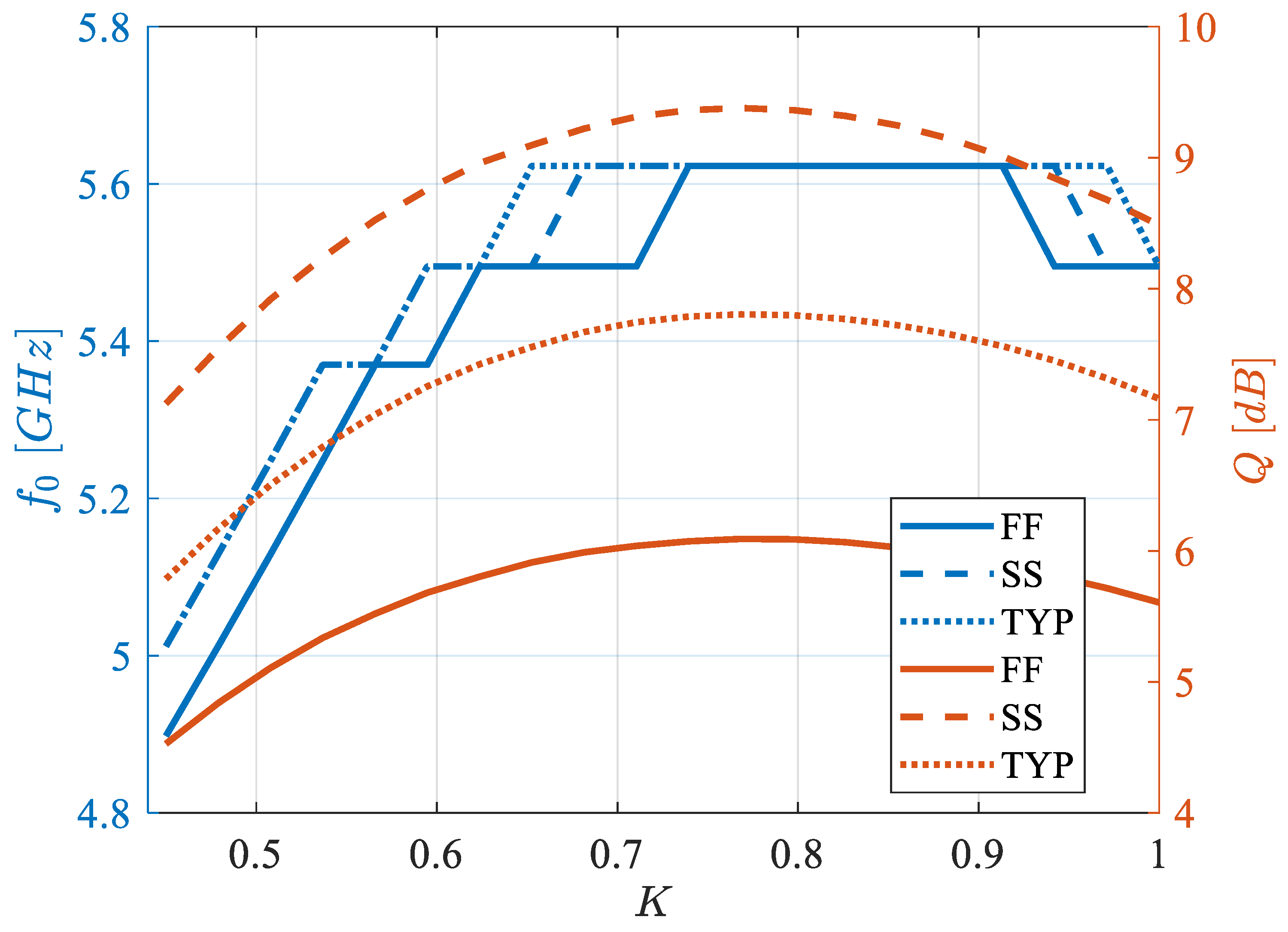
Simulations show a good range of tunability for the quality factor (about 3 dB) with a limited variation in the resonance frequency. For typical process parameters (corner TYP), the quality factor changes from 3.5 dB to 7 dB for N-type biquad with K ranging from 0.4 to 1, and from about 5.6 dB to 7.8 dB for P-type biquad; the corresponding variation in resonance frequency is about 1 GHz for the N-type biquad (4.2 GHz to 5.2 GHz) and 600 MHz (5 GHz to 5.6 GHz) for the P-type one. Controls on resonance frequency and quality factor result in non-orthogonality due to the effect of secondary poles and zeros that are not negligible at such high frequencies, but anyway, the resulting control ranges allow us to counteract the effect of process variations, as will be shown in the next subsection.
Figure 8,
Figure 9,
Figure 10 and
Figure 11 also report the tuning curves for the best and worst process corners (corners FF = fast fast and SS = slow slow), showing that variation in resonance frequency with process can be easily recovered by varying the tuning current. The situation is more critical for what concerns Q, since the filter was designed around the maximum Q that can be achieved in nominal conditions.
Figure 12 shows the output noise spectrum for both biquads, resulting in a noise corner frequency of about 2 MHz and an in-band integrated output noise of 1.44 mVrms for the N-type biquad and 1.5 mVrms for the P-type biquad.
Figure 13 reports the DC transcharacteristic, which shows the input–output level shift and a linear range of about 400 mVpp. This is further confirmed by
Figure 14, which shows the output spectrum for a two-tone test with 200 mVpp sinusoidal signals at 900 MHz and 1 GHz. Third-order intermodulation distortion (IMD3) is −49.7 dB and −52.9 dB for the N-type and P-type biquads, respectively. The spectrum also shows a second-harmonic distortion (HD2) of about −33.13 dB (−33.44 dB), due to the single-ended nature of the biquad, and a third-harmonic distortion (HD3) of −44 dB (−46.8 dB) for the N-type (P-type) biquad.
3.2. Robustness to PVT Variations and Mismatches
To assess the robustness of the biquads to supply voltage and temperature variations, simulations have been carried out considering ±10% supply voltage variations and 0 °C and 80 °C temperatures.
Table 2 and
Table 3 synthesize the results for N-type and P-type biquads, together with the nominal performance.
It is interesting to note that variation in the resonance frequency is less than the range that can be covered by a variation in bias currents, shown in
Figure 8 and
Figure 9, thus allowing the effect to be compensated.
Joint process and mismatch Monte Carlo simulations have been carried out to verify the effect of process variations (both of MOS transistors and capacitors) and mismatches.
Table 4 reports the results after 200 Monte Carlo iterations, showing a good robustness of both resonance frequency
and quality factor Q, with standard-deviation-to-mean ratios below 3.5% (for
) and 7.5% (for Q).
3.3. Comparison with the Literature
In this subsection, we compare the performance of the proposed biquads with other multi-GHz inductor-less low-pass filter implementations from the literature. Figures of merit (FOMs) are typically used to allow a fair comparison and highlight the trade-offs in the designs. In particular, the following figures of merit commonly used in the filter literature have been exploited:
Figure of merit FOM
1 simply normalizes the power dissipation
to the number of poles
to allow a comparison between filters of different order. Figure of merit FOM
2 also takes into account the 3 dB bandwidth of the filter
, highlighting the trade-off between power and frequency. Figure of merit FOM
3 also includes the dynamic range
, expressed in a linear scale:
(
in (29) is the dynamic range in decibels.). The dynamic range
is defined as the difference (in dB) between the signal level that corresponds to maximum signal-to-noise-and-distortion ratio (SNDR) and the noise level (i.e., SNR = 0).
Table 5 shows a comparison with the literature. Some reported that filters are implemented using BiCMOS; others use CMOS. CMOS implementations are expected to require lower power, but bandwidth and dynamic range can be limited, so the latter two FOMs may be challenging.
The proposed biquads have the lowest consumption in the literature, and the only CMOS implementation with a larger bandwidth has more than 150 times the power dissipation. The very low power consumption increases the SNR and thus limits the dynamic range of the filter. Hence, while the proposed biquads have remarkable FOM
1 and FOM
2 performance (consumption per pole and consumption per pole and bandwidth), the FOM
3 (which also includes the dynamic range) is good, but some other implementations are more efficient because of higher linearity and lower noise. The biquads were designed to minimize power consumption, and the resulting dynamic range (about 34 dB) could be limited for some applications. However, it is comparable with other studies in the literature ([
21,
22]) and could be increased at the expense of increased power consumption. The proposed biquads also have the lowest area occupation in the literature, almost one order of magnitude lower than comparable filters.
Table 5.
Comparison with the literature.
Table 5.
Comparison with the literature.
| Performance | This Study | [21] | [18] | [23] | [6] | [22] | [13] | [5] | [4] |
|---|
| N-Type | P-Type | N-Type | P-Type |
|---|
| Tech. (nm) | CMOS 28 FDSOI | CMOS 28 FDSOI | BICMOS | CMOS 22 | BICMOS | CMOS 90 | BICMOS | CMOS 28 | CMOS 22 |
| Npole | 2 | 2 | 2 | 2 | 2 | 5 | 6 | 4 | 2 | 5 | 3 |
| VDD (V) | 1.2 | 1.2 | 1.2 | 1.2 | 2.7 | 0.8 | 3 | 1 | 3 | 1.1 | 1.4 |
| Pdiss (mW) | 0.82 | 0.67 | 1.08 | 1.6 | 15.75 | 19.9 | 43 | 3.7 | 18 | 30 | 140 |
| f3dB (GHz) | 8.1 | 7.9 | 7.57 | 7.2 | 17.1 | 4.9 | 10.3 | 1 | 9.55 | 3.3 | 10 |
| A0 (dB) | −1.9 | −2.3 | −1.6 | −1.8 | 3.8 | 0.5 | −0.2 | 0 | −0.5 | −1 | 1.3 |
| Pinoise (dBm) | −44.7 | −45.4 | −43.5 | −39.4 | −50.4 | −56.8 | −45.9 | −46 | −46.8 | −56 | −55.6 |
| (dBm) | −10 | −10 | −10 | −10 | −2.9 | | −1 | −13 | −1 | −17 | −10.6 |
| THD (dB) @ | −33.1 | −33.4 | −46.8 | −42.4 | −51.7 | | −42.6 | −41.77 | −64 | −40 | −45 |
| IIP3 (dBm) | | | | | 17.25 | 5.5 | | | | | |
| DR (dB) | 33.9 | 34.4 | 40.2 | 35.9 | 47.9 | 41.7 | 43.1 | 34.9 | 50.9 | 38.4 | 44 |
| Area (mm2) | 0.00038 | 0.00038 | 0.000246 | 0.000193 | 0.0025 | 0.05 | 0.02 | 0.000092 | 0.0027 | 0.09 | 0.01 |
| Area/pole (mm2) | 0.00019 | 0.00019 | 0.000123 | 0.000096 | 0.00125 | 0.01 | 0.003 | 0.000023 | 0.00135 | 0.018 | 0.003 |
| FOM1 (mW) | 0.41 | 0.33 | 0.54 | 0.3 | 7.87 | 3.98 | 7.2 | 0.925 | 9 | 6 | 46.7 |
| FOM2 (pW/Hz) | 0.051 | 0.042 | 0.071 | 0.042 | 0.461 | 0.812 | 0.696 | 0.925 | 0.942 | 1.818 | 4.667 |
| FOM3 (aW/Hz) | 20.52 | 15.31 | 6.82 | 10.78 | 7.48 | 54.88 | 33.84 | 297.46 | 7.65 | 267.08 | 185.93 |
| Sin./Meas. | S | S | S | S | S | M | S | S | S | M | M |
4. Conclusions
Two complementary single-ended CMOS high-speed low-pass filters have been developed and extensively simulated, showing remarkable performance, good tunability, and good stability to PVT and Monte Carlo simulations. The two filters have excellent figures of merit, proving that CMOS technologies can be used for filters from DC up to 10 GHz of cutoff frequency.
The complementary nature of the two biquad stages makes them easily cascadable to obtain higher-order filters with steeper response in the transition band. The inductor-less architecture and the limited active and passive component count allow an extremely low-area design, an order of magnitude lower than the best alternatives in the literature. Tunability can be obtained for both bandwidth and quality factor by controlling the two bias currents separately: the tunability range is larger than the effect of PVT variations and mismatches, thus allowing their compensation. Power consumption, also normalized for number of poles (FOM1) and bandwidth (FOM2), is excellent with respect to the literature, including CMOS and BiCMOS solutions.


