Abstract
This manuscript provides insight into optimally noise-matched three-stage Low-Noise Amplifiers (LNAs) by proposing a novel chart that illustrates the relationship between the gain of a three-stage LNA and inter-stage mismatch levels. Under certain conditions, the chart also indicates the required feedback inductor values for all transistors. It is demonstrated that, under the specific assumption of optimal noise and signal matching, the LNA gain depends on the levels of two inter-stage mismatches. Contrary to common belief, the results show that the LNA gain increases as the inter-stage mismatch levels rise. This finding is supported through the discussion of two LNA designs, one with lower and one with higher inter-stage mismatch levels, achieving gains of 24 dB and 26 dB, respectively, with a Noise Figure of 1.7 dB at the center design frequency of 28 GHz. Subsequently, one LNA topology is validated in a Monolithic Microwave Integrated Circuit (MMIC) implementation using WIN Foundry’s PIH1-10 GaAs E-mode technology. The MMIC characterization aligns with the simulated behavior, accounting for the unavoidable losses in the matching networks.
1. Introduction
Low-Noise Amplifiers (LNAs) play a crucial role in a wide range of communication systems, including automotive radar [1], electronic warfare [2], radar [3], spaceborne [4], and scientific [5,6] applications. Their importance stems from being the first amplifying stage in the receiver chain, located immediately after the antenna, thus significantly influencing the overall receiver Noise Figure (NF).
Therefore, when designing LNAs, it is essential to maintain a good trade-off between low noise and high gain, while ensuring proper matching of the input and output signals with the reference impedance, , to avoid excessive gain ripple across the frequency band.
One of the most commonly used LNA topologies is the cascade of common-source devices with reactively matched terminations [7,8], where the source degeneration technique is often applied [9,10] to enhance the trade-off between signal and noise matching. These techniques offer a degree of control over the available gain, the minimum NF, and the output matching.
Many microwave III-V compound semiconductor LNAs adopt a three-stage topology, delivering 20 to 30 dB of gain at high microwave or lower millimeter-wave frequencies, depending on the technology and application [11,12,13,14,15,16].
In this context, we provide insight into the effects of specific design constraints on optimally noise- and signal-matched three-stage LNAs.
Contrary to common belief, it is shown that under certain design constraints, the gain of a three-stage LNA increases as the inter-stage mismatch becomes more pronounced. This potentially counterintuitive result is discussed in detail in this article. The claim is supported by a chart that enables designers to determine the precise feedback inductor values that ensure perfect input and output signal matching, minimal NF, and a predefined gain in three-stage LNAs.
Two three-stage LNA designs are analyzed: The first example demonstrates a configuration with varying inter-stage mismatch levels, while the second is intentionally designed to exhibit uniform inter-stage mismatches. The second LNA achieves a higher gain as a result of the synthesis of larger inter-stage mismatches. In both designs, the center frequency () is 28 GHz. The first LNA is implemented in MMIC technology and its performance is experimentally characterized.
The manuscript is organized as follows. Section 2 reviews concepts from the existing literature and highlights the novelty of this work compared to previously published results. Section 3 analyzes the impact of inter-stage mismatch on LNA gain and introduces the proposed charts. Section 4 presents a practical design example and the corresponding simulation results. Finally, Section 5 offers a discussion of the main findings and proposed claims.
2. Background
Previously, in [17], the authors proposed a technique for designing an optimally noise- and signal-matched LNA with an arbitrary number of stages, N. Specifically, they introduced a synthesis procedure along with corresponding charts to determine the optimum feedback inductor values for all transistors in an N-stage LNA. The design methodology aimed to achieve perfect signal matching at the LNA’s input and output ports while minimizing the noise figure at the specified design frequency .
Furthermore, [17] suggested, but did not demonstrate, that the LNA transducer gain is proportional to the magnitude of the mismatch levels in the internal sections of the N-stage LNA. However, the exact transducer gain value could not be graphically represented, as it is an ()-dimensional function.
In this manuscript, we expand upon the findings and address the limitations presented in [17] by accomplishing the following:
- 1.
- Providing a novel 3-D chart that relates LNA gain to inter-stage mismatch levels.
- 2.
- Demonstrating that the gain increases as the inter-stage mismatch levels increase.
- 3.
- Showing that the gain can be precisely determined as a function of two specific inter-stage mismatch levels— and —as illustrated in Figure 1 (left).
- 4.
- Validating the claim through EM simulations and measurements of two different three-stage LNA MMICs.
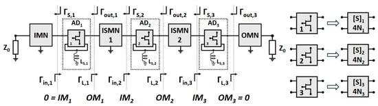
Figure 1.
(Left): Three-stage LNA schematic where reflection coefficients are reported at all sections with the corresponding mismatch values. The first and last mismatch values are set to ‘0’ to fulfill the signal match condition at the I/O ports of the 3-stage LNA. (Right): Electrical equivalence of the three transistors treated in terms of a linear scattering matrix and four noise parameters.
2.1. Active Device’s Input to Output Mismatch Relations
From this point forward, the active two-port network consisting of the FET with its source terminal connected to ground through an inductor () in Figure 1 (left) will be referred to as the ‘Active Device’ (AD). For simplicity, this manuscript assumes that the three transistors are identical—that is, they share the same small signal and noise parameters, while each transistor features a distinct value of inductive source degeneration. In practice, the three scattering matrices ([S]1, [S]2, [S]3) and noise parameters (4N1, 4N2, 4N3) shown in Figure 1 (right) correspond to those listed in Table 1. However, each Active Device is characterized by its own scattering matrix and noise parameters due to the different source degeneration inductors ().

Table 1.
FET small-signal and noise parameters at 28 GHz. The source terminal is ideally grounded.
The theoretical approach depends on the noise and small-signal parameters of each transistor, as will be shown later in the equations. Therefore, any changes in the transistors, such as geometry or bias points, will result in new noise and small-signal parameters that can be incorporated into the equations. Hence, the approach remains fully valid when different transistors are used (with varying geometries and/or bias points) in the three-stage LNA. In such cases, it is preferable to arrange the transistors so that their noise measure increases progressively from the first stage to the last.
It is worth noting that the transistor model based on [S] and 4N is fully representative of the physical transistor at the considered bias point. As a result, all parasitic effects—such as drain-to-gate feedback and contact impedance—are inherently accounted for. In this sense, the transistor is accurately modeled.
Here, and throughout the remainder of the manuscript, we assume that the input reflection coefficients of all stages () are chosen to satisfy the optimum noise condition as defined by Adler and Haus in [18], as this choice enables minimization of the noise figure (NF) in a multi-stage amplifier.
In the proposed analysis, the LNA transducer gain is expressed as a function of the two mismatch levels at the input and output terminals of the second stage active device, and , as shown in Figure 1 (left). The equations used to determine these mismatch levels are provided in (3) and (4). It is therefore essential to recall the definition of mismatch extensively used throughout this manuscript, as well as to present the relationship that links the input and output mismatch levels at the terminals of the active device. The input and output reflection coefficients of the active device, and , respectively—also illustrated in Figure 1—are defined in Equations (1) and (2), under the assumption of an optimum noise input termination, i.e., .
where is the determinant of the matrix of the S-parameters of the k-th active device , while the equation for the optimum noise input termination can be found in [19]. is the termination of the load in the k-th stage, as appears in Figure 1, and k ranges from 1 to 3.
Referring to Figure 1, the mismatch levels at the input () and output () terminals of each active device are defined in [20] and here recalled for the reader’s convenience.
where k ranges from one to three.
Mismatch levels can be interpreted in the following way: implies a perfect input conjugate signal match, (). is a controlled mismatch (). means a purely reactive input reflection coefficient (), and no active power is delivered from the source to the load. Meanwhile, is a condition in which the input reflection coefficient exhibits a negative real part (). The equivalent interpretation holds for and (). At a certain frequency, for the amplifier to be stable, the magnitudes of the reflection coefficients, () and (), must be less than unity for all passive source and load impedances. That is, and guarantee the conditional stability at the design frequency [21].
Essentially, the two relations (3) and (4) are functions of —directly in (4) and indirectly through in (3). Geometrically, Equations (3) and (4) represent two circles plotted in the output load plane. The formulas for computing the centers and radii of these circles are provided in [20]. An example of such input and output mismatch circles plotted in the load plane is shown in Figure 2.
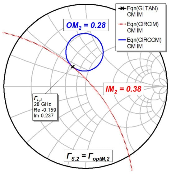
Figure 2.
Constant input (red dotted line) and output (blue solid line) mismatch circles in the output load plane for the second active device, plotted for at 28 GHz, when the input reflection coefficient is fixed for optimum noise behavior. The ‘x’ symbol is a tangency condition, therefore satisfying both mismatch conditions. Equations for the center and radius of the two mismatch circles are provided in [20].
The data are derived from the transistor’s S-parameter matrix and the four noise parameters (4N) listed in Table 1, with a 55 pH inductor inserted between the transistor’s source terminal and ground. This configuration applies series/series feedback while enforcing an optimum noise match at the input terminal. It should be noted that the tangency point shown in Figure 2 represents an optimum termination, as it simultaneously satisfies both mismatch conditions while minimizing their values.
The radii of the two circles shown in Figure 2 are proportional to the respective levels of mismatch [20]. Consequently, reducing one mismatch level under the tangency condition results in an increase in the other. In this context, a trade-off between the and levels becomes necessary.
An example of the versus trade-off at the input/output terminals of the second-stage () active device is illustrated in Figure 3, where the source feedback inductance value, , is varied. Changing the inductance value affects both the linear and noise parameters of the active device, as extensively discussed in the open literature [22]. For a specific segment (i.e., a particular source degeneration value), the trade-off between and is achieved by adjusting the output termination , while keeping the input termination fixed at .
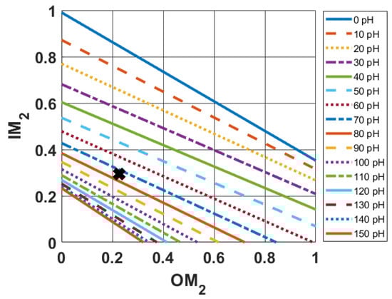
Figure 3.
The second stage’s vs. mismatch levels when sweeping the values of . Each segment is generated by imposing and adjusting the load termination to fulfill a specific tangency condition, exemplified in Figure 2, for every value. The black ‘x’ symbol indicates the position of the - pair for the reader’s convenience.
The negative slope observed in Figure 3 illustrates that improving the mismatch level at one terminal of the transistor comes at the expense of increased mismatch at the other terminal. The overall trade-off can be optimized by adjusting the source feedback inductance, although this comes at the cost of reduced available gain (or equivalently, the associated gain, since the input port of the active device is assumed to be terminated for optimum noise performance). As feedback inductance increases, the versus segments shift closer to the origin, indicating that lower values (i.e., improved) of and can be achieved simultaneously. In this sense, enhancing the trade-off between mismatches is possible by increasing feedback inductance, although at the cost of the associated gain of the active device.
To draw versus segments as shown in Figure 3, the value of is determined and fixed to for each feedback inductance value. The two end points of each segment, (, 0) and (0, ), can be determined using (5) and (6), as presented in [20].
Here, k ranges from one to three. MSG denotes the maximum stable gain of the active device, K is Rollet’s stability factor, and represents the associated gain—that is, the gain available when the source termination seen by the active device is configured for the optimum noise performance.
The value of represents the best (=lowest) output mismatch when the input is conjugately matched, while is the lowest input mismatch value when the output is conjugately matched. It is worth mentioning that the value under the square root cannot be negative since (5) and (6) represent a specific condition of the more general (3) and (4), which are nonnegative real values by definition.
2.2. Active Device’s Optimum Linear and Noise Terminations
Typically, the LNA input stage is designed to satisfy the simultaneous signal-and-noise match (SSNM) condition—that is, —while imposing an optimum noise termination at the input terminal (). As a consequence, the mismatch in the output of the first stage is , as recalled in the previous Section 2.1. The first stage load termination that agrees to satisfy the SSNM condition, mathematically expressed as , is defined as [20].
An analysis of the active device’s optimum linear and noise terminations is required before continuing with the design description. Figure 4 depicts three noteworthy linear and noise terminations of the active device while sweeping the feedback inductor from 0 to 150 pH in 10 pH steps.
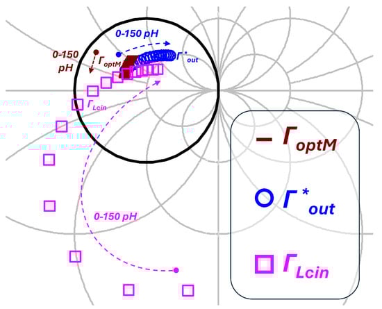
Figure 4.
The active device’s noteworthy linear and noise input and output terminations are calculated at 28 GHz. The feedback inductor is swept from 0 to 150 pH at 10 pH steps. The black circle indicates the unitary magnitude reflection coefficient locus.
The noise and linear parameters of the transistor are reported in Table 1. The notable linear and noise terminations depicted are the optimum input termination for noise (), the output termination that provides a conjugate match in the output section () when the input port is matched for noise, and finally the output termination that satisfies the SSNM condition () when the input port is matched for noise.
The data provided in Figure 4 show a behavior worth analyzing. First, the position of the optimum input termination for noise () appears to be slightly affected by the feedback inductor value. Second, in this specific case, presents a negative real part for feedback inductor values from 0 to approximately 60 pH. Consequently, passive load terminations can fulfill the SSNM condition only when the feedback inductor is greater than 58 pH. This corresponds to having larger than unity in Figure 3 for pH. Third, and draw close to each other as the feedback value increases. The condition and explains why source degeneration is applied to facilitate the trade-off between input and output matching in the first stage of a low-noise amplifier. This interpretation () is a more formal definition than the common explanation that source degeneration is applied to bring closer the available gain and noise figure circles in the input termination plane.
3. LNA Gain Versus Inter-Stage Mismatch Level Relations
Section 2.1 recalls how to calculate the mismatch levels at the I/O ports of the three active devices in the LNA. The same section describes how a specific mismatch pair (, ) is obtained using a specific triplet (, , ). Therefore, mismatch levels can be used to quantify the transducer gain of the three active devices in the LNA. Furthermore, Section 2.2 introduces the various notable reflection coefficients used in this study.
In this section, the procedure for obtaining a three-dimensional graph of the three-stage LNA transducer gain versus (, ) is presented.
A ‘special case’ is also presented when , allowing the simultaneous extraction of the transducer gain and the feedback inductor values across the three stages from a single chart.
The three-stage LNA is represented by the simplified schematic diagram shown in Figure 1 (left). The matching networks are the input matching network (IMN), the first and second inter-stage matching networks (ISMN1 and ISMN2, respectively), and the output matching network (OMN). In addition, embedding networks (i.e., , and ), which act as series/series feedback, are described in Figure 1.
To obtain a simultaneously I/O-matched three-stage LNA, the input section of the first stage and the output section of the third stage must be perfectly matched to the reference impedance, . Moreover, the input of all stages is matched for optimum noise behavior. A consequence of these two design choices (LNA I/O match and optimum input noise match on all stages) is that some signal mismatch level must be allowed at the inter-stage sections—therefore, at the terminals of ISMN1 and ISMN2. In this manuscript, we show that inter-stage mismatch levels can be adjusted to meet a specific gain level while maintaining the LNA I/O conjugate match and optimum noise behavior. The key point of the analysis is to choose the appropriate inductance value in each stage that results in the proposed mismatch and gain levels.
As stated previously, the input and output of the LNA are matched to ; this design choice corresponds to a perfect signal match at the LNA’s I/O ports expressed by the following relationships:
As we are assuming that the matching networks are designed with lossless and reciprocal elements (in practice, ideal inductors, capacitors, and/or transmission lines), the mismatch level at the I/O ports of all matching networks is identical. Mathematically, this hypothesis yields the following expression:
This means that in the first inter-stage matching network, ISMN1, the output mismatch level of the first stage is equal to the input mismatch level of the second stage, which implies the same for the second inter-stage matching network ISMN2. A consequence of the design choice expressed in (8) and the lossless hypothesis expressed in (9) is the following relationship:
All LNA mismatch levels are so defined. The LNA input and output mismatch levels are set to 0, to satisfy the matching condition, while the inter-stage matching levels ( and ) are used to determine the LNA gain. Such mismatch values are fulfilled by an appropriate synthesis of reflection coefficients and active device feedback inductor values.
The various terminations that fulfill the mismatch conditions expressed in (8) and (10) are reported in the following. All input terminations are synthesized to meet the optimum noise condition, while the three load terminations, and , are left to meet the prescribed mismatch level in the various sections. The final stage load termination, , shall equal , while the first stage load termination, , shall be equal to , as expressed in (7). Ultimately, the second stage load, , is synthesized imposing the desired mismatch condition at the I/O terminals of the second stage active device as graphically shown in Figure 2.
Regarding the LNA’s gain, having imposed and considering lossless matching networks, the transducer gain, , of the three-stage LNA can be calculated as follows:
where the associated gain, , is the available gain of the active device when its [23]. Regarding the LNA’s noise behaviour, we have imposed the condition that the input terminations of all transistors be synthesized to provide the optimum noise termination—i.e., . This design choice leads to a minimum LNA noise figure according to [8]. In fact, the theoretical minimum Noise Figure of an infinite cascade of optimally noise-matched transistors is [18], where is the minimum noise measure of the transistor at a specific bias point and is invariant to lossless embedding. Although a three-stage LNA is not an infinite cascade, we can assume that the figure of merit () represents an adequate approximation of the three-stage LNA’s NF, especially when the LNA gain is sufficiently high, for example, above 20 dB. If the resulting LNA NF is not satisfactory, the designer could try to improve it by tuning the bias point and/or modifying device geometry, obviously within the inherent capabilities of the selected technology.
Finally, the three feedback inductor values (that is, , and ) that allow for the fulfillment of the mismatch relations expressed in Equations (8) and (10) are determined using the charts provided in the following section.
3.1. Chart Preparation: Feasible Analysis Space
The FET used to provide the charts given in this section is modeled by the linear and noise parameters provided in Table 1. Therefore, the FET is not treated in a simplified manner and results from the characterization of a physical transistor.
To generate charts supporting the main claim, the reader should first follow these steps to identify the feasible design space.
Step 1: Equations (5) and (6) are applied to generate the plots in Figure 5 (left), that is, vs. and vs. . Subsequently, a numerical inversion is carried out and shown in Figure 5 (right) since we are interested in determining the feedback inductance value for a certain mismatch level. We limited the domain of numerical inversion to mismatch levels smaller than unity and considered the domain where the vs. and vs. curves display monotonic behavior. In this step, we also annotate the values of and .
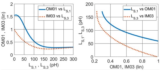
Figure 5.
(Left): vs. 1st and vs. 3rd stage’s feedback inductance and (right) the numerical inversion.
Step 2: Plot vs. functions while varying the feedback inductance of the second-stage active device, . The segments in Figure 3 are drawn using Equations (5) and (6) to identify the endpoints of each segment. The segments in the plot, as usual, are limited by mismatch values smaller than unity. The value of the pair and , annotated in the previous step, is marked as a black x for the reader’s convenience in Figure 3. It is interesting to note that the vs. segments tend to draw closer as the value of increases. Hence, further increasing the inductance value will not cause any improvement in the mismatch level; instead, it will worsen the associated gain as the inductance increases.
Step 3: A feasible design space is geometrically identified in the () plane by considering the following points:
- A
- ;
- B
- ;
- C
- ;
and the following lines:
- D
- vs. traced when pH;
- E
- ;
- F
- .
In the general case, such a figure will be an irregular pentagon that is obtained by juxtaposing a rectangular triangle whose hypotenuse lies in the segment identified by , two rectangles adjacent to the cathetes of such a rectangular triangle, and a final rectangle whose lower vertex is having sides coincident with the two adjacent rectangles. An example of a feasible design space in the () plane is shown in Figure 6.
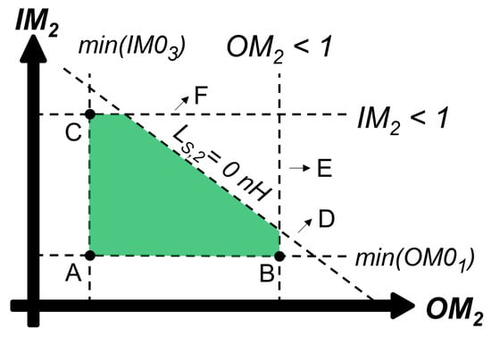
Figure 6.
Example of the feasible design space (colored area) for the proposed 3-stage LNA design.
3.2. LNA Gain vs. Intermediate Stage Mismatch Levels Chart
The transducer gain of the three-stage LNA versus (, ) can be derived using (9). In fact, fixing the mismatch levels at the I/O terminals of all active devices corresponds to fixing their source and load terminations and the values of the source feedback inductor. A practical way to obtain the graph, shown in Figure 7, is described in the following.
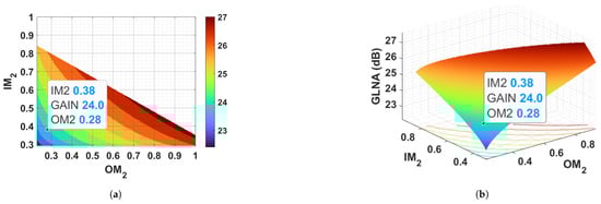
Figure 7.
(a): Three-stage LNA transducer gain vs. second-stage mismatch levels and at 28 GHz. (b): Three-dimensional surface representation—bottom: contour levels representation.
First: Discretize the - plane into a array. Increasing the number of points will increase the computation time, while improving the accuracy of the resulting plot. For the reader’s reference, the graph computation time is around 5 s for a 100 × 100 points array.
Second: For every point in the array, evaluate if the considered point (, ) lies inside or outside the feasible design space, schematically represented in Figure 6.
Third: If the considered point lies within the feasible design space, then it is necessary to determine the triplet associated with the considered point. and are readily available from the plots in Figure 5 (right), recalling the validity of (10). is obtained by identifying the vs. segment in Figure 3 closest to the considered (, ) point. Obviously, the interpolation error improves as the number of segments considered in Figure 3 increases, or, in other words, as steps become smaller. No operation is performed if the considered point (, ) is not within the feasible design space.
Fourth: For the points lying inside the feasible design space, the total transducer gain of the three-stage LNA, , can now be calculated using (9), since the triplet is determined for the specific point , and so are the source and load terminations at all stages.
The resulting graph is provided in Figure 7. The counterintuitive behavior that a higher LNA gain is obtained through a higher mismatch between stages is highlighted in Figure 7. This is the consequence of imposing lower feedback on the second stage transistor to obtain a higher stage gain. In fact, it is not necessary to fulfill a signal matching condition at the terminals of the second device, since it is an internal section. To validate this result, two practical three-stage LNA designs will be discussed in the following sections.
4. Practical Examples
Two practical LNA design examples are provided in the following sections to validate our main claim. The first example, more general, implies synthesizing different values of and . In the second example, more specificity is obtained by imposing . Higher inter-stage mismatch levels are imposed in the second case to prove the claim that higher LNA gain is obtained with higher inter-stage mismatch levels.
4.1. General Case, Any () Inside the Feasible Area
The general case is based on the assumption that any (, ) pair within the feasible area can be selected. In this case, the transducer gain chart is a 3D plot. To prove this case, the proposed gain level, as shown in Figure 7, is set to 24 dB. A possible level of mismatch in the intermediate section is (, ) = (0.28, 0.38) as seen in Figure 7.
The corresponding values of and are 129 pH and 114 pH, respectively, as can be determined from Figure 8, which is a zoomed-in version of Figure 5 (right) to help the reader better assess the values.
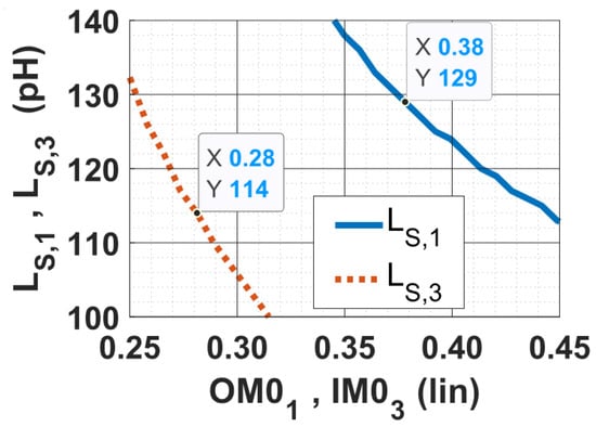
Figure 8.
Zoomed-in version of Figure 5 for and .
The value of is 55 pH as can be read from the graph in Figure 9, which is essentially a zoomed-in area of Figure 3 around the point considered .
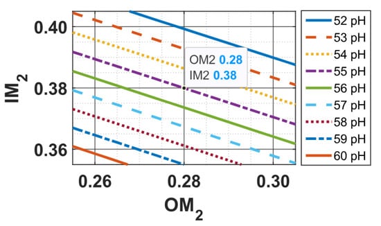
Figure 9.
Zoomed-in version of Figure 3 around (, ) = (0.28, 0.38).
Table 2 and Table 3 present the main design parameters. In particular, Table 2 contains the feedback values required to obtain an I/O match to 50 in the I/O ports of the LNA and (, ) = (0.28, 0.38) in the intermediate section of the LNA, while Table 3 contains the source reflection coefficients at all sections that implement the specific design choice. As usual, the input terminations are selected to fulfill an optimum noise measure termination.
Table 2.
Input and output mismatch levels and corresponding inductance values for each active device at 28 GHz for (, ) = (0.28, 0.38).
Table 3.
Optimum noise measure terminations and corresponding associated gain for the three active devices at 28 GHz when (, ) = (0.28, 0.38).
The output loads are synthesized with the following criteria: implements , implements , and implements the condition (, ) = (0.28, 0.38), as seen in Figure 2. The required load terminations on each stage are provided in Table 4. The three-stage LNA schematic with the ideal elements that implement this configuration is provided in Figure 10.
Table 4.
and noteworthy load terminations for the three active devices at 28 GHz for (, ) = ().
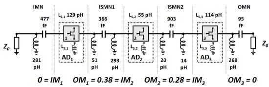
Figure 10.
The ideal element schematic for the 3-stage LNA when yielding 24 dB of LNA gain.
The technology selected for the MMIC demonstration is the Gallium Arsenide PIH1-10 from the WIN Foundry, which provides an acceptable trade-off between adequate noise performance and technological maturity [24]. The PIH1-10 process integrates monolithic PIN diodes, capable of power switching up to 50 GHz, into an advanced 100 GHz pseudomorphic HEMT platform. This technology provides advanced transmit power performance and a lower receiver noise figure, which are requirements for 5G systems.
An evaluation of the geometry of the transistor and the bias point is performed to determine the optimum geometry configuration and bias point for low-noise and high-gain performance. The outcome of the analysis is a µm FET biased at V and mA/mm. The transistor’s small-signal and noise parameters at the selected bias point are provided in Table 1.
For this device, is calculated to be 0.465, which corresponds to an NF of 1.66 dB of an infinite cascade of identical stages designed with lossless embedding. In practice, the cumulative Noise Figure is unchanged after the third stage, when the cumulative gain exceeds 20 dB. However, in the practical case, the designer has to account for at least the losses of the input matching network and the source degeneration.
The MMIC implementing the circuit reported in Figure 10 is shown in Figure 11 where the inductive dipoles are synthesized through thin microstrip lines of appropriate length.
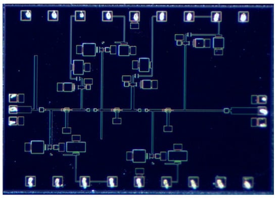
Figure 11.
Micro-photograph of the realized 3-stage LNA MMIC test vehicle for the proposed design. The chip size is 3.0 mm × 2.0 mm and manufactured in WIN foundry’s PIH1-10 technology.
The MMIC S-parameters are measured by an HP8510C Vector Network Analyzer from Hewlett Packard, from 100 MHz to 40.1 GHz at 100 MHz intervals, while the Noise Figure measurement is performed with an Agilent E4448A Power Spectrum Analyzer preamplified by two LNAs. The EM simulated and measured results are reported in Figure 12.
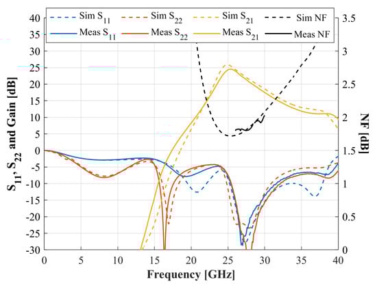
Figure 12.
Demonstrator MMIC’s measured (solid lines) and simulated (dashed lines) s-parameters and NF.
The simulated values are in good agreement with the characterized data. This aspect entails the validity of the active device model and the simulation method of the passive structures (EM simulations using AWR’s AXIEM simulation engine). The LNA is optimally signal-matched around 28 GHz, since the I/O return loss is better than 23 dB. The MMIC’s measured gain is around 21.5 dB. The difference between theoretical and measured gain is mainly due to the resistive losses of the embedding networks. A similar consideration holds for the difference between the NF of the ideal lossless LNA (1.55 dB) and the measured MMIC NF (1.85 dB).
4.2. Special Case, When Within the Feasible Design Area
For this special case, the selected design point in Figure 13 is a gain of 26 dB, corresponding to , which is higher than the values used in the previous case (0.38, 0.28).
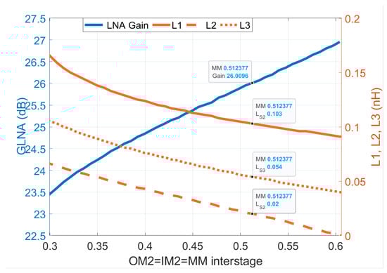
Figure 13.
Chart when at 28 GHz. LNA transducer gain is plotted on left axis, while three feedback inductor values can be read on right axis. Markers are given for 26 dB gain value.
From Figure 13, the values of , , and can be read to be 103, 20, and 54 pH, respectively. The geometry of the transistor and the bias point used to generate the graph in Figure 13 is the same as in the previous case. Figure 13 also shows that LNA gain is proportional to mismatch level. To obtain this behavior, the feedback inductor values must decrease to implement higher LNA gain.
The corresponding ideal-element LNA schematic is provided in Figure 14, while the values of the reflection coefficients in all sections are given in Table 5.
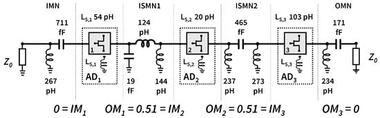
Figure 14.
The schematic for the LNA when , yielding 26 dB LNA gain.
Table 5.
Input and output reflection coefficients and corresponding associated gain for the three active devices at 28 GHz when .
5. Results and Discussion
The proposed claim is that a higher LNA gain is obtained when higher inter-stage mismatch values are selected. In turn, these higher mismatch values are a consequence of lower feedback inductance values (), as appears in the schematic reported in Figure 10 and Figure 14 and more clearly in the chart proposed in Figure 13.
The graphs presented in Figure 7 and Figure 13 allow the designer to start synthesizing an optimum noise and signal-matched three-stage LNA with a prescribed transducer gain level, , at a single frequency point. Practically, the designer must trade off between the two inter-stage mismatch values ( and ) and the desired LNA transducer gain .
The input terminations on all stages are selected to meet an optimum noise measure match condition, and the output terminations are left to satisfy a vs. trade-off. The proposed method optimizes this trade-off since the load termination is selected to provide the lowest for a given value or vice versa. This optimum selection is represented graphically by the tangency condition shown in Figure 2. In other words, once the source feedback inductor is fixed, any load termination other than the determined one will not improve the LNA gain and noise performance, but will worsen the mismatch level in the considered section.
This analysis is based on the linear and noise parameters of the transistor. Consequently, the FET is accurately modeled and all parasitic and feedback effects are taken into account. Admittedly, the only ideal assumption here treated is (9), that is, considering lossless and reciprocal matching networks. The validity of this assumption diminishes at higher frequencies or when the topology of the matching networks becomes more complex.
Finally, in-band stability is taken into account at design frequency since all sections mismatch levels are imposed to be smaller than unity [21,25] guaranteeing at the very least conditional stability.
The MMIC demonstrator features a 10 dB I/O return loss bandwidth of 5.5 GHz, corresponding to approximately 20% relative bandwidths. Therefore, this analysis is not a broadband LNA design procedure, but it is an insight into the controlled transducer gain of the LNA by the inter-stage mismatch levels. The hypothesis has been verified through two design examples of three-stage LNA.
6. Conclusions
The objective of this study is to highlight the role of inter-stage mismatch levels in controlling transducer gain in optimally noise- and signal-matched LNAs. This objective is fulfilled by introducing for the first time novel charts for three-stage LNAs in which the gain is readily available as a function of inter-stage mismatch levels.
These charts can be a starting point for the synthesis of a three-stage LNA with optimum input/output signal matching and minimal noise figure while fulfilling a predetermined gain level at a specific nominal frequency. The procedure is optimum, which means that the NF is minimized and the I/O ports are matched to the normalization impedance, . The gain level essentially depends on the three-stage topology architecture and obviously the limits of the technology, but at least can be determined beforehand.
Once again, this study cannot be adopted as a three-stage LNA wideband design procedure since it relies on a single frequency, resulting in a non-flat gain curve as can be shown in Figure 12. However, this analysis could be a starting point that gives insight into a deterministic approach, meaning that a direct solution can be implemented to avoid designers featuring a laborious trial-and-error process.
In conclusion, the role of inter-stage mismatch levels is highlighted and discussed, showing that a higher gain is obtained at the expense of higher inter-stage mismatch levels. The method reported in this manuscript overcomes an intrinsic limitation of the arbitrary N-stage LNA design method proposed in [17], where the gain level is calculated only after the mismatch levels are synthesized, as opposed to the case presented here for , where the gain is readily available in the graph. Finally, a Ka-band MMIC implementation of the three-stage LNA is carried out to verify the proposed methodology.
Author Contributions
Conceptualization, P.E.L.; methodology, F.A. and P.E.L.; software, F.A. and P.E.L.; validation, W.C., S.C., A.S. and E.L.; formal analysis, F.A. and P.E.L.; investigation, W.C., S.C. and A.S.; resources, P.E.L.; data curation, F.A. and P.E.L.; writing—original draft preparation, F.A.; writing—review and editing, P.E.L.; visualization, F.A. and P.E.L.; supervision, P.E.L. and E.L.; project administration, P.E.L. and E.L.; funding acquisition, P.E.L. and E.L. All authors have read and agreed to the published version of the manuscript.
Funding
This research received no external funding.
Data Availability Statement
Data are contained within the article.
Acknowledgments
The demonstrator MMIC in PIH1-10 technology described here is realized by WIN Semiconductors within the “select university” program for the Microwave Engineering Center for Space Applications (MECSA). In particular, the authors are grateful to David Danzilio and the WIN Customer Engineering Department for their support. They would also like to thank Filippo Bolli and Enzo De Angelis for their support in characterizing the low-noise amplifier.
Conflicts of Interest
The authors declare no conflicts of interest.
References
- Ragonese, E.; Scuderi, A.; Palmisano, G. A 0.13-µm SiGe BiCMOS LNA for 24-GHz Automotive Short-Range Radar. In Proceedings of the 2008 38th European Microwave Conference, Amsterdam, The Netherlands, 27–31 October 2008; pp. 1537–1540. [Google Scholar] [CrossRef]
- Limiti, E.; Colangeli, S.; Bentini, A.; Ciccognani, W. Robust GaN MMIC Chipset for T/R Module Front-End Integration. Int. J. Microw. Opt. Technol. 2014, 9, 6–13. [Google Scholar]
- Bettidi, A.; Carosi, D.; Cetronio, A.; Corsaro, F.; Costrini, C.; Lanzieri, C.; Marescialli, L. X-Band transmit/receive module MMIC chip-set based on emerging GaN and SiGe technologies. In Proceedings of the 2010 IEEE International Symposium on Phased Array Systems and Technology, Waltham, MA, USA, 12–15 October 2010; pp. 250–255. [Google Scholar] [CrossRef]
- Limiti, E.; Ciccognani, W.; Cipriani, E.; Colangeli, S.; Colantonio, P.; Palomba, M.; Florian, C.; Pirola, M.; Ayllon, N. T/R modules front-end integration in GaN technology. In Proceedings of the 2015 IEEE 16th Annual Wireless and Microwave Technology Conference (WAMICON), Cocoa Beach, FL, USA, 13–15 April 2015; pp. 1–6. [Google Scholar] [CrossRef]
- Montazeri, S.; Bardin, J.C. A 2–4 GHz Silicon Germanium Cryogenic Low Noise Amplifier MMIC. In Proceedings of the 2018 IEEE/MTT-S International Microwave Symposium-IMS, Philadelphia, PA, USA, 10–15 June 2018; pp. 1487–1490. [Google Scholar] [CrossRef]
- Montazeri, S.; Wong, W.T.; Coskun, A.H.; Bardin, J.C. Ultra-Low-Power Cryogenic SiGe Low-Noise Amplifiers: Theory and Demonstration. IEEE Trans. Microw. Theory Tech. 2016, 64, 178–187. [Google Scholar] [CrossRef]
- Albinsson, B. A graphic design method for matched low-noise amplifiers. IEEE Trans. Microw. Theory Tech. 1990, 38, 118–122. [Google Scholar] [CrossRef]
- Engberg, J. Simultaneous Input Power Match and Noise Optimization using Feedback. In Proceedings of the 1974 4th European Microwave Conference, Montreux, Switzerland, 10–13 September 1974; pp. 385–389. [Google Scholar] [CrossRef]
- Güneş, F.; Demirel, S.; Özkaya, U. A low-noise amplifier design using the performance limitations of a microwave transistor for the ultra-wideband applications. Int. J. RF Microw. Comput. Aided Eng. 2010, 20, 535–545. [Google Scholar] [CrossRef]
- Corral, C.A. Design of microwave transistor amplifiers with optimum cascaded gain and noise. IET Microw. Antennas Propag. 2016, 10, 1196–1203. [Google Scholar] [CrossRef]
- Heinz, F.; Thome, F.; Leuther, A. Monolithically Integrated C-Band Low-Noise Amplifiers for Use in Cryogenic Large-Scale RF Systems. IEEE Trans. Microw. Theory Tech. 2023, 72, 2442–2451. [Google Scholar] [CrossRef]
- Parveg, D.; Varonen, M.; Kantanen, M. A Full Ka-Band GaN-on-Si Low-Noise Amplifier. In Proceedings of the 2020 50th European Microwave Conference (EuMC), Utrecht, The Netherlands, 12–14 January 2021; pp. 1015–1018. [Google Scholar] [CrossRef]
- Fung, A.; Samoska, L.; Bowen, J.; Montanez, S.; Kooi, J.; Soriano, M.; Jacobs, C.; Manthena, R.; Hoppe, D.; Akgiray, A.; et al. X- to Ka- Band Cryogenic LNA Module for Very Long Baseline Interferometry. In Proceedings of the 2020 IEEE/MTT-S International Microwave Symposium (IMS), Los Angeles, CA, USA, 4–6 August 2020; pp. 189–192. [Google Scholar] [CrossRef]
- Varonen, M.; Reeves, R.; Kangaslahti, P.; Samoska, L.; Kooi, J.W.; Cleary, K.; Gawande, R.S.; Akgiray, A.; Fung, A.; Gaier, T.; et al. An MMIC Low-Noise Amplifier Design Technique. IEEE Trans. Microw. Theory Tech. 2016, 64, 826–835. [Google Scholar] [CrossRef]
- Kooi, J.W.; Soriano, M.; Bowen, J.; Abdulla, Z.; Samoska, L.; Fung, A.K.; Manthena, R.; Hoppe, D.; Javadi, H.; Crawford, T.; et al. A Multioctave 8 GHz–40 GHz Receiver for Radio Astronomy. IEEE J. Microw. 2023, 3, 570–586. [Google Scholar] [CrossRef]
- Schleeh, J.; Moschetti, G.; Wadefalk, N.; Cha, E.; Pourkabirian, A.; Alestig, G.; Halonen, J.; Nilsson, B.; Nilsson, P.Å.; Grahn, J. Cryogenic LNAs for SKA band 2 to 5. In Proceedings of the 2017 IEEE MTT-S International Microwave Symposium (IMS), Honololu, HI, USA, 4–9 June 2017; pp. 164–167. [Google Scholar] [CrossRef]
- Longhi, P.E.; Pace, L.; Colangeli, S.; Ciccognani, W.; Limiti, E. Novel Design Charts for Optimum Source Degeneration Tradeoff in Conjugately Matched Multistage Low-Noise Amplifiers. IEEE Trans. Microw. Theory Tech. 2021, 69, 2531–2540. [Google Scholar] [CrossRef]
- Haus, H.A.; Adler, R.B. Circuit Theory of Linear Noisy Networks; The MIT Press: Cambridge, MA, USA, 1959. [Google Scholar] [CrossRef]
- Poole, C.; Grammenos, R. Correct Equations for Minimum Noise Measure of a Microwave Transistor Amplifier. IEEE Trans. Microw. Theory Tech. 2022, 70, 1361–1366. [Google Scholar] [CrossRef]
- Ciccognani, W.; Longhi, P.E.; Colangeli, S.; Limiti, E. Constant Mismatch Circles and Application to Low-Noise Microwave Amplifier Design. IEEE Trans. Microw. Theory Tech. 2013, 61, 4154–4167. [Google Scholar] [CrossRef]
- Boglione, L.; Webster, R.T. Unifying interpretation of reflection coefficient and smith chart definitions. IET Microw. Antennas Propag. 2011, 5, 1479–1487. [Google Scholar] [CrossRef]
- Lehmann, R.E.; Heston, D.D. X-Band Monolithic Series Feedback LNA. IEEE Trans. Microw. Theory Tech. 1985, 33, 1560–1566. [Google Scholar] [CrossRef]
- Allen, J.W. Gain Characterization of the RF Measurement Path; National Telecommunications and Information Administration: Washington, DC, USA, 2004.
- Danzilio, D. Advanced GaAs Integration for Single Chip mmWave Front-Ends. Microw. J. 2018, 61, 148–156. [Google Scholar]
- Kurokawa, K. Power Waves and the Scattering Matrix. IEEE Trans. Microw. Theory Tech. 1965, 13, 194–202. [Google Scholar] [CrossRef]
Disclaimer/Publisher’s Note: The statements, opinions and data contained in all publications are solely those of the individual author(s) and contributor(s) and not of MDPI and/or the editor(s). MDPI and/or the editor(s) disclaim responsibility for any injury to people or property resulting from any ideas, methods, instructions or products referred to in the content. |
© 2025 by the authors. Licensee MDPI, Basel, Switzerland. This article is an open access article distributed under the terms and conditions of the Creative Commons Attribution (CC BY) license (https://creativecommons.org/licenses/by/4.0/).