Article

Impact of Electromagnetic Pulses on N-Type MOSFET Reliability: Experimental Insights

1
Beijing Smartchip Microelectronics Technology Co., Ltd., Beijing 102200, China
2
EMC Laboratory, Beijing University of Aeronautics and Astronautics, Beijing 100191, China
*
Author to whom correspondence should be addressed.
Electronics 2025, 14(10), 1937; https://doi.org/10.3390/electronics14101937
Submission received: 3 March 2025 / Revised: 27 April 2025 / Accepted: 9 May 2025 / Published: 9 May 2025
(This article belongs to the Special Issue Advanced High-Performance Analog Integrated Circuits)

Abstract

:
In power systems, MOSFET devices used in industrial chips exhibit more pronounced degradation when subjected to intense electromagnetic pulses than in conventional environments. Conventional reliability testing methods, which fail to simulate dynamic electromagnetic environments, are unable to accurately assess the changes in device performance under electromagnetic interference. In this study, we employed a transmission line pulse generator to apply pulse stress to N-type MOSFET devices, systematically investigating the degradation mechanisms by varying pulse features such as pulse cycle, amplitude, rise/fall times, and intervals. The results indicate that changes in the electrical properties of the devices are primarily influenced by two types of charged traps. Under the conditions of low pulse cycles, the current response of the devices may even exceed that prior to stress application. The study further analyzed the competitive mechanisms of these different traps during the device degradation process. Additionally, by varying the test temperature to mimic industrial application scenarios, we analyzed the degradation behavior of the devices under multi-physics conditions.

1. Introduction

The advancements of smart grid systems have driven the demand for efficient multimodal data processing and conversion at intelligent fusion terminals [1,2]. These terminals are often deployed near primary power equipment, where the electromagnetic environment is complex and harsh [3,4,5]. Terminal failures caused by electromagnetic disturbance (EMD) are frequent, with chip failures being an important concern [6]. Generally, EMD propagates through the chip pins, leading to degradation of electronic components, and hence, significantly affecting the safe and stable operation of power equipment.
Metal Oxide Semiconductor Field-Effect Transistors (MOSFETs) are of importance, as they constitute the functional units in the CPU and memory chips. In most cases, chip failures can be attributed to transistor degradation [7]. Prior to integration, reliability tests must be conducted to effectively evaluate the lifetime of MOSFETs. A conventional reliability test involves constant voltage stress or gradient stress for accelerated experiments, where voltage stress is systematically applied to the electrodes of MOSFETs to investigate changes in their electrical performance over varied stress durations [8,9]. Under severe EMD, the terminals of MOSFETs are subjected to electromagnetic stress from the environment, accelerating the degradation process and complicating the evaluation of device degradation [10,11,12]. In addition, EMD casts a more significant impact on emerging semiconductor devices, such as ferroelectric MOSFETs. Ferroelectric materials in these devices are particularly susceptible to hysteresis under high electric fields, which introduces unstable nonlinearities between the device gate voltage and internal potential, ultimately compromising the long-term reliability of the device [13].
In power systems, EMD mainly originates from transient electromagnetic pulses generated by equipment like high-voltage switchgear [14,15]. The pulses typically consist of pulse groups resulting from multiple discharge events or breakdowns, with frequencies ranging from 100 kHz to 100 MHz and pulse widths from 10 ns to 10 μs. Such pulses can pass through electrostatic discharge circuits and propagate to the MOSFET terminals [16]. In this study, we revealed the destructive impact of EMD pulses on switching MOSFETs, which are fabricated via typical BCD process. A transmission line pulse (TLP) generator was used to apply square pulses to the gate of the device, for the purpose of EMD simulation. The testing process innovatively incorporated engineering characteristic data to experimentally define the multi-physics environment of the device, enabling the design of a series of reliability tests that replicate real industrial conditions. The degradation of the device was then investigated, by examining the deviation of transfer characteristics. Changes in threshold voltage and mobility were analyzed to reveal the competitive mechanisms of Si–H and Si–O bond breakage in modulating device behavior. A distinct threshold voltage reduction had been observed under a small number of pulse impacts. The degradation of MOSFETs under multi-physics conditions was also elucidated, covering extreme temperatures ranging from −50 °C to 125 °C.

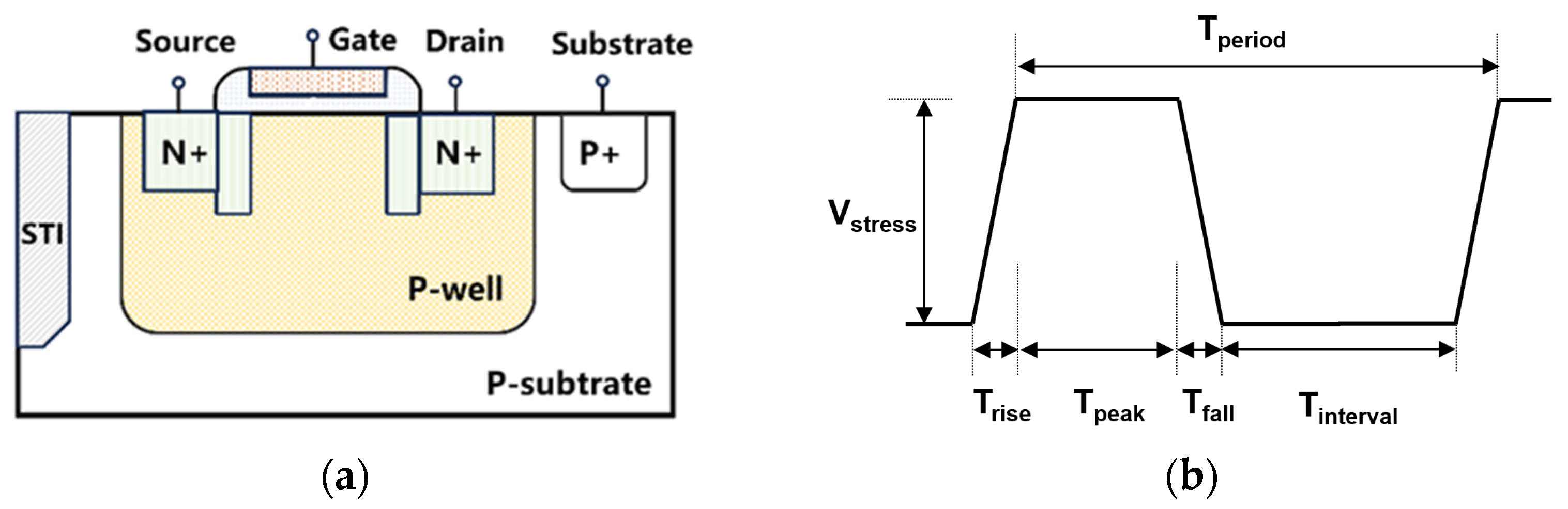
2. Materials and Methods
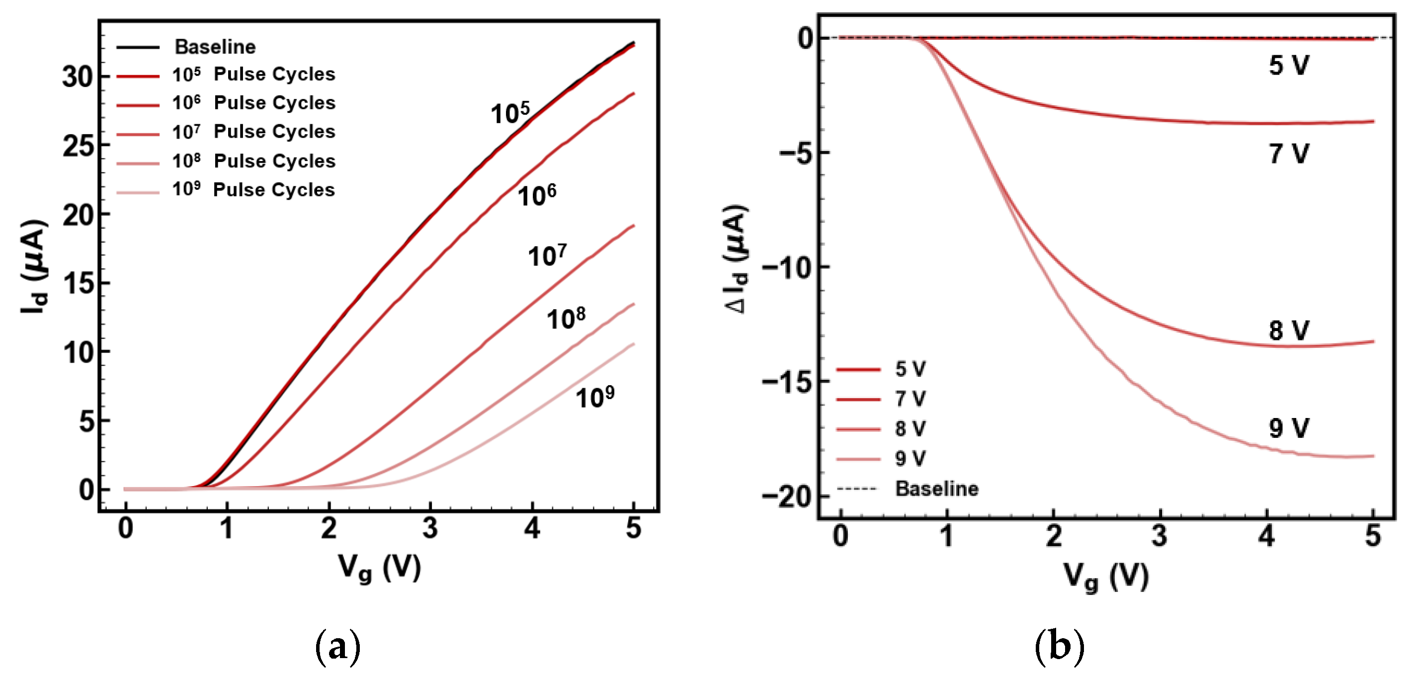
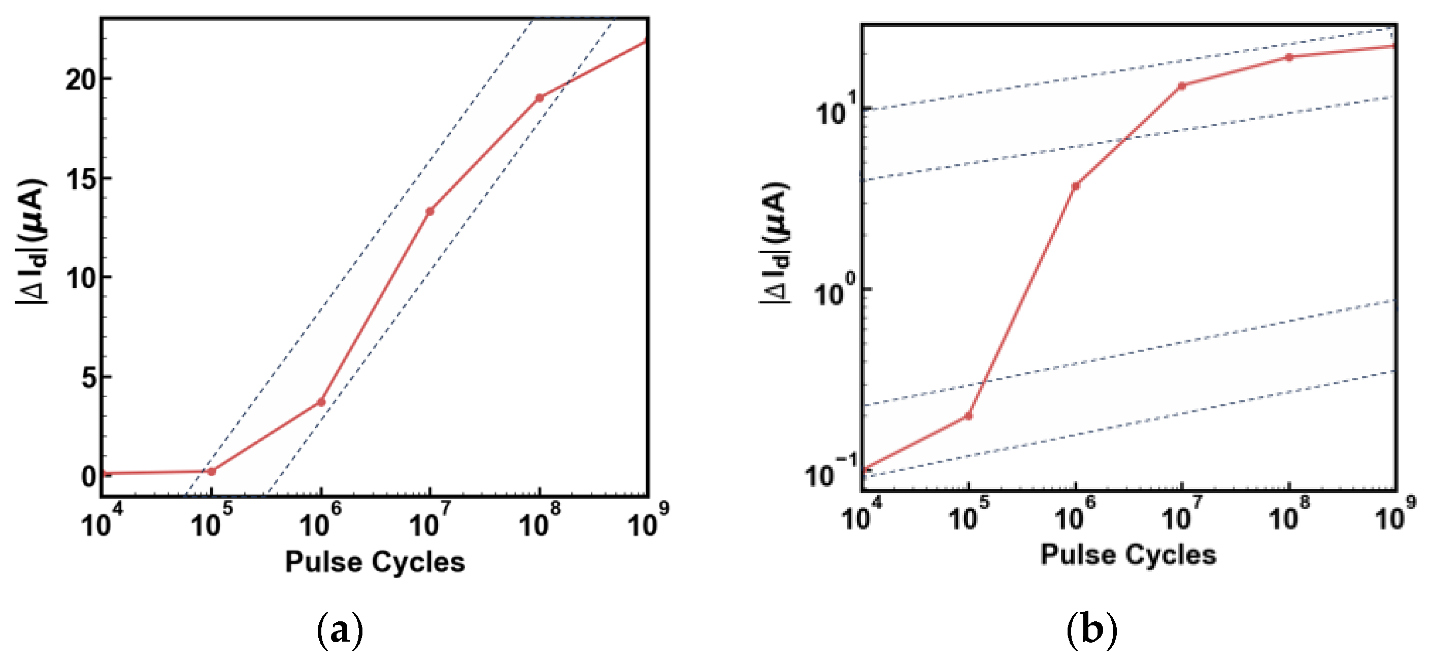
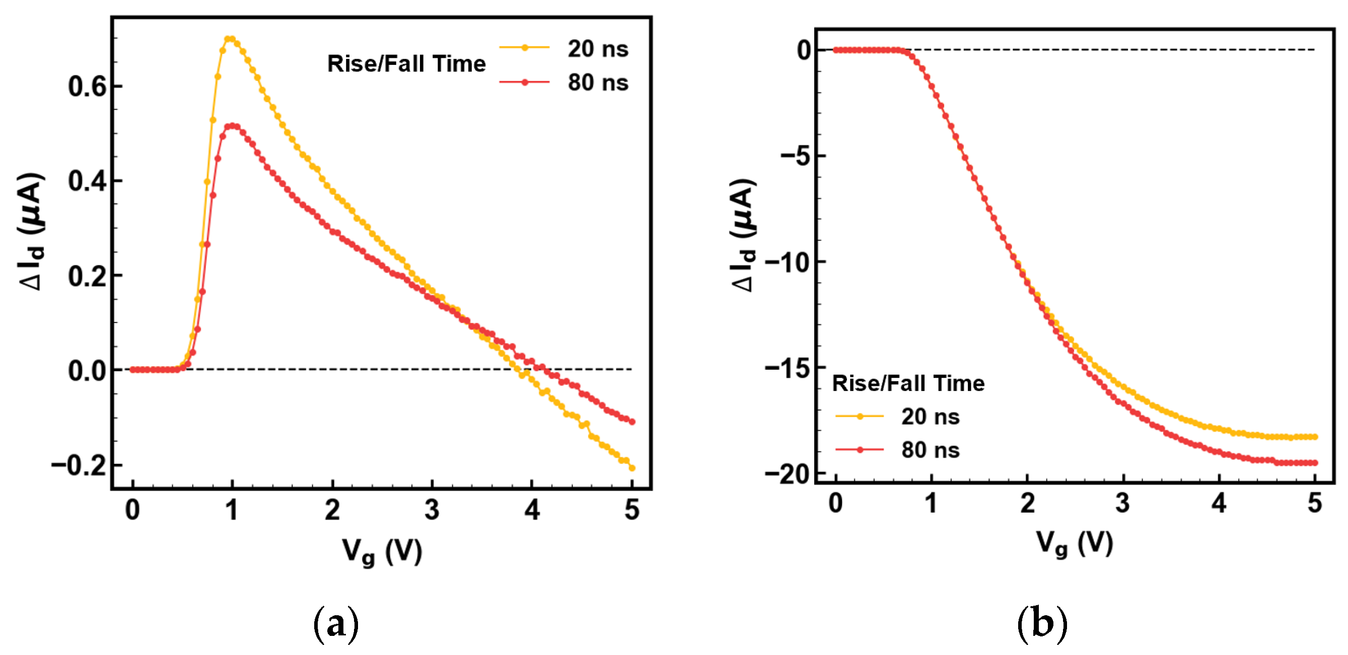
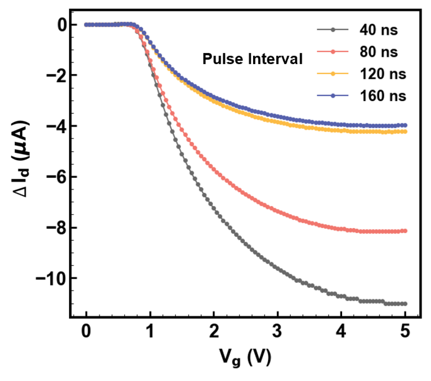
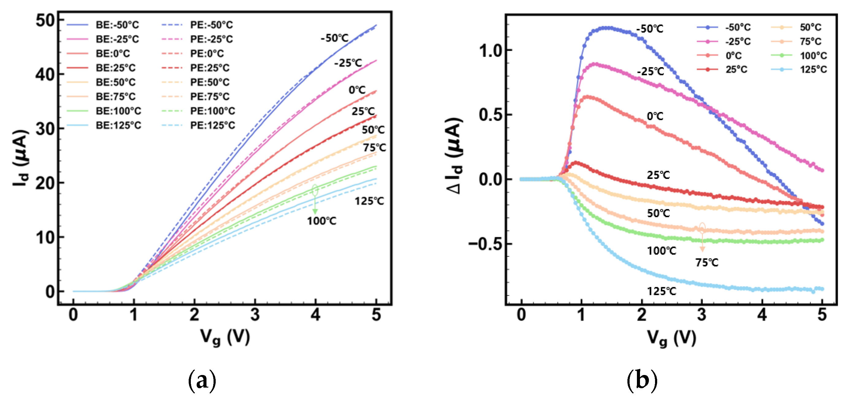
Standard 5 V N-type MOSFETs (NMOSs), fabricated via a traditional BCD process, were prepared for the experiments. The device structure is illustrated in Figure 1a. The substrate thickness is 775 μm. The channel length and width of the device are 1.2 μm and 10.0 μm, respectively. A reverse-doped well structure is adopted, with Boron implantation concentrations of 1013 cm−3, 1.5 × 1013 cm−3, and 2.4 × 1012 cm−3, separately. To mitigate the electric field distribution, the lightly doped drain (LDD) structure is carefully designed, with a Phosphorus concentration of 2.3 × 1013 cm−3. The source and drain of the device are doped with Phosphorus at 1.5 × 1014 cm−3 and Arsenic at 4.5 × 1015 cm−3. The depths of the drain/source, LDD, and well are measured as 32.6 nm, 69.0 nm, and 261.8 nm, respectively, while the thickness of the gate oxide and poly-silicon layer are 14.5 nm and 200.0 nm, respectively.
After tape-out, the fabricated devices were placed in a cryostat to ensure precise and stable temperature control for the reliability tests. Multiphysics experiments were then conducted. Periodic square pulses were applied to the gate of the devices using a TLP system (ES622, ESDEMC Technology, Rolla, MO, USA), with the pulse waveform shown in Figure 1b. A schematic diagram of the experimental setup is illustrated in Figure 2, where the function of each component can be found in Table 1. Given that the gate breakdown voltage of MOSFETs was measured to be 12 V, pulses with an amplitude (Vstress) ranging from 5 V to 11 V were specified during the experiments. To explore the impact of waveforms on device degradation, the duration and duty cycle of the periodic pulses were varied. Experimental details are listed in Table 2. Reliability tests were performed on devices under off-state condition, followed by an evaluation of the resulting variations in their DC output characteristics.

3. Results

The reliability of NMOS devices was first evaluated at room temperature, with varied pulse amplitudes and cycles (Experiment No. 1). The rise and fall times (Trise and Tfall) were fixed at 20 ns, the pulse stress time (Tpeak) was set to 150 ns, and the pulse period (Tperiod) was maintained at 350 ns. Figure 3a shows the degradation of the device’s transfer characteristics (IdVg) at Vstress = 8 V. As the pulse cycles increase from 10⁵ to 10⁹, the drain current gradually decreases, accompanied by an increase in the threshold voltage. This output performance degradation is primarily attributed to carrier injection across the Si–O interface. When electrical pulses reach the gate terminal, electrons in the p-well are attracted by the perpendicular electrical field under the oxide. The electrons gain kinetic energy and penetrate into the oxide layer through field-driven processes such as Poole–Frenkel emission. This energetic injection leads to the breakage of Si–O bonds in the oxide matrix. The resulting broken bonds create charged trap states that subsequently influence carrier transport when the device works, either enhancing carrier scattering in the channel or inducing severe recombination at the interface. Consequently, the drain current is diminished and threshold voltage can be elevated [17,18]. Note that there is a slight current improvement when only 105 pulses are applied to the device, indicating a decrease in threshold voltage.
In Figure 3b, the effect of pulse voltage was analyzed across multiple samples (Experiment No. 2). Due to process variations, NMOS samples exhibit slight differences in performance [19,20]; only samples showing a threshold voltage fluctuation within 50 mV during the wafer acceptance test were selected for the experiment to avoid inconsistency of the results. The relative difference in drain current (ΔId) with respect to gate voltage (Vg) was used to evaluate the degradation, representing the drain current deviation between the post-stressed and pristine devices. At fixed 107 pulse cycles, an increase in Vstress from 5 V to 9 V leads to more severe degradation, demonstrating the positive correlation between stress intensity and device degradation. The stress amplitude of 5 V has been proven to cause no observable degradation in device performance, as it falls within the device’s normal operating range.
The current degradation trend in Figure 3a has been extendedly studied. Saturation currents are extracted from each curve at Vg = 5 V. The absolute change in drain current with respect to pulse cycles are shown in Figure 4. From the semi-logarithmic coordinate plot, it is evident that the current degrades logarithmically as pulse cycle increases. In general, degradation processes such as bias temperature instability and time-dependent dielectric breakdown follow power-law regarding time-dependent parameter evolution [7]. These mechanisms are typically associated with Si–H and Si–O bond breakage in the device, respectively. The observed logarithmic current change in the case suggests a more complex degradation mechanism within the device. The results presented in the logarithmic coordinate confirm this phenomenon. Two distinct regions following power-law dependencies are indicated by the dashed lines. Such findings suggest a change in the governing mechanism as the number of pulse cycles increases. Table 3 presents a theoretical comparison between commonly studied degradation topics and this work.
The effect of pulse cycles on the device output characteristics at different Vstress was further explicitly investigated (Experiment No. 3). To quantify the degradation, the shift in threshold voltage (ΔVth) was examined. The threshold voltage (Vth) was extracted from the transfer characteristics curve at the maximum transconductance and was measured as 0.67 V for 5 V NMOSs [24]. The results are shown in Figure 5a. It is evident that ΔVth is strongly correlated with both pulse cycles and Vstress, where a higher Vstress and an increased number of pulse cycles lead to more severe degradation. Notably, an inflection point in ΔVth is observed in the initial stress stage, where Vth first decreases at a few pulse cycles and then increases. The minima of ΔVth decreases with increasing Vstress and occurs at the lowest pulse cycle count when Vstress = 11 V. Reduced Vstress extends the negative shift in ΔVth over an increasing number of pulse cycles; however, the minima are barely detected under a Vstress of 7 V.
The increase in Vth is generally attributed to high-energy carrier injection into the gate oxide, as they can stay trapped in the oxide and break Si–O bonds at the Si/SiO2 interface, generating interface traps that capture electrons and introduce fixed negative charges. In contrast, the breaking of Si–H bonds should be responsible for the reduction in Vth [25]. In a typical BCD process, MOSFETs are usually treated with an annealing process to minimize surface dangling bonds through the formation of Si–H bonds [26,27]. These dangling bonds act as defects that can become positively charged. When carriers are injected into the oxide, relatively weak Si–H bonds can be broken, regenerating the dangling bonds and inducing positive fixed oxide charges. The observed inflection point arises from the trade-off between two competitive mechanisms.
Although the reduction in Vth enhances current outputs, traps accumulate in the device. For MOSFETs operating in the saturation region, the ideal current–voltage relationship can be derived as follows [24]:
I d = W μ n C O X 2 L V g V t h 2 ,
where W and L denote the device width and channel length, μ n is the carrier mobility, COX is the gate dielectric capacitance, and Vg represents the imposed gate voltage. The transconductance can be conducted as [24]:
g m = W μ n C O X L V g V t h
Given that the gate oxide thickness of fabricated device is 14.5 nm, COX is calculated using parallel-plate capacitor formula, yielding approximately 2.38 × 10⁻³ F/m2. In essence, since both interface traps and traps within the gate oxide layer are caused by impact carriers, the change trend of the dielectric constant of SiO2 is consistent with that of carrier mobility. To qualitatively analyze the mobility variation, it is assumed that the gate oxide capacitance of SiO2 remains unchanged. The carrier mobility is then determined by fitting the change of gm along with Vg [24]. The degradation of mobility is visualized in Figure 5b. It is clear that the mobility decreases monotonically with the increase in pulse cycles. In addition, the stronger the pulse voltage, the faster the mobility declines. The decrease in mobility originates from trap accumulation, where the monotonic tendency indicates the increasing trap concentration. The presence of the minima in Figure 5a can thus be further explained. The minimum Vth is found when 11 V pulses are imposed on the device, which results from the lower bond dissociation energy of Si–H bonds than that of Si-O bonds, leading to different accumulation rates of various types of traps [28]. Stronger pulse stress promotes the breaking of Si–H bonds, accelerating the accumulation of positive traps around the channel, which triggers Vth minima appearing at a lower pulse count. On the other hand, under 7 V stress, the Vth reduction benefiting from Si–H bond breaking is effectively balanced out, making it difficult to observe.
Considering the various pulse waveforms present in the EMD environment, the effect of Trise and Tfall of the pulses was explored (Experiment No. 4). Figure 6a,b illustrate the device’s output changes under pulses with different rise/fall edges for pulse cycles of 104 and 107, respectively, with a fixed pulse voltage of 9 V. After exposure to 104 pulses, an increase in device current due to Vth decrease is observed under both 20 ns and 80 ns pulse edge conditions. Compared to the experiment applying 20 ns edge pulses, the current increase is weaker when Trise = Tfall = 80 ns. This is due to the higher average electric stress of the latter case, giving rise to more Si–O bond breakage and additional negatively charged traps [7]. The overlap of curves near the saturation region suggests that the transfer curve obtained from the 20 ns-edge-pulse experiment is smoother under the influence of high perpendicular electric field around surface and, as discussed above, the device mobility decreases more significantly in this scenario. The reduction in device mobility is mainly attributed to the breaking of Si–H and Si–O bonds. Given that electron trapping and detrapping processes are more pronounced when positively charged traps are present, the device mobility is more significantly affected by Si–H bond breakage than by scattering caused by negatively charged traps originating from Si–O bonds. In this regard, a shorter pulse edge time appears more favorable for Si–H bond breakage. In light of the curve from the 80 ns-edge-pulse experiment, the formation of negatively charged traps due to Si–O bond breakage alters the electric field in the channel and seems to suppress Si–H bond breakage. For devices subjected to 107 pulses on the gate terminal, current degradation occurs under both conditions, with more severe degradation observed under 80 ns edge pulses due to the increased average electric stress level. Moreover, since Si–H bonds are limited at the device interface, the overall degradation can be mostly governed by the concentration of Si–O bond defects in this case [29,30].
Figure 7 reveals the effect of the pulse interval (Tinterval) on device degradation, with Vstress set to 9 V and pulse cycles set to 105 (Experiment No. 5). As Tinterval extends from 40 ns to 160 ns, the device degradation is notably mitigated. The device recovery effect is generally recognized as a crucial factor in modulating this performance [31]. When the gate stress transitions from high to low, the electric field within the gate oxide weakens. The alternation in the electric field facilitates the release of trapped charges from the gate oxide by lowering the energy required for the charge escape; then the device recovers. A longer pulse interval endows the device with more adequate recovery time, thereby diminishing the extent of device degradation. To this concern, with an interval of 160 ns, the smallest current deviation could be obtained.
Experimental studies related with MOSFET reliability under EMD are typically based on single-pulse stress, focusing on the maximum instantaneous electric field that the device can withstand. Such a method is specifically used to test the electrostatic discharge robustness when a protection semiconductor is fabricated to demonstrate the device’s superior performance [32,33]. In contrast, the experiment here explores the device’s endurance against EMD signals, focusing not only on the waveform characteristics of electromagnetic signals but also on the frequencies and the times. The results reveal that the device’s electrical performance can be complicatedly changed by these signals.
There are reports evidencing that MOSFETs tend to degrade more rapidly under high-temperature conditions [34,35]. To investigate the device reliability in real industrial scenarios, multi-physics experiments were further conducted, with temperatures varying from −50 °C to 125 °C (Experiment No. 6). The results, shown in Figure 8a, present the device transfer characteristics before-stress experiment (BE) and post-stress experiment (PE). The pulse voltage was set to 7 V, and the pulse cycle was set to 106. As the temperature decreases, the current increases. This is because, when the temperature drops, the lattice vibrations in semiconductors are reduced, which in turn lowers the scattering probability of charge carriers and increases carrier mobility. The enhanced mobility facilitates current flow, thus improving device performance. Meanwhile, at lower temperatures, the concentration of intrinsic carriers in semiconductor materials decreases, leading to an increase in the Fermi potential. As the temperature decreases, the Fermi potential increases remarkably. The promoted Fermi potential elevates the threshold voltage [24]. As a result, high threshold voltages can be found in the curves at low temperature test conditions.
Figure 8b shows relative difference in drain current as a function of gate voltage measured at different temperatures. Minimal performance variation is detected when the experiment temperature was set around 25 °C. Similar to the characteristics observed in Figure 6, the device exhibits a moderate current enhancement under low-temperature conditions after limited pulse stress. The overall current variation remains within approximately 1 μA. With temperature rising, device degradation gradually becomes pronounced. The underlying mechanism for the performance shift should be the constant accumulation of negatively charged traps. At low temperatures, the degradation caused by Si–O bond breakage is suppressed owing to the strong bond energy. The device’s electrical shift is predominately governed by the positively charged traps originating from Si–H bond breakage. Specifically, the rapid decrease in current change curve at −50 °C suggests that the degraded device performance can be more influenced by vertical electric fields. The intersection of curves between −50 °C and −25 °C, coupled with the stronger impact of positively charged traps on carrier mobility compared to negative ones, demonstrates relatively higher Si–H bond breakage trap concentration of post-stress device at −50 °C. By contrast, the degradation intensifies at temperatures above 25 °C. The bond energy of Si–O bonds diminishes due to enhanced thermal motion, rendering high-temperature environment more prone to triggering device degradation. This temperature-dependent current variation confirms our above analysis that device degradation is co-modulated by dual defect mechanisms. The disappearance of current enhancement at elevated temperatures suggests that the influence of positively charged traps at the oxide semiconductor interface is limited. For devices in long-term operation, the degradation process dominated by Si–O bond breakage usually continuously worsens as a result of the increased internal thermal stress [36,37].

4. Conclusions

In summary, we systematically investigated the degradation process of 5 V NMOS devices under gate stress induced by transmission line pulses. By varying the pulse cycle, amplitude, rise/fall times, and intervals, the results demonstrate that device degradation can be influenced by charged traps resulting from the bond breakage of Si–H and Si–O at the interface. Under limited pulse cycles, positively charged traps generated by Si–H bond breakage exhibit a modulatory effect on device performance. However, in most cases, negatively charged traps from Si–O bond breakage and electrons trapped in the gate oxide lead to significant degradation. The degradation process is not only recoverable but also temperature sensitive. Shorter pulse intervals and higher experimental temperatures exacerbate the degradation. While this study provides valuable insights into the degradation mechanisms under ideal pulse conditions, real-world EMD often features complex pulse waveforms, like oscillating pulses and multi-peak pulses. The impact of such waveforms on device electrical properties remains a critical area for future research. In addition, EMD pulses superimposed on operational electrode voltages usually act as a catalyst to accelerate the device degradation. Yet, relevant research has not been explored. Our findings lay the groundwork for developing strategies to evaluate the reliability of MOSFETs used in EMD environments and underscore the need for further investigation into the effects of complex pulse profiles on device behavior.

Author Contributions

Conceptualization, Y.Z. (Yaxing Zhu); data curation, F.L. and B.W.; formal analysis, Y.Z. (Yaxing Zhu), Y.Z. (Yang Zhao), and B.R.; funding acquisition, Y.Z. (Yaxing Zhu); methodology, Y.C.; supervision, D.Z. and F.D.; writing—original draft, Y.Z. (Yaxing Zhu); writing—review and editing, Y.W., Y.L., and J.W. All authors have read and agreed to the published version of the manuscript.

Funding

This research was funded by Beijing Smartchip Microelectronics Technology Co., Ltd., program Focused on Reliability Simulation Methods for BCD Process Core Devices, grant number 546856230061.

Data Availability Statement

Data are within the article.

Conflicts of Interest

Y.Z. (Yaxing Zhu), D.Z., Y.C., F.L., B.W., Y.Z. (Yang Zhao), B.R., Y.W., Y.L. and J.W. were employed by Beijing Smartchip Microelectronics Technology Co., Ltd. F.D. declares that the research was conducted in the absence of any commercial or financial relationships that could be construed as a potential conflict of interest.

References

  1. He, X.; Dong, H.; Yang, W.; Li, W. Multi-Source Information Fusion Technology and Its Application in Smart Distribution Power System. Sustainability 2023, 15, 6170. [Google Scholar] [CrossRef]
  2. Li, M.; Wang, J. 5G and Artificial Intelligence with Multi-Sensor Data Fusion Technology Support Intelligent Operation Monitoring of Power Grid in the Future. In Proceedings of the 2020 Chinese Automation Congress (CAC), Shanghai, China, 6–8 November 2020; IEEE: Piscataway, NJ, USA, 2020; pp. 177–180. [Google Scholar]
  3. Ma, Z.; Wang, S.; Huang, Q.; Yang, Y. A Review of Radiated EMI Research in Power Electronics Systems. IEEE J. Emerg. Sel. Top. Power Electron. 2023, 12, 675–694. [Google Scholar] [CrossRef]
  4. Radasky, W.A.; Hoad, R. An Overview of the Impacts of Three High Power Electromagnetic (HPEM) Threats on Smart Grids. In Proceedings of the International Symposium on Electromagnetic Compatibility-EMC EUROPE, Rome, Italy, 17–21 September 2012; IEEE: Piscataway, NJ, USA, 2012; pp. 1–6. [Google Scholar]
  5. Shadare, A.E.; Sadiku, M.N.O.; Musa, S.M. Electromagnetic Compatibility Issues in Critical Smart Grid Infrastructure. IEEE Electromagn. Compat. Mag. 2017, 6, 63–70. [Google Scholar] [CrossRef]
  6. Fiori, F. EMI Susceptibility: The Achilles’ Heel of Smart Power ICs. IEEE Electromagn. Compat. Mag. 2015, 4, 101–105. [Google Scholar] [CrossRef]
  7. McPherson, J.W. Glaser Reliability Physics and Engineering; Springer: Berlin/Heidelberg, Germany, 2010; ISBN 1441963480. [Google Scholar]
  8. Tang, L.-C.; Yang, G.Y.; Xie, M. Planning of Step-Stress Accelerated Degradation Test. In Proceedings of the Annual Symposium Reliability and Maintainability, 2004-RAMS, Los Angeles, CA, USA, 26–29 January 2004; IEEE: Piscataway, NJ, USA, 2004; pp. 287–292. [Google Scholar]
  9. Saha, S.; Celaya, J.R.; Vashchenko, V.; Mahiuddin, S.; Goebel, K.F. Accelerated Aging with Electrical Overstress and Prognostics for Power MOSFETs. In Proceedings of the IEEE 2011 EnergyTech, Cleveland, OH, USA, 25–26 May 2011; IEEE: Piscataway, NJ, USA, 2011; pp. 1–6. [Google Scholar]
  10. Valentine, N.; Das, D.; Sood, B.; Pecht, M. Failure Analyses of Modern Power Semiconductor Switching Devices. In Proceedings of the International Symposium on Microelectronics; International Microelectronics Assembly and Packaging Society: Pittsburgh, PA, USA, 2015; Volume 2015, pp. 690–695. [Google Scholar]
  11. Sule, N.H.; Powell, T.; Hemmady, S.; Zarkesh-Ha, P. Predicting the Tolerance of Extreme Electromagnetic Interference on MOSFETs. In Proceedings of the 2018 IEEE Computer Society Annual Symposium on VLSI (ISVLSI), Hong Kong, China, 8–11 July 2018; IEEE: Piscataway, NJ, USA, 2018; pp. 597–601. [Google Scholar]
  12. Iliadis, A.A.; Kim, K. Theoretical Foundation for Upsets in CMOS Circuits Due to High-Power Electromagnetic Interference. IEEE Trans. Device Mater. Reliab. 2010, 10, 347–352. [Google Scholar] [CrossRef]
  13. Tamersit, K.; Moaiyeri, M.; Jooq, M. Leveraging Negative Capacitance Ferroelectric Materials for Performance Boosting of Sub-10 Nm Graphene Nanoribbon Field-Effect Transistors: A Quantum Simulation Study. Nanotechnology 2022, 33, 46. [Google Scholar] [CrossRef] [PubMed]
  14. Khan, Q.; Refaat, S.S.; Abu-Rub, H.; Toliyat, H.A. Partial Discharge Detection and Diagnosis in Gas Insulated Switchgear: State of the Art. IEEE Electr. Insul. Mag. 2019, 35, 16–33. [Google Scholar] [CrossRef]
  15. Wang, X.; Li, Z.; Huang, Y.; Zeng, R.; Yao, L.; Sasse, C.; Han, M. Reliability Test of Using 802.11 b Technology in Switchgear for Measurement and Control. In Proceedings of the 2006 International Conference on Power System Technology, Chongqing, China, 22–26 October 2006; IEEE: Piscataway, NJ, USA, 2006; pp. 1–6. [Google Scholar]
  16. Voldman, S.H. ESD: Circuits and Devices; John Wiley & Sons: Hoboken, NJ, USA, 2015; ISBN 1118954467. [Google Scholar]
  17. Esseni, D.; Bude, J.D.; Selmi, L. On Interface and Oxide Degradation in VLSI MOSFETs. II. Fowler-Nordheim Stress Regime. IEEE Trans. Electron Devices 2002, 49, 254–263. [Google Scholar] [CrossRef]
  18. Penzin, O.; Haggag, A.; McMahon, W.; Lyumkis, E.; Hess, K. MOSFET Degradation Kinetics and Its Simulation. IEEE Trans. Electron Devices 2003, 50, 1445–1450. [Google Scholar] [CrossRef]
  19. Kuhn, K.J.; Giles, M.D.; Becher, D.; Kolar, P.; Kornfeld, A.; Kotlyar, R.; Ma, S.T.; Maheshwari, A.; Mudanai, S. Process Technology Variation. IEEE Trans. Electron Devices 2011, 58, 2197–2208. [Google Scholar] [CrossRef]
  20. Li, Y.; Hwang, C.-H.; Li, T.-Y.; Han, M.-H. Process-Variation Effect, Metal-Gate Work-Function Fluctuation, and Random-Dopant Fluctuation in Emerging CMOS Technologies. IEEE Trans. Electron Devices 2009, 57, 437–447. [Google Scholar] [CrossRef]
  21. Hu, C. Hot-Electron Effects in MOSFETs. In Proceedings of the 1983 International Electron Devices Meeting, Washington, DC, USA, 5–7 December 1983; IEEE: Piscataway, NJ, USA, 1983; pp. 176–181. [Google Scholar]
  22. Kufluoglu, H.; Alam, M.A. A Generalized Reaction–Diffusion Model with Explicit H–H2 Dynamics for Negative-Bias Temperature-Instability (NBTI) Degradation. IEEE Trans. Electron Devices 2007, 54, 1101–1107. [Google Scholar] [CrossRef]
  23. Allers, K.-H. Prediction of Dielectric Reliability from I–V Characteristics: Poole–Frenkel Conduction Mechanism Leading to √E Model for Silicon Nitride MIM Capacitor. Microelectron. Reliab. 2004, 44, 411–423. [Google Scholar] [CrossRef]
  24. Neamen, D.A. Semiconductor Physics and Devices: Basic Principles; McGraw-Hill Companies, Inc.: New York, NY, USA, 2003. [Google Scholar]
  25. Hastings, A. The Art of Analog Layout; Prentice Hall: Hoboken, NJ, USA, 2001. [Google Scholar]
  26. Pantelides, S.T.; Tsetseris, L.; Rashkeev, S.N.; Zhou, X.J.; Fleetwood, D.M.; Schrimpf, R.D. Hydrogen in MOSFETs–A Primary Agent of Reliability Issues. Microelectron. Reliab. 2007, 47, 903–911. [Google Scholar] [CrossRef]
  27. Stahlbush, R.E.; Cartier, E. Interface Defect Formation in MOSFETs by Atomic Hydrogen Exposure. IEEE Trans. Nucl. Sci. 1994, 41, 1844–1853. [Google Scholar] [CrossRef]
  28. Sah, C.T. Models and Experiments on Degradation of Oxidized Silicon. Solid-State Electron. 1990, 33, 147–167. [Google Scholar] [CrossRef]
  29. Cartier, E.; Stathis, J.H.; Buchanan, D.A. Passivation and Depassivation of Silicon Dangling Bonds at the Si/SiO2 Interface by Atomic Hydrogen. Appl. Phys. Lett. 1993, 63, 1510–1512. [Google Scholar] [CrossRef]
  30. Watanabe, N.; Omura, A.; Nohira, H.; Hattori, T. Structural Origin of Carrier Trap Levels at SiO2/Si Interface. Solid State Devices Mater. 1998, 130–131. [Google Scholar] [CrossRef]
  31. Sasse, G.T.; Kuper, F.G.; Schmitz, J. MOSFET Degradation under RF Stress. IEEE Trans. Electron Devices 2008, 55, 3167–3174. [Google Scholar] [CrossRef]
  32. Fukuda, Y.; Yamada, T.; Sawada, M. ESD Parameter Extraction by TLP Measurement. In Proceedings of the 2009 31st EOS/ESD Symposium, Anaheim, CA, USA, 30 August–4 September 2009; IEEE: Piscataway, NJ, USA, 2009; pp. 1–6. [Google Scholar]
  33. Chen, S.L.; Lee, M.H. TLP Characterization and Leakage-Biasing-Voltage (VLB) Correlations in MOSFET Measurements. In Proceedings of the 2014 International Symposium on Computer, Consumer and Control, Taichung, Taiwan, 10–12 June 2014; IEEE: Piscataway, NJ, USA, 2014; pp. 199–202. [Google Scholar]
  34. Hsu, F.-C.; Chiu, K.-Y. Temperature Dependence of Hot-Electron-Induced Degradation in MOSFET’s. IEEE Electron Device Lett. 1984, 5, 148–150. [Google Scholar] [CrossRef]
  35. Lee, K.T.; Kang, C.Y.; Yoo, O.S.; Choi, R.; Lee, B.H.; Lee, J.C.; Lee, H.-D.; Jeong, Y.-H. PBTI-Associated High-Temperature Hot Carrier Degradation of NMOSFETs with Metal-Gate/High-k Dielectrics. IEEE Electron Device Lett. 2008, 29, 389–391. [Google Scholar] [CrossRef]
  36. Semenov, O.; Vassighi, A.; Sachdev, M. Impact of Self-Heating Effect on Long-Term Reliability and Performance Degradation in CMOS Circuits. IEEE Trans. Device Mater. Reliab. 2006, 6, 17–27. [Google Scholar] [CrossRef]
  37. Prakash, O.; Dabhi, C.K.; Chauhan, Y.S.; Amrouch, H. Transistor Self-Heating: The Rising Challenge for Semiconductor Testing. In Proceedings of the 2021 IEEE 39th VLSI Test Symposium (VTS), San Diego, CA, USA, 25–28 April 2021; IEEE: Piscataway, NJ, USA, 2021; pp. 1–7. [Google Scholar]
Figure 1. (a) Schematic design of 5 V NMOSs. (b) Periodic square pulses generated from the TLP system, with pulse amplitude ranging from 5 V to 11 V.
Electronics 14 01937 g001
Figure 2. A schematic illustration of the experimental setup.
Electronics 14 01937 g002
Figure 3. (a) Degradation of the NMOS’ transfer characteristics (IdVg) at Vstress = 8 V. (b) Relative difference in drain current (ΔId) as a function of gate voltage (Vg) was measured at different pulse voltages (Vstress).
Electronics 14 01937 g003
Figure 4. Relative difference in drain current as a function of pulse cycles measured at Vg = 5 V: (a) semi-logarithmic coordinate and (b) logarithmic coordinate. The imposed Vstress is 8 V.
Electronics 14 01937 g004
Figure 5. The deviation of (a) threshold voltage (ΔVth) and (b) mobility as a function of pulse voltage and pulse cycles, measured on NMOS devices.
Electronics 14 01937 g005
Figure 6. NMOS device output changes after exposure to (a) 104 and (b) 107 pulses with different edge times.
Electronics 14 01937 g006
Figure 7. The effect of pulse intervals on NMOS device degradation tendency, with a fixed pulse voltage of 9 V, pulse rise/fall times of 20 ns and pulse cycles of 105.
Electronics 14 01937 g007
Figure 8. (a) Changes in the NMOS’s transfer characteristics (IdVg) within multi-physics experiments. (b) Relative difference in drain current as a function of gate voltage was measured at different temperatures. The pulse voltage was set to 7 V, and the pulse cycle was set to 106. BE: Before-Stress Experiment. PE: Post-Stress Experiment.
Electronics 14 01937 g008
Table 1. Function of the experimental setup.
No.Experimental EquipmentFunction Description
1Transmission Line Pulse Generator:
ES622, ESDEMC Technology, Rolla, MO, USA
Generation of stress pulses for the whole experiment.
2Mixed Signal Oscilloscope:
MSO-X 3104, Keysight Technologies, Santa Rosa, CA, USA
Characterization of TLP waveform during the experiment.
3Probe Station:
TS3000-SE, MPI Corporation, Mercer, NJ, USA
Providing a stable thermal environment for temperature-controlled device testing.
4Semiconductor Device Analyzer:
B1500A, Keysight Technologies, Santa Rosa, CA, USA
Characterization of devices’ pre- and post-stress electrical performance.
Table 2. Reliability tests: multi-physics experiment details.
Experiment No.Vstress/VTrise/nsTpeak/nsTfall/nsTinterval/nsPulse CyclesTemperature/°C
182015020160105~10925
25~9201502016010725
372015020160103~5 × 10825
82015020160103~5 × 10825
92015020160103~5 × 10825
112015020160103~10525
49201502016010425
9201502016010725
9801508016010425
9801508016010725
59201502040~16010525
672015020160106−50~125
Table 3. Reliability tests: degradation mechanism comparison.
No.Degradation TopicsCausesTheoretical ModelsElectrical Parameter Deviation with Respect to Time
1Hot Carrier InjectionSi–O bond breakage caused by the redirection of high-energy carriers from the channel to the oxide.Hot Carrier Injection Model [21]Changes follow a power-law relation.
2Bias Temperature
Instability
Si–H bond breakage caused by a hole collection at the heterointerface under a perpendicular gate electric field.Reaction-Diffusion Model [22]Changes follow a power-law relation.
3Time-Dependent
Dielectric Breakdown
Si–O bond breakage caused by electron tunneling in the oxide.Poole–Frenkel Model [23]Changes follow a power-law relation.
4This WorkMulti-physical contributions are considered, including both S–H bond and Si–O bond breakages under electrical pulse conditions.Under DiscussionChanges follow a logarithmic relation.
Disclaimer/Publisher’s Note: The statements, opinions and data contained in all publications are solely those of the individual author(s) and contributor(s) and not of MDPI and/or the editor(s). MDPI and/or the editor(s) disclaim responsibility for any injury to people or property resulting from any ideas, methods, instructions or products referred to in the content.

