Article

A High-Speed 8-Bit Single-Channel SAR ADC with Tailored Bit Intervals and Split Capacitors †

1
School of Electronic Science and Engineering, Nanjing University, Nanjing 210023, China
2
School of Integrated Design Engineering, Keio University, Tokyo 108-0073, Japan
*
Authors to whom correspondence should be addressed.
This paper is an extended version of the conference paper Li, X.; Wang, R.; Zhang, M.; Zhu, C.; Wang, Z.; Lin, J. A High-Speed 8-bit Single-Channel SAR ADC with Tailored Bit Intervals. In Proceedings of the ISCAS 2025 The IEEE International Symposium on Circuits and Systems (ISCAS), London, UK, 25–28 May 2025.
Electronics 2025, 14(10), 2032; https://doi.org/10.3390/electronics14102032
Submission received: 30 March 2025 / Revised: 26 April 2025 / Accepted: 14 May 2025 / Published: 16 May 2025
(This article belongs to the Special Issue Advanced High-Performance Analog Integrated Circuits)

Abstract

:
As wireless communication systems continue to demand higher data transmission rates, the need for analog-to-digital converters (ADCs) with a higher sampling rate becomes increasingly critical. However, traditional successive approximation register (SAR) ADCs operating at 1 bit/cycle often face speed limitations due to the fixed bit intervals and comparator regeneration delays, which constrain their scalability in advanced technology nodes. To address these challenges, this paper presents a high-speed 8-bit single-channel SAR ADC featuring a novel delay generation circuit that enables tailored bit intervals (TBIs) to reduce conversion latency. A split capacitive digital-to-analog converter (CDAC) is employed to suppress input common-mode voltage shifts, while inverted dynamic latch pairs and early capacitor reset techniques are introduced to improve conversion speed. The proposed ADC is implemented in a 16 nm CMOS process, occupying only 0.0012 mm2. Post-layout simulations across extreme process and temperature corners validate the robustness of the design. The TBI-ADC achieves an effective number of bits (ENOB) of 7.20 bits at Typical–Typical (TT) 25 °C with a power consumption of 6.94 mW. Furthermore, it reaches a sampling rate of 1.6 GS/s at Fast–Fast (FF) −40 °C, representing a 33% improvement over the fastest previously reported single-channel, 1 bit/cycle, 8-bit SAR ADC.

1. Introduction

In recent years, high-speed time-interleaved (TI) analog-to-digital converters (ADCs) have been widely adopted in advanced wireline communication systems [1,2,3,4,5,6,7]. In particular, SerDes designs targeting 112 Gbps long-reach (LR) ethernet physical layer (PHY) links demand low-power, high-speed ADCs operating at sampling rates of 56 GS/s or higher. This has created a strong need for the design of GHz-rate single-channel ADCs that can be further scaled through time-interleaving to meet such high aggregate sampling rate requirements. Successive approximation register (SAR) ADCs [8,9,10,11,12,13] are extensively used in TI systems due to their high power efficiency and compact sizes. To meet the growing demand for higher sampling rates, high-speed ADCs are increasingly implemented in advanced technology nodes. However, conventional SAR ADCs, operating at 1 bit/cycle, face speed limitations due to the fixed bit intervals and comparator regeneration delays. Notably, these delays become more significant in scaled technologies, limiting the scalability of SAR architectures.
Fundamentally, SAR ADCs can be classified as synchronous or asynchronous based on the type of control clock. The synchronous ADC requires a high-frequency external clock that significantly exceeds the sampling rate, with the comparator being triggered by the edges of this clock signal. In contrast, the asynchronous ADC can autonomously generate the next comparison clock by detecting the edge of the comparison completion signal, thus saving the time wasted for the fastest decision and external high-speed clock from synchronous SAR [14], which is suitable for high-speed designs. In recent high-speed designs, the bit cycle period is further reduced by overlapping the comparator reset delay, the latch delay, the logic delay, and the capacitive digital-to-analog converter (CDAC) delay, as can be seen from our previous work [15]. After each comparison, the comparator is reset; simultaneously, the output of the comparator controls the switching of the corresponding capacitor through SAR logic. Starting a comparison without sufficient CDAC settling time will result in error codes.
For an asynchronous SAR ADC, the minimum length of the synchronous clock period T is given by the following:
T t t & h + i = 1 n T i ,
where t t & h and T i represent the track and hold time and the i-th conversion time, respectively. The expression for T i is given by the following:
T i t c o m p i + max { t D l a t c h + t C D A C i , t l o g i c + t r s t _ c o m p i } ,
where t c o m p i , t D l a t c h , t C D A C i , t l o g i c , and t r s t _ c o m p i denote the time for the i-th comparison, the time for the latch, the time for the CDAC conversion, the time for the logic delay, and the i-th reset time of the comparator, respectively. To further reduce the time needed in conversion, an ADC with two or eight comparators is proposed for comparator reset-time saving [16,17] while consuming more area and calibrations. In [18], a “look-ahead” SAR architecture is proposed that raises the speed by 2, but at the cost of quadruple CDACs and comparators. In [19], t r s t _ c o m p is reduced by tailoring the size of the loading transistors in the comparator. In [20], a semi-asynchronous timing scheme is introduced to remove the logic delay from the critical path by overlapping the comparator, the CDAC, and the logic operations, which also needs an external high-frequency clock. However, the delay logic must accommodate the slowest most significant bit (MSB) settling to ensure adequate voltage settling, and this extension of time results in wasted time for voltage settling of the lower bits. To minimize bit delays, complex algorithms and calibrations are often employed [21,22] to adjust the intervals for CDAC conversion, which results in additional circuits and power consumption. In [23,24], the two-/three-step tapered bit period method is proposed. However, due to limitations in the delay adjustment logic, it is unable to tailor the delay for each bit to minimize the conversion time. In addition, the logic increases the minimum delay of the comparator clock cycle. In [25], a method is proposed to optimize device sizing by tailoring the delay for different bit intervals, aiming to reduce power consumption in SAR ADCs. However, this approach, which is advantageous for reducing the conversion time in SAR ADCs, has not been applied to high-speed SAR ADCs, especially with sampling rates exceeding 1 GS/s.
To solve the above-mentioned problem, a novel tailored bit interval (TBI) logic for high-speed SAR ADCs is proposed. This circuit does not require complex control codes or delay circuits, yet it allows for tailoring the delay for each bit interval as needed. A high-speed 8-bit SAR ADC utilizing this delay logic is introduced. In this design, we discover that for high-speed SAR ADCs with sampling rates exceeding 1 GS/s, the delay of the LSBs is not determined by t D l a t c h + t C D A C i , but rather by t l o g i c + t r s t _ c o m p i . According to this, the delay logic is further simplified and optimized. Additionally, several techniques are deployed to improve speed and reduce mismatches between sub-SAR ADCs. The major contributions of this work are as follows:
1.
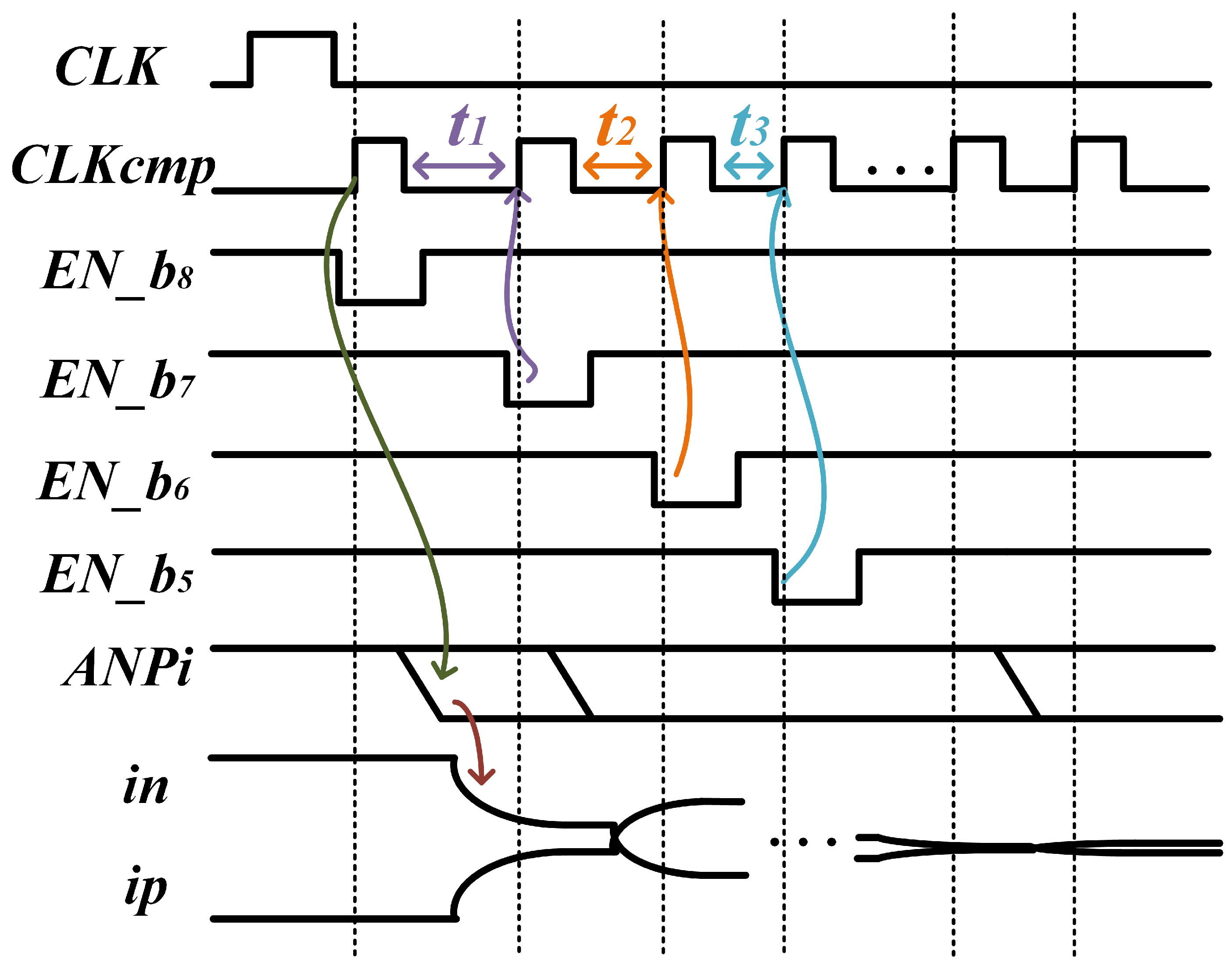
This paper provides a thorough analysis of the constraints that determine asynchronous time intervals during the conversion phase, and a brand-new delay adjustment logic for TBI is proposed, which serves as the basis for proposing an approach for high-speed SAR-ADC circuits.
2.
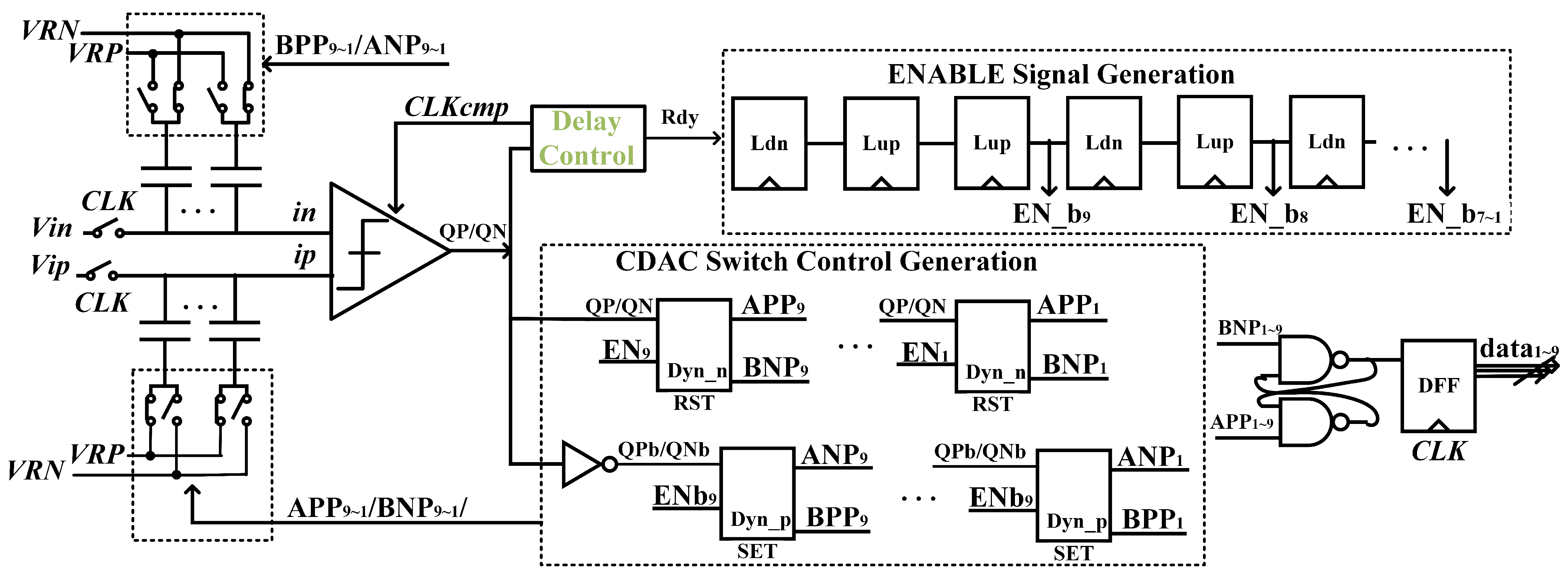
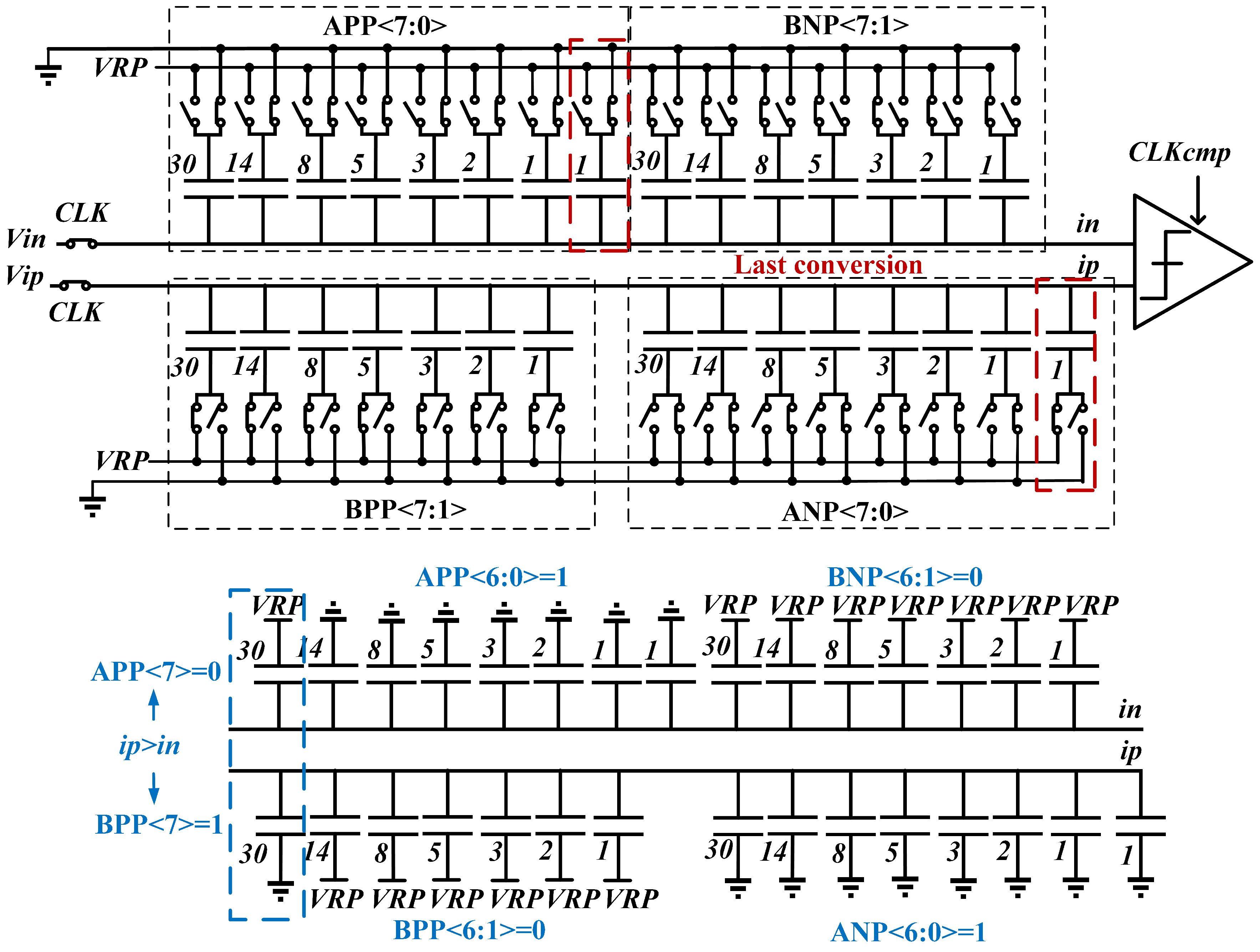
Based on the analysis, a high-speed SAR ADC is designed, presenting an 8-bit SAR ADC circuit implementation. Inverted dynamic latch pairs and early reset of capacitors are employed to improve speed. Split capacitive digital-to-analog converters (CDACs) by the latch pairs are employed to mitigate common-mode voltage shifts.
3.
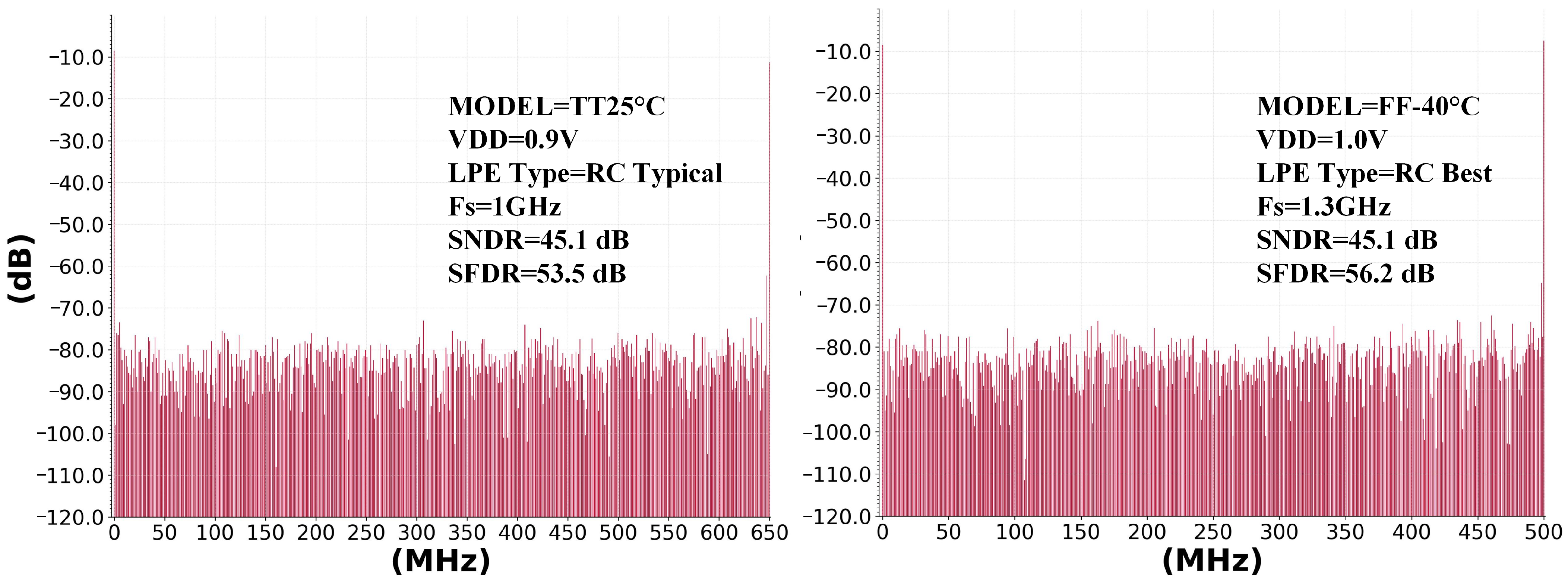
The post-layout simulation shows an effective number of bits (ENOB) of 7.20 bits at Typical–Typical (TT) 25 °C with a power consumption of 6.94 mW. With a sampling rate exceeding 1 GS/s across all process corners, our circuit also has the potential for application in high-speed multi-channel time-interleaved ADCs.
The paper is organized as follows: Section 2 introduces the theoretical foundation of the asynchronous clock cycle and derives the formula for the asynchronous clock period. Section 3 presents the design of the high-speed TBI-SAR-ADC circuit and describes each part of the circuit in detail. Section 4 showcases the simulation results. Finally, the conclusions are summarized in Section 5.

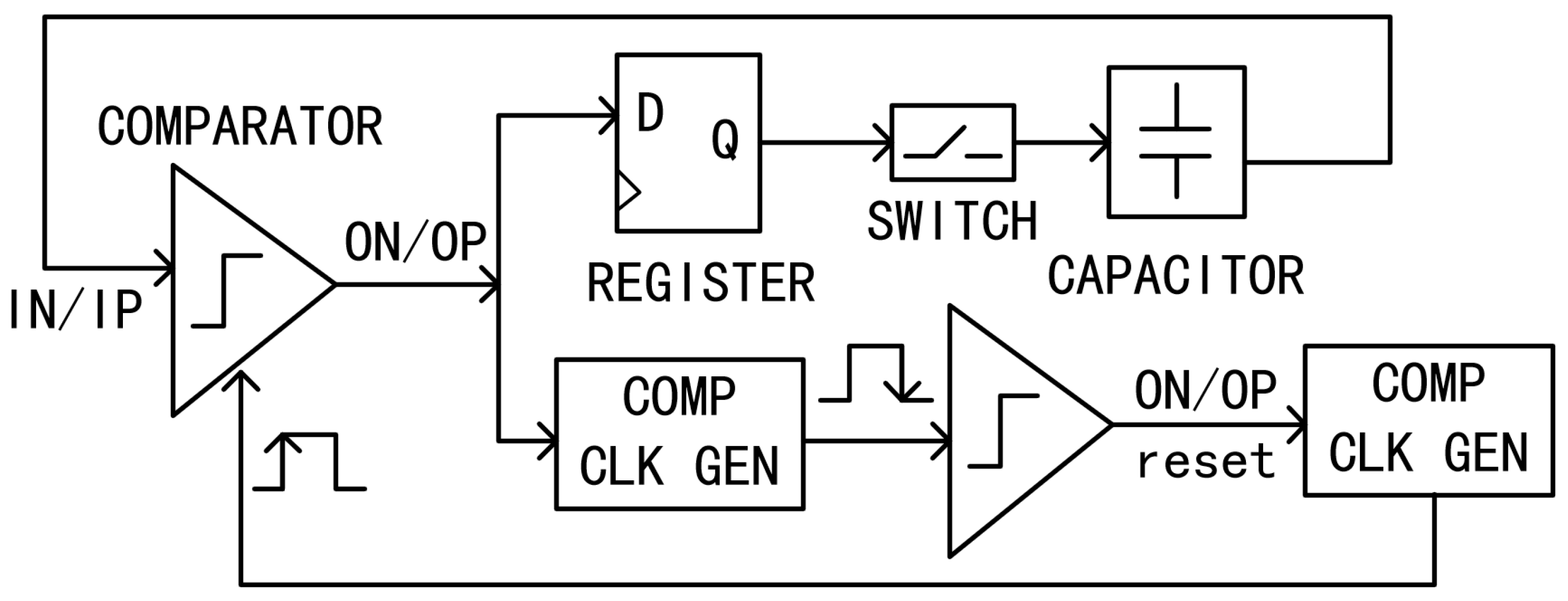
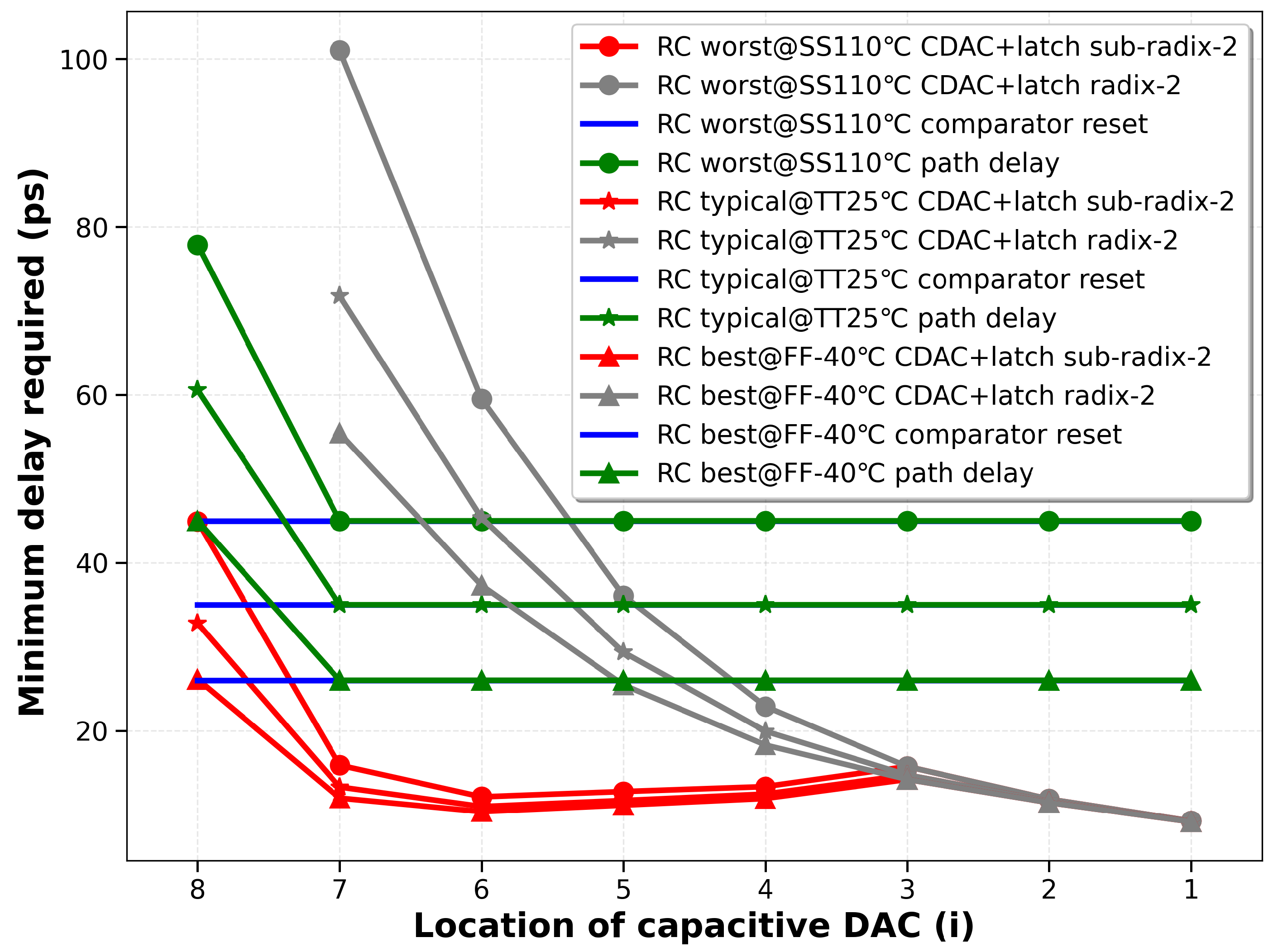
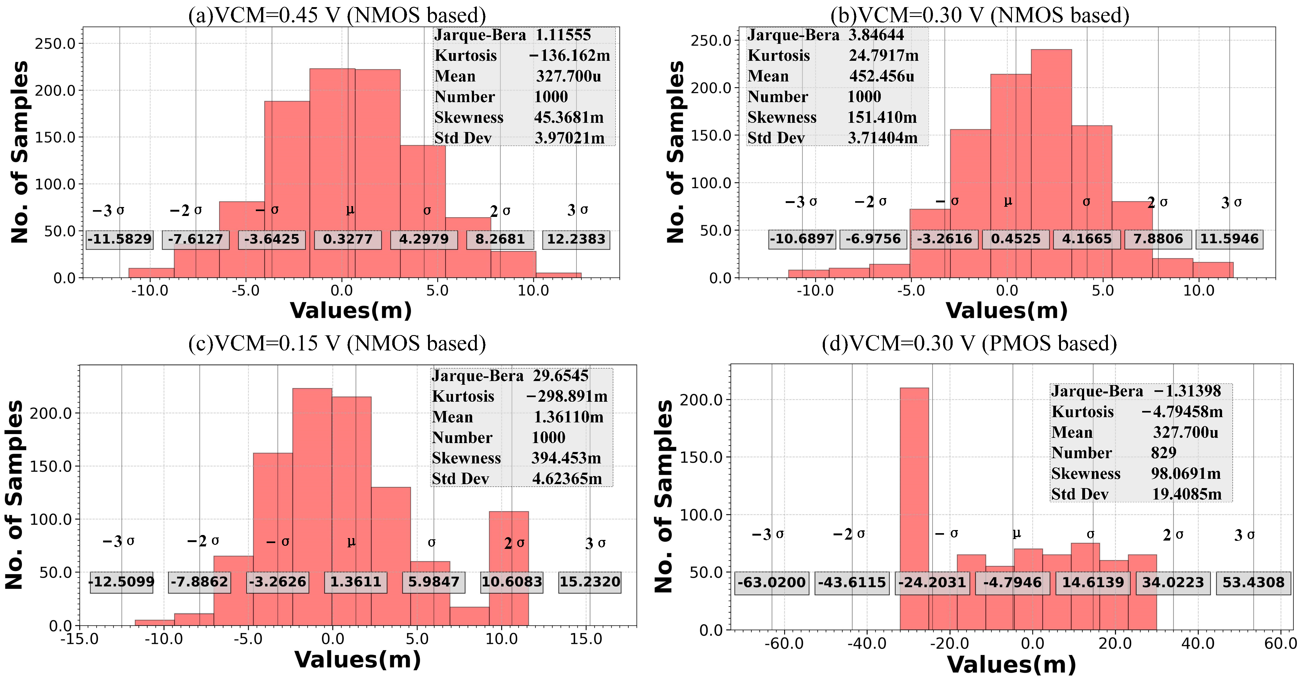
2. Analysis of CDAC Settling

Figure 1a illustrates the basic block diagram of an asynchronous SAR ADC, while Figure 1b shows the timing relationship between the asynchronous a s y _ C L K and external synchronous C L K during a single sampling and conversion cycle. During the high phase of C L K , the CDAC tracks the input signal. The falling edge of C L K triggers the asynchronous clock generation logic to produce a high-level voltage, initiating the first comparison. The asynchronous clock a s y _ C L K in the subsequent loops are generated based on the comparator output. After all bit decisions are completed, the asynchronous clock is reset to low.
Traditional SAR ADCs use the binary search algorithm to convert from the most significant bit (MSB) to the least significant bit (LSB) using comparators. During the conversion, the bottom plate of the capacitors is switched between the reference voltages based on the previous bit. The charge redistribution on the top plate of the capacitors then generates the input voltages for the next comparison. The timing relationships for each conversion are shown in Figure 2.
It can be seen that in the ideal case, the delay between two comparisons depends on the maximum of the CDAC path and the comparator reset path.
For the first m among n conversions, the following equation is satisfied:
t r e g i s t e r + t C D A C i > t l o g i c + t r s t _ c o m p ( 1 i m ) ,
where t r e g i s t e r denotes the input–output delay of the register storing the comparison result, t C D A C i denotes the i-th settling time of the CDAC, t l o g i c denotes the total delay of the comparator clock generation module, and t r s t _ c o m p denotes the comparator reset time. Supposing t l o g i c and t r s t _ c o m p are the same in every loop, we now derive the ideal minimum time of conversion from the following:
t c o n v e r s i o n = k = 1 n t c o m p k + k = 1 m t r e g i s t e r + k = 1 m t C D A C k + ( n m ) ( t l o g i c + t r s t _ c o m p ) ,
where t c o m p k denotes the time needed for the k-th comparison.
The duration of t C D A C i depends on the choice of capacitor weighting scheme. In the following, the CDAC settling time t C D A C i is derived for both binary-weighted (radix-2) and non-binary (with redundancy) schemes. In the conventional radix-2 scheme where the capacitors are binary weighted from MSB to LSB, the CDAC settling error needs to be within 1/2 LSB in each loop before the next comparison, to tolerate the effects of both comparator noise and other distortion. To attain accurate comparison results, the comparator has to be clocked right away or after when the DAC settles. This means that the clock generation module needs to add some delay to accommodate the DAC settling of the MSB. From this, we obtain a new expression for the conversion time after circuit implementation:
t c o n v e r s i o n = k = 1 n t c o m p k + n t r e g i s t e r + n t C D A C 1 ,
This means, for the lower conversion bits, there is unnecessary waiting time before the next comparison starts. For this reason, many studies have designed logic units with adjustable delays to approach the ideal conversion time in Equation (4). However, the adjustable delay unit usually extends the fixed delay in the comparator reset path for the complex logic, and increasing the precision of delay control also adds complexity to the control unit, making it more challenging to precisely control the delay of each loop [23,24].
In recent years, non-binary (sub-radix-2) capacitor circuits have been developed to allow us to clock slightly before the DAC settles. This approach not only relaxes the design requirements for delay logic but also tolerates more dynamic errors, such as insufficient DAC settling and comparator kickback. Below, we begin analyzing the delay under these two capacitor weighting schemes.
For an n-bit SAR ADC (whether using a binary or non-binary CDAC), in order to represent 2 n different values, the capacitance value C i for each conversion bit must satisfy the following condition:
C i k = 1 i 1 C k ,
where the right side of the inequality represents the sum of the capacitance values of the lower ( i 1 ) bits. For non-binary capacitor weights, the redundancy weight of the i-th conversion can be calculated using the following formula:
w r e d u n d a n t i = k = 1 i 1 w k w i ,
where the weight and the redundancy weight of the i-th conversion are denoted as w i and w r e d u n d a n t i . The i-th CDAC conversion requires sufficient time for the settling voltage to fall within the acceptable redundancy range so that the accuracy of the next comparison result is ensured as follows:
e t τ i w r e d u n d a n t i 2 n ,
where the time constant of the i-th conversion is denoted as τ i . If the capacitors are binary weighted, the RC-settling error voltage needs to be less than 1/2 LSB, and the CDAC settling time will be longer, as shown in the following:
e t τ i 1 2 2 n ,
Take the 8-bit ADC as an example: after adding one redundant bit, its weight radix is approximately 1.81. Since the process does not allow the selection of any non-integer multiple of the unit capacitance, we need to quantize the weights. Considering the symmetry of the layout, we choose even integers as the weights. In the top-plate sampling structure we use, the MSB is generated without DAC switching, and the first comparison is made directly with voltage on the top plate, so some redundant bits of the MSB are taken to the lower parts [26]. During the first conversion, the reference buffer requires a significant amount of current to charge the top plate of the DAC capacitors. As a result, more redundancy needs to be allocated to the second-bit weight to tolerate the potential unsettling error. According to the analysis above, the weights to be selected are (LSB): 120, 56, 32, 20, 12, 8, 4, 2, 1. Calculating the magnitude of the redundancy according to Equation (7), we obtain the corresponding redundant bits (LSB) as follows: 15, 23, 15, 7, 3, 0, 0, 0, 0.
Thermal noise is one of the main considerations when selecting the unit capacitance value C u . The following relation should be satisfied:
2 k T C s i n g l e , t o t a l ( V r e f 2 n ) 2 12 ,
where C s i n g l e , t o t a l means the single-ended sampling capacitance, and V r e f represents reference voltage. Ideally, if only the capacitance in the CDAC (with no parasitic capacitance) is considered, then C s i n g l e , t o t a l = 128 C u . Then, C u must be at least 0.1 fF to make ENOB at least 7.5 bits. Considering the process limit, non-ideal factors, and higher ENOB, the unit capacitor value is chosen as 0.732 fF.

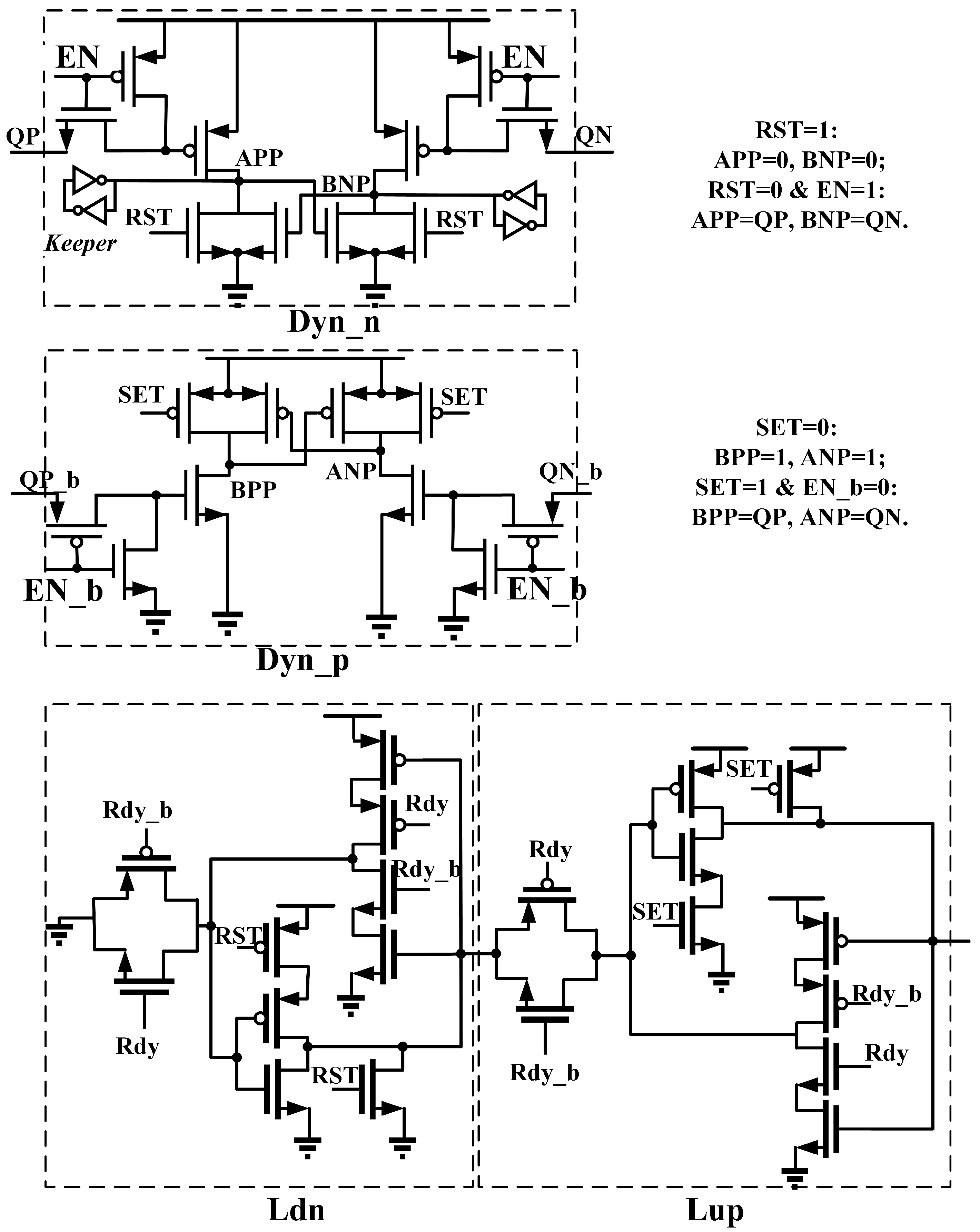
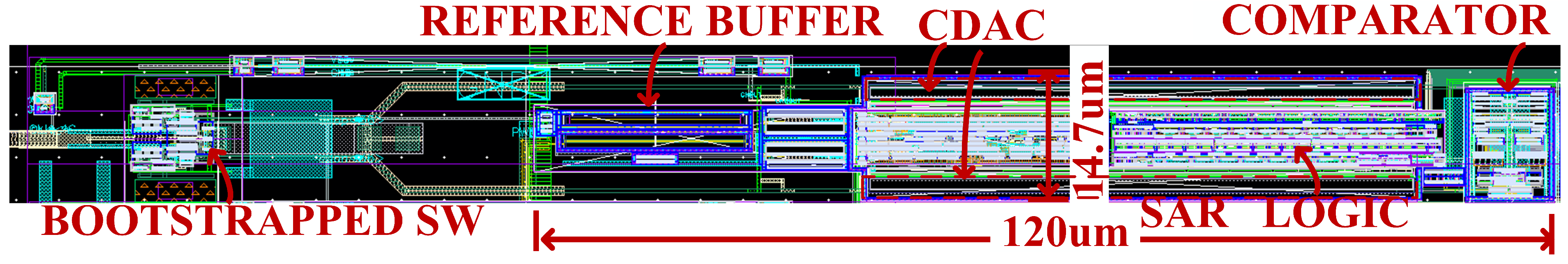
3. Circuit Implementation

As shown in Figure 3, the circuit uses the top-plate sampling technique, where the input voltage is directly sampled on the top plate of the capacitors, and eliminates the need for the CDAC switching before the first comparison. The conversion phase undergoes nine quantization steps, including one redundant bit, which ultimately reaches 8-bit precision. The timing diagram of the overall circuit can be seen in Figure 4. The bit weights are chosen as mentioned in Section 2.

3.1. Split Capacitors

Large common-mode variations at the comparator inputs may lead to dynamic errors, such as offset (the Monte Carlo simulations in Section 4 demonstrate the impact of common-mode voltage (VCM) shift on the comparator’s offset), which can impact accuracy. To mitigate this influence, split capacitors are used. The simultaneous conversion of the CDAC at both the i n and i p terminals ensures speed and maintains the common-mode voltage at the comparator input.
During tracking, the bottom plates of 64 unit capacitors at the i n terminal are connected to V R P (the voltage is 0.7 V), while 63 unit capacitors are connected to V R N (the voltage is 0 V), and the i p terminal is connected oppositely. After sampling, at the falling edge of the synchronous clock, the first comparison is triggered. After the comparator resolves its result, the switches corresponding to the capacitors are switched at the i n and i p terminals, as shown in the lower part of Figure 5.
In the final conversion, only the switches corresponding to the capacitors on one terminal (either i n or i p ) are switched. Since the voltage change during this final conversion is minimal, the resulting common-mode variation has a negligible impact on the comparator’s accuracy. This approach reduces the number of capacitors required by half compared to a conventional split capacitor method, which is particularly advantageous for multichannel interleaved ADCs with high bandwidth.

3.2. SAR Logic

In order to maintain a constant VCM, the differential terminals of the CDAC need to convert oppositely driven by the registers. Adding an inverter after the dynamic latch in [27] to drive the other differential output would increase the delay of the critical path. To address this, we propose a pair of inverted dynamic latches D y n _ n and D y n _ p , as shown in Figure 6. These latches, each driven by the enable clocks E N i and E N _ b i , can directly pass the comparison result to the CDAC switches within their active periods without the need to store the result. The enable clocks [26], requiring the R d y signal which is generated as shown in Figure 7, are activated half an asynchronous clock cycle before the comparator outputs. Therefore, when the comparator finishes resolving, the results are fed directly into the dynamic latch without waiting for a clock edge. Taking D y n _ n , for example, when E N i is low, the drain of the input NMOS is charged to V D D . When E N i is high, the voltage at the drain tracks the input voltage. There is only the input–output delay of the dynamic latch between the generation of the comparator’s result and the switches of the CDAC. The outputs of D y n _ n and D y n _ p are reset to 0 or 1, respectively, at the end of the last conversion, where an early reset is introduced in Section 3.4. The output of D y n _ n / D y n _ p is connected to a k e e p e r , a pair of back-to-back inverters. This is used to prevent charge leakage, which could otherwise lead to changes in the output voltage and subsequently affect the state of the switches.

3.3. Delay Generation Logic

From the analysis in Section 2, it can be concluded that the minimum delay between two consecutive comparisons depends on the maximum of the comparator reset path and the CDAC settling path. The latter is determined by the bit weight and the corresponding redundancy. Therefore, the delay for each loop may vary. Based on this, this work proposes a novel delay adjustment circuit that allows the tailoring of each bit interval.
The delay adjustment logic is easy to implement and does not introduce additional delay. As shown in Figure 7, it uses only three logic gates to generate the comparator clock. By controlling the number of PMOS transistors that are turned on, the current to VDD is controlled, thereby adjusting the delay for the transition from “0” to “1”. The circuit only increases the delay of the reset path without extending the “1” duration of the comparator clock. For example, when eight different reset path delays are required, eight sets of PMOS transistors are controlled by the eight enable clocks E N _ b 9 to E N _ b 2 , with each set containing a different number of PMOS transistors, resulting in varying delay lengths. In addition, the r s t signal is used to stop generating the comparator clock C L K c m p . The target tailored delay of each bit cycle, for example, t 1 , t 2 , t 3 , is shown in Figure 4. When the PMOS transistor size is smaller than 1 finger × 4 fins, it cannot sufficiently drive the subsequent circuit. When the size exceeds 12 fingers × 4 fins, the transistor’s intrinsic load becomes too large, preventing further delay reduction. The measured delay range in post-layout simulation is 20–38 ps under Fast-Fast (FF) at −40 °C, 31–45 ps under TT at 25 °C and 39–55 ps under Slow-Slow (SS) at 110 °C.

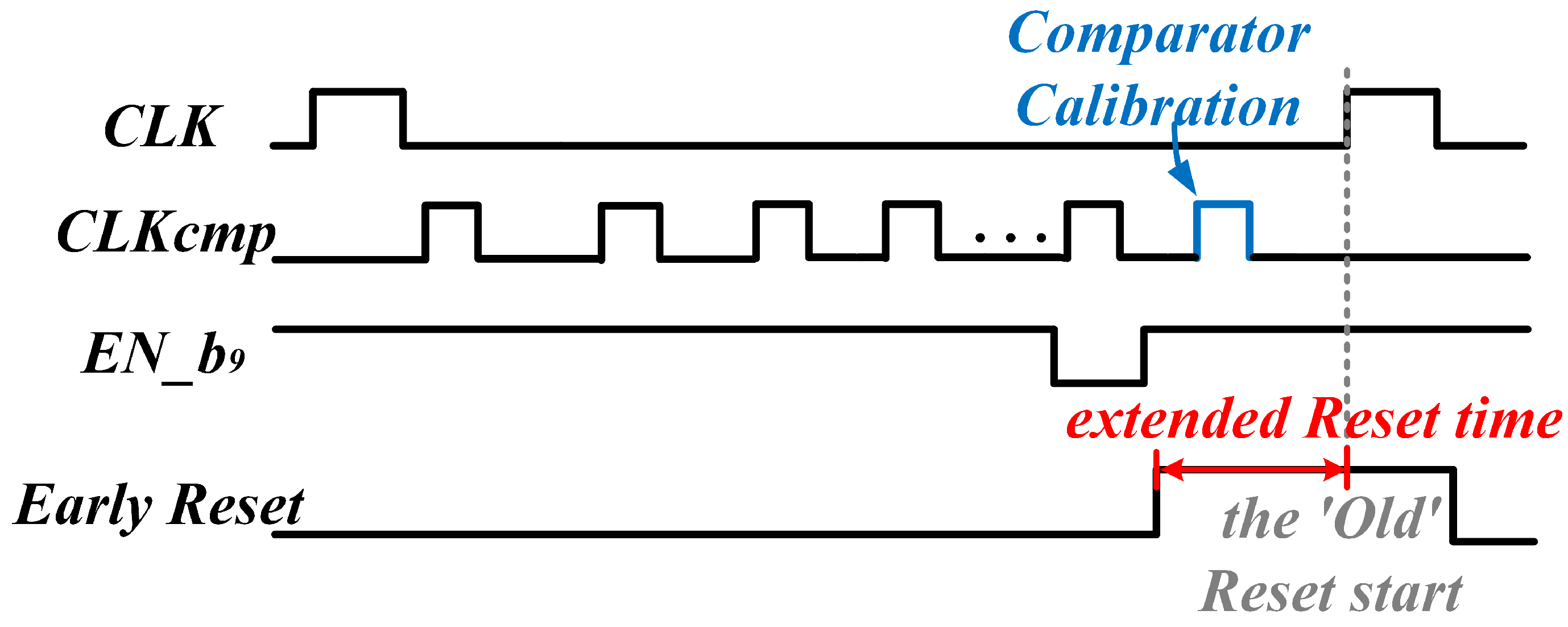
3.4. Early Reset of Dynamic Latch

Conventional ADC papers rarely mention the time consumed for resetting capacitor bottom plates. However, this is a critical consideration in high-speed ADC design. When the bottom plates of the capacitors are reset to the initial state, for example, with half connected to V R P and half connected to V S S in this implementation, a large current is required from the reference buffer. The limited driving capability restricts the reset speed, and it can take more than 100 ps. However, for multichannel interleaved ADCs with several stages of sampling, the final sampling switch may only be turned on for tens of picoseconds, which is not enough for the capacitors to reset. Thus, achieving an early reset is crucial; without it, a longer delay is needed before the next sampling period, and the maximum sampling rate may be limited, or the power consumption and area of the reference buffer could increase.
In this work, we propose a detection mechanism to early reset the capacitors, as shown in Figure 8. This mechanism allows for an early reset by detecting whether the ninth comparison is complete; otherwise, it will be reset by the external synchronized clock. During the capacitor reset process and before the next sampling, operations such as the comparator calibration can still be performed. Considering the limited driving capacity of the buffer, the ninth group of the latches, together with L u p s and L d n s, are synchronized with the external clock. Since their outputs no longer control the capacitor switching, the reset only needs to be finished before the next conversion starts.

4. Post-Simulation Results

Figure 9 shows the delays in the reset of the comparator, settling of the CDAC, and the comparator delay logic in three process corners, FF at −40 °C, TT at 25 °C, and SS at 110 °C. It illustrates the minimum delay required to satisfy Equations (8) and (9) for the CDAC settling time. As can be seen, the sub-radix-2 scheme effectively reduces the minimum time for the CDAC settling. In the delay logic design, it is crucial to ensure that during the first conversion, the path delay is greater than the CDAC settling time under the worst process corner. From the second loop, the reset time exceeds the CDAC settling time. Therefore, the path delay is determined by the comparator resetting time. Thus, two groups of delays are required in this ADC design ( t 1 > t 2 = t 3 ), as outlined in Section 3.3. The first PMOS group is controlled by E N 9 , and the second remains permanently open. This means that when a longer delay is needed, a portion of the PMOS transistors is turned off.
The TBI results in a 36.9% reduction in the total path delay compared to not using any delay adjustment. In addition, other more complex delay adjustment methods would increase the inherent delay of the reset path [23,24].
Figure 10 shows the Monte Carlo simulation results for the offset of the double-tail comparator, with 1000 points running at common-mode voltages of 0.15 V (NMOS-based), 0.3 V (NMOS-based), 0.45 V (NMOS-based), and 0.3 V (PMOS-based). It can be observed that during conversion when using the NMOS-based comparator, the VCM shift caused by monotonic conversion results in a higher probability of a large offset near the LSB (VCM = 0.15 V). Additionally, as VCM decreases, the comparator’s latency of sampling and propagation increases, which may increase the total conversion time. In contrast, when using a PMOS-based comparator, although the latency decreases with a reduction in VCM, the 3 σ offset increases significantly.
The proposed 8-bit SAR ADC with TBI is implemented in 16 nm FinFET technology. We use Virtuoso for initial design and simulation, Quantus for parasitic extraction. We use the 0.366 fF CSFMOM as a unit capacitor after splitting. Monte Carlo simulations in Virtuoso reveal a 3 σ mismatch of 2.85% for a single capacitor, resulting in a maximum INL of 0.455 LSB.
Figure 11 shows the layout of the proposed TBI-ADC, with the CDAC, the comparator, and the SAR logic, occupying only 0.0012 mm². The post-layout simulation results, including the highest sampling rates, effective number of bits (ENOB), across various temperatures and process corners, are presented in Table 1. Table 2 compares the post-layout performance of our TBI-ADC under TT and FF process corners with other silicon-proven state-of-the-art designs. In [20], to enhance the ADC speed, the SAR logic operates in parallel to the comparator, eliminating its timing from the critical loop by introducing a semi-asynchronous timing scheme. In [16], high-speed operation is achieved by converting each sample with two alternate comparators clocked asynchronously. In [28], multiple comparators are used to reduce the SAR loop delay, thus improving speed. In [29], a charge-injection SAR is introduced, and the ADC achieves GHz sampling speed and reduces area by more than half. The input signal frequency in our design is at the Nyquist frequency, and correlated sampling is employed. The output results are processed using a 1024-point FFT to obtain the ENOB. Notably, at the FF −40 °C and TT 25 °C corner, the highest sampling rate reaches 1.6 GS/s and 1.3 GS/s respectively, showing a 33% and 8.3% improvement over the fastest previously reported single-channel, 1 bit/cycle, 8-bit SAR ADC. Even under the SS process corner, this TBI-ADC exhibits competitive performance.
Figure 12 shows the post-layout 1024-point FFT simulation results for an input frequency at the TT 25 °C and FF −40 °C process corner. The post-layout simulated power consumption extracted at TT 25 °C RC typical is 6.94 mW, the CDAC consumes 5.34%, the logic 25.4%, and the comparator and its clock generation part 70%. If the efficiency and speed of the comparator are further optimized, the overall power consumption will improve significantly.

5. Conclusions

In this work, a thorough analysis of the delay in the CDAC settling of the asynchronous SAR ADC is given, and a novel TBI logic for high-speed ADCs is proposed. Inverted dynamic latch pairs and early reset of capacitors are employed to improve speed. A split CDAC is employed to mitigate common-mode voltage shifts. Simulated using the 16 nm process, the design demonstrates robust performance across various process corners. The post-simulation results show an ENOB of 7.20 bits at TT 25 °C and 7.21 bits at FF − 40 °C with a power consumption of 6.94 mW and 7.43 mW, respectively and a maximum sampling rate of 1.6 GS/s at FF −40 °C, demonstrating its potential for high-speed ADC applications. However, as technology scales, the conversion time becomes increasingly limited by the comparator reset time. Therefore, realizing a faster conversion loop with lower area overhead will be the focus of future research.

Author Contributions

Conceptualization, X.L.; methodology, X.L.; software, X.L. and R.W.; validation, X.L.; formal analysis, X.L.; investigation, X.L.; writing—original draft preparation, X.L.; writing—review and editing, X.L. and R.W.; visualization, X.L. and L.H.; supervision, K.Y. All authors have read and agreed to the published version of the manuscript.

Funding

This research received no external funding.

Data Availability Statement

All the data are reported/cited in the paper.

Conflicts of Interest

The authors declare no conflicts of interest.

References

  1. Luan, J.; Zheng, X.; Wu, D.; Zhang, Y.; Wu, L.; Zhou, L.; Wu, J.; Liu, X. A 56 GS/s 8 Bit Time-Interleaved ADC in 28 nm CMOS. Electronics 2022, 11, 688. [Google Scholar] [CrossRef]
  2. Wang, C.; Yang, Z.; Xing, X.; Duan, Q.; Zheng, X.; Gielen, G. A 10-Bit 400 MS/s Dual-Channel Time-Interleaved SAR ADC Based on Comparator Multiplexing. Electronics 2023, 12, 4062. [Google Scholar] [CrossRef]
  3. Cao, Y.; Zhang, M.; Zhu, Y.; Martins, R.P.; Chan, C.-H. A 12-GS/s 12-b 4× Time-Interleaved ADC Using Input-Independent Timing Skew Calibration with Global Dither Injection and Linearized Input Buffer. IEEE J. Solid-State Circuits 2024, 59, 4211–4224. [Google Scholar] [CrossRef]
  4. Tao, Y.; Gu, M.; Chi, B.; Zhong, Y.; Jie, L.; Sun, N. A 4.8GS/s 7-ENoB Time-Interleaved SAR ADC with Dither-Based Background Timing-Skew Calibration and Bit-Distribution-Based Background Ping-Pong Comparator Offset Calibration. In Proceedings of the IEEE International Solid-State Circuits Conference (ISSCC), San Francisco, CA, USA, 18–22 February 2024; pp. 394–396. [Google Scholar]
  5. Mittal, R.; Shibata, H.; Patil, S.; Krommenhoek, E.; Shrestha, P.; Manganaro, G.; Chandrakasan, A.P.; Lee, H.-S. A 6.4-GS/s 1-GHz BW Continuous-Time Pipelined ADC with Time-Interleaved Sub-ADC-DAC Achieving 61.7-dB SNDR in 16-nm FinFET. IEEE J. Solid-State Circuits 2024, 59, 1158–1170. [Google Scholar] [CrossRef]
  6. Gu, M.; Tao, Y.; He, X.; Zhong, Y.; Jie, L.; Sun, N. A 1-GS/s 11-b Time-Interleaved SAR ADC with Robust, Fast, and Accurate Autocorrelation-Based Background Timing-Skew Calibration. IEEE J. Solid-State Circuits 2025, 48, 421–431. [Google Scholar] [CrossRef]
  7. Ricci, L.; Bè, G.; Rocco, M.; Scaletti, L.; Zanoletti, G.; Bertulessi, L.; Lacaita, A.L.; Levantino, S.; Samori, C.; Bonfanti, A. A 2-GS/s Time-Interleaved ADC with Embedded Background Calibrations and a Novel Reference Buffer for Reduced Inter-Channel Crosstalk. IEEE J. Solid-State Circuits 2025, 60, 456–468. [Google Scholar] [CrossRef]
  8. Shiue, M.-T.; Lo, Y.-F.; Jung, C.-Y. Design of an Internal Asynchronous 11-Bit SAR ADC for Biomedical Wearable Application. Electronics 2024, 13, 3549. [Google Scholar] [CrossRef]
  9. Huang, Y.; Luo, C.; Guo, G. A Cryogenic 8-Bit 32 MS/s SAR ADC Operating down to 4.2 K. Electronics 2023, 12, 1420. [Google Scholar] [CrossRef]
  10. Tang, J.; Wang, Y.; Gu, H.; Zou, W. Design of Self-Calibration Comparator for 12-Bit SAR ADCs. Electronics 2023, 12, 2277. [Google Scholar] [CrossRef]
  11. Lakshmi, P.V.; Musala, S.; Srinivasulu, A.; Ravariu, C. Design of a 0.4 V, 8.43 ENOB, 5.29 nW, 2 kS/s SAR ADC for Implantable Devices. Electronics 2023, 12, 4691. [Google Scholar] [CrossRef]
  12. Yang, J.-I.; Yoon, K.S.; Lim, H. A 12-Bit SAR ADC with Binary Search Calibration Algorithm for a Split Capacitor. Electronics 2024, 13, 414. [Google Scholar] [CrossRef]
  13. Tang, H.; Xu, W.; Li, H.; Wei, B.; Wei, X. A 0.49–4.34 μW LC-SAR Hybrid ADC with a 10.85-Bit ENOB and 20 KS/s Bandwidth. Electronics 2024, 13, 1078. [Google Scholar] [CrossRef]
  14. Chan, C.H.; Zhang, M.; Cao, Y.; Zhao, H.; Martins, R.P.; Zhu, Y. The Race for the Extra Pico Second without Losing the Decibel: A Partial-Review of Single-Channel Energy-Efficient High-Speed Nyquist ADCs. In Proceedings of the IEEE Custom Integrated Circuits Conference (CICC), Denver, CO, USA, 21–24 April 2024; 2024; pp. 1–8. [Google Scholar]
  15. Li, X.; Wang, R.; Zhang, M.; Zhu, C.; Wang, Z.; Lin, J. A High-Speed 8-bit Single-Channel SAR ADC with Tailored Bit Intervals. In Proceedings of the IEEE International Symposium for Circuits and Systems (ISCAS), London, UK, 25–28 May 2025. [Google Scholar]
  16. Kull, L.; Toifl, T.; Schmatz, M.; Francese, P.A.; Menolfi, C.; Brändli, M.; Kossel, M.; Morf, T.; Andersen, T.M.; Leblebici, Y. A 3.1 mW 8b 1.2 GS/s Single-Channel Asynchronous SAR ADC with Alternate Comparators for Enhanced Speed in 32 nm Digital SOI CMOS. IEEE J. Solid-State Circuits 2013, 48, 3049–3058. [Google Scholar] [CrossRef]
  17. Kull, L.; Luu, D.; Menolfi, C.; Brändli, M.; Francese, P.A.; Morf, T.; Kossel, M.; Cevrero, A.; Ozkaya, I.; Toifl, T. A 24–72-GS/s 8-b Time-Interleaved SAR ADC with 2.0–3.3-pJ/Conversion and 30 dB SNDR at Nyquist in 14-nm CMOS FinFET. IEEE J. Solid-State Circuits 2018, 53, 3508–3516. [Google Scholar] [CrossRef]
  18. Jara, M.; Razavi, B. A 6-bit 10-GS/s 17.6-mW CMOS ADC with 0.8-V supply. In Proceedings of the IEEE Custom Integrated Circuits Conference (CICC), San Antonio, TX, USA, 23–26 April 2023; pp. 1–2. [Google Scholar]
  19. Tripathi, V.; Murmann, B. An 8-bit 450-MS/s single-bit/cycle SAR ADC in 65-nm CMOS. In Proceedings of the ESSCIRC (ESSCIRC), Bucharest, Romania, 16–20 September 2013; pp. 117–120. [Google Scholar]
  20. Ramkaj, A.T.; Strackx, M.; Steyaert, M.S.J.; Tavernier, F. A 1.25-GS/s 7-b SAR ADC with 36.4-dB SNDR at 5 GHz Using Switch-Bootstrapping, USPC DAC and Triple-Tail Comparator in 28-nm CMOS. IEEE J. Solid-State Circuits 2018, 53, 1889–1901. [Google Scholar] [CrossRef]
  21. Tsai, T.-H.; Tai, H.-Y.; Tsai, P.-Y.; Tsai, C.-H.; Chen, H.-S. An 8 b 700 MS/s 1 b/Cycle SAR ADC Using a Delay-Shift Technique. IEEE Trans. Circuits Syst. I Regul. Pap. 2016, 63, 683–692. [Google Scholar] [CrossRef]
  22. Qiu, L.; Tang, K.; Zheng, Y.; Siek, L.; Zhu, Y.; U, S.-P. A 16-mW 1-GS/s with 49.6-dB SNDR TI-SAR ADC for Software-Defined Radio in 65-nm CMOS. IEEE Trans. Large Scale Integr. (VLSI) Syst. 2018, 26, 572–583. [Google Scholar] [CrossRef]
  23. Gu, W.; Zhou, H.; Lin, T.; Wang, Z.; Ye, F.; Ren, J. Power efficient SAR ADC with optimized settling technique. In Proceedings of the IEEE International Midwest Symposium on Circuits and Systems (MWSCAS), Columbus, OH, USA, 2 December 2013; pp. 1156–1159. [Google Scholar]
  24. Kang, H.; Lee, S.; Lee, M. A Three-Step Tapered Bit Period SAR ADC Using Area-Efficient Clock Generation. Electronics 2023, 12, 1863. [Google Scholar] [CrossRef]
  25. Janke, D.; Monk, A.; Swindlehurst, E.; Layton, K.; Chiang, S.-H.; Wood, Y. A 9-Bit 10-MHz 28- μ W SAR ADC Using Tapered Bit Periods and a Partially Interdigitated DAC. IEEE Trans. Circuits Syst. II Express Briefs 2019, 66, 187–191. [Google Scholar] [CrossRef]
  26. Swindlehurst, E.; Jensen, H.; Petrie, A.; Song, Y.; Kuan, Y.-C.; Chang, M.-C.F.; Wu, J.-T.; Chiang, S.-H.W. An 8-bit 10-GHz 21-mW Time-Interleaved SAR ADC with Grouped DAC Capacitors and Dual-Path Bootstrapped Switch. IEEE Solid-State Circuits Letters 2019, 53, 83–86. [Google Scholar] [CrossRef]
  27. Huang, H.; Du, L.; Chiu, Y. A 1.2-GS/s 8-bit Two-Step SAR ADC in 65-nm CMOS with Passive Residue Transfer. IEEE J. Solid-State Circuits 2017, 52, 1551–1562. [Google Scholar] [CrossRef]
  28. Akkaya, A.; Celik, F.; Leblebici, Y. An 8-Bit 800 MS/s Loop-Unrolled SAR ADC with Common-Mode Adaptive Background Offset Calibration in 28 nm FDSOI. IEEE Trans. Circuits Syst. I Regul. Pap. 2021, 68, 2766–2774. [Google Scholar] [CrossRef]
  29. Choo, K.D.; Bell, J.; Flynn, M.P. Area-efficient 1GS/s 6b SAR ADC with charge-injection-cell-based DAC. In Proceedings of the IEEE International Solid-State Circuits Conference (ISSCC), San Francisco, CA, USA, 31 January–4 February 2016; pp. 460–461. [Google Scholar]
Figure 1. (a) Basic architecture of the asynchronous SAR ADC. (b) Timing relationship between external clock and asynchronous clock.
Electronics 14 02032 g001
Figure 2. The timing relationship between the CDAC settling path and the comparator reset path in a SAR ADC loop.
Electronics 14 02032 g002
Figure 3. The overall diagram of the high-speed 8-bit SAR ADC.
Electronics 14 02032 g003
Figure 4. The timing diagram of the signals.
Electronics 14 02032 g004
Figure 5. The overall architecture of the split capacitor circuit (top) and the diagram showing the initial and first switch of the capacitor (bottom).
Electronics 14 02032 g005
Figure 6. The circuit of the dynamic latch.
Electronics 14 02032 g006
Figure 7. The circuit of the delay adjustment for the TBI-SAR-ADC.
Electronics 14 02032 g007
Figure 8. The timing diagram shows that the early reset mechanism extends the reset time.
Electronics 14 02032 g008
Figure 9. Post-layout results showing the delays in the comparator reset, the CDAC settling (minimum), and the comparator delay logic in different corners.
Electronics 14 02032 g009
Figure 10. 1000-point Monte Carlo simulation results of the comparator offset with different VCMs.
Electronics 14 02032 g010
Figure 11. Layout of the high-speed 8-bit SAR ADC.
Electronics 14 02032 g011
Figure 12. 1024-point FFT of the post-simulation result at TT 25 °C and FF−40 °C and Nyquist input frequency.
Electronics 14 02032 g012
Table 1. TBI-SAR-ADC performance of post-layout simulation at different corners.
ModelLPE TypeVDD = 0.9VTemp.Max. S. R.ENOB
TTRCtypicalnominal25 °C1.3 GS/s7.20@1 GS/s
FFRCbest1 + 10%−40 °C1.6 GS/s7.21@1.3 GS/s
FFRCbest1 + 10%110 °C1.4 GS/s7.18@1 GS/s
SSRCworst1 − 10%−40 °C1.05 GS/s7.05@0.9 GS/s
SSRCworst1 − 10%110 °C1 GS/s7.08@0.8 GS/s
Table 2. Performance comparison between this work (post-layout simulation) and state-of-the-art silicon-proven SAR ADCs.
JSSC [20]JSSC [16]TCAS1 [28]ISSCC [29]This Work
Technology28 nm32 nm SOI28 nm FDSOI40 nm16 nm FinFET
ADC TypeSAR2-compSARLU-SARci-SARSAR
Supply [V]1.01.01.01.01.0        0.9
f s [GS/s]11.20.811.6       1.3 (max)
Resolution [bit]78868
SFDR [dB]52.049.850.749.756.2      53.5    @1.3 & 1 GS/s
SNDR [dB]40.139.342.634.645.1      45.1    @1.3 & 1 GS/s
FOMw [fJ/conv.-s]34.43422.828.726.0      24.3    @1.3 & 1 GS/s
Disclaimer/Publisher’s Note: The statements, opinions and data contained in all publications are solely those of the individual author(s) and contributor(s) and not of MDPI and/or the editor(s). MDPI and/or the editor(s) disclaim responsibility for any injury to people or property resulting from any ideas, methods, instructions or products referred to in the content.

