Abstract
For the past few decades, metal–oxide–semiconductor field-effect transistors (MOSFETs) have been the most important application in IC circuits. In certain circuit applications, the breakdown voltage and specific on-resistance serve as key electrical parameters. This article introduces a readily accessible approach to enhance the source–drain breakdown voltage (BVDS) of MOSFETs based on the Bipolar-CMOS-DMOS (BCD) platform without extra costs. By attentively refining the process steps and intricacies of the doping procedures, the breakdown voltages of NMOS and PMOS experienced increments of 3.4 V and 4.6 V, translating to enhancements of 31.5% and 50.3%. Parallel simulations offer insightful mechanistic explanations through simulation tools, facilitating superior outcomes. This initiative lays significant groundwork for the advancement of a comprehensive BCD process development framework.
1. Introduction
Semiconductor power devices find extensive applications across various domains including power control, automotive electronics, consumer electronics, and communication electronics [1]. The inherent benefits of these power devices encompass rapid switching speed, convenient driving mechanisms, and the absence of secondary breakdown voltage [2,3]. Metal–oxide–semiconductor field-effect transistors (MOSFETs) as the core part of logic control have several important functions in power device systems. In the area of MOSFET optimization, the prime objectives remain the augmentation of circuit power conversion efficiency while concurrently mitigating the overall expenditure of the product. Breakdown voltage drain to source (BVDS) and specific on-resistance (Ron,sp) are consistently acknowledged as pivotal operational metrics for transistors, serving as quintessential performance benchmarks for power MOSFETs [4].
BVDS is when the voltage between the source and drain reaches a critical value, causing the device breakdown. There are three mechanisms of breakdown for a MOSFET besides the breakdown caused by defects in the gate oxide itself, as illustrated in Figure 1. Drain–source breakdown (Figure 1a) is when the reverse bias voltage is applied to the drain; the depletion region of the drain/bulk PN junction is extended. When the depletion region touches the source, a path is formed between the source and the drain without opening, so it is called punch-through [5]. To prevent this, an “anti-punch-through” step is included in the process, which involves increasing the doping concentration to limit the width of the depletion region. The breakdown between the drain and bulk, known as avalanche breakdown, occurs when a reverse bias voltage is applied to the drain, causing the depletion region of the PN junction to widen. The reverse-bias electric field, along with the reverse bias of the PN junction, accelerates electrons, leading to collisions with the crystal lattice and the generation of new electron–hole pairs. This cascade effect of electron collisions triggers a breakdown, as depicted in Figure 1b. Therefore, it is crucial to consider the doping profile to prevent this junction breakdown carefully. Another breakdown mechanism is drain–gate overlap oxide breakdown (Figure 1c), which is similar to the gate oxide breakdown of the poly finger. To avoid this type of breakdown, special attention should be paid to the poly profile and sidewall. Additionally, the breakdown can also be triggered by the phenomenon of GIDL (gate-induced drain leakage). Understanding the breakdown mechanisms of MOSFETs is essential for effectively adjusting the doping concentration of the PN junction and improving BVDS [6,7,8]. Specific on-resistance refers to the ratio of drain current to voltage when a certain voltage is applied between the drain and source of a MOSFET. Generally speaking, the breakdown voltage is influenced by several factors, including the thickness of the gate oxide layer, the separation between the drain and source, and the doping concentration [9,10,11]. BVDS and Ron,sp are two key parameters, which are affected by factors such as the device structure and material and the process of the transistor.
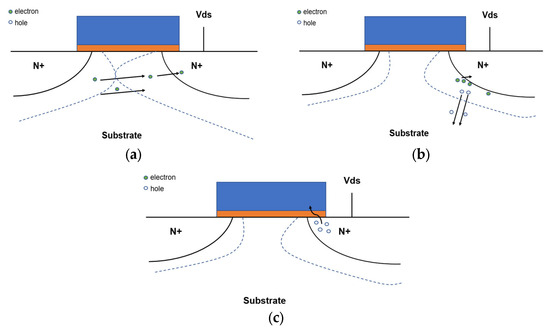
Figure 1.
Three breakdown mechanisms of MOSFET: (a) drain–source punch-through breakdown; (b) drain–bulk junction breakdown; (c) drain–gate overlap oxide breakdown.
Normally, the minimum breakdown voltage designated for MOSFETs employed in logic switching and bias modulation is strategically set at approximately twice the operational voltage, with NMOS devices slightly surpassing the breakdown voltage of PMOS [12]. Additionally, high-end driving MOSFETs typically need a gate voltage higher than the source voltage during operation [13]. Upon activation of the high-side driven MOSFET, where the source voltage aligns with the drain voltage (VCC), the gate voltage exceeds VCC. However, if a voltage exceeding VCC is sought within the same system, the implementation of a dedicated boost circuit becomes imperative [14]. A heightened source–drain breakdown voltage not only fortifies the voltage endurance of the transistor but also amplifies output power and efficacy in elevated-voltage scenarios. Moreover, it plays a critical role in mitigating transistor losses during operation, thereby prolonging its operational lifespan and reducing overall expenses [15,16,17]. Thus, the thorough optimization of the source–drain breakdown voltage (BVDS) attributes of MOSFETs and the delicate equilibrium between BVDS and Ron,sp bear immense significance in elevating the performance of power devices. The unique specifications of this project dictate that the operating voltage must be elevated to around 7 V. Consequently, the designated target breakdown voltages for this project are established at 14 V for NMOS and 13 V for PMOS. This innovative design enables the device presented in this project to offer an expanded voltage dynamic range without adding additional parts to the circuit, thereby enhancing linearity. Simultaneously, it facilitates an increase in switching speed and minimizes losses during the switching process, rendering it well suited for prospective high-frequency applications [18].
Beyond considerations of structural design, material composition, and the quality of oxide layers, doping concentration emerges as an indispensable variable in the manufacturing methodology, particularly due to its keen impact on the breakdown voltage [19]. Through meticulous adjustment of procedures and optimization of the intricate parameters within the CMOS process, with particular emphasis on the ion implantation phase, the source–drain breakdown characteristics of MOSFET devices can be notably enhanced. Plenty of studies has been reported previously; however, the majority have focused on increasing the BVDS of the device through the innovation of structural designs such as adding extra field plates or insulator layers or changing and adding new materials [20,21,22]. The introduction of the new structure will undoubtedly elevate the challenges associated with process manufacturing and amplify the complexity of the circuit. Meanwhile, the incorporation of novel materials may present significant compatibility issues with CMOS during fabrication and application processes. However, in industrial production, the most accepted and widely used way to improve the electrical properties of devices is to change the process conditions without incurring additional costs.
This article demonstrates a method to improve the device performance without extra cost simply by adjusting the process sequence and changing the process conditions. This article starts from the design requirements and subsequently refines the fundamental process steps. Utilizing the Sprocess simulation tool from TCAD Sentaurus, it analyzes the ramifications of device alterations stemming from process modifications. Furthermore, the Sdevice module is employed to assess the electrical parameters of the devices. The parameters derived from the simulation serve as a benchmark for real process optimization during tape-out. By continuously refining the process parameters, the properties of the 7 V MOSFET were progressively enhanced, ultimately culminating in the fulfillment of the design targets.
2. Basic Mechanism and Manufacturing Process
The foundational process is rooted in the standardized 55 nm CMOS process, laying the groundwork for progressing toward logic and high-voltage MOSFET devices within the purview of BCD process development. Generally, increasing the operating voltage of the logic control unit can indeed provide a wider input signal range, thus enhancing the flexibility and applicability of the system [23]. Moreover, the increased voltage can enhance the driving capability of the unit, allowing it to drive more loads or more complex circuits, enabling the system to achieve more intricate functions or improve its operating speed [24,25,26]. Additionally, the increase in operating voltage can positively impact aspects such as response time, power consumption, and performance in special application scenarios [27,28,29]. Hence, in alignment with the design requirements, the 5 V logic MOSFET in this project needs to drive up to 7 V while maintaining the original size and structure; consequently, the breakdown voltage must also be increased. Given the distinct design requirements and device traits, a strategic choice was made to enhance the performance of both NMOS and PMOS through individual process optimization endeavors. The basic process flow of BCD is shown in Figure 2. The main process adjustments focus on the three parts including the well module, lightly doped drain (LDD) module and source–drain module, indicated by the solid red line as illustrated in Figure 2, which significantly influence the device performance. In this project, a dual-well process is employed, where the ion implantation process is carried out separately for NMOS and PMOS, each with distinct parameters.
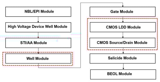
Figure 2.
Basic key process flow chart.
2.1. Well Module
In the process flow, given that precise ion implantation plays a pivotal role in influencing the electrical properties and alleviating problems such as ‘latch-up effect’, the dual-well process typically entails a segmented approach, conducted in several steps [30]. In detail, in the well process, the ion implantation of the well module includes three steps for well N. (1) Phosphorus ions are implanted at a greater depth and higher energy to adjust the well concentration, reduce well resistance, and prevent latch-up effects (well implantation). (2) Phosphorus ions with a smaller depth and lower energy are injected to adjust the channel concentration and increase the concentration of the well below the LDD area, making the depletion layer at this location narrower when the device is operating, preventing source–drain penetration leakage of the device (anti-punch-through, APT). (3) Arsenic ions are implanted on the surface with lower energy to adjust the PMOS threshold voltage Vt (Vt adjustment).
For well P, the process method of ion implantation is similar, except that phosphorus and arsenic ions are replaced by boron and BF2, respectively. The wells are then annealed to repair the lattice damage, which is also a critical step for the well formation. High-temperature furnace annealing is employed to activate the impurity ions within well N and well P, as well as to rectify lattice damage, while ensuring that the doped ions are positioned at the designated depth [31,32].
2.2. LDD Module
As for the LDD module, two steps of LDD ion implantation are required. (1) Arsenic ion implantation is performed with a shallower implant depth to establish a low-doping extension region beneath the gate boundary and situated between the source and drain; this extension area creates a gradient in impurity concentration between the source, drain and channel. This modification serves to lower the peak of the lateral electric field near the drain, thereby enhancing the device’s overall device reliability and avoiding the hot carrier injection (HCI) effect. (2) Boron ion implantation is then performed, with a deeper implant depth and higher energy which is used as “pocket” implantation. Utilizing “pocket” implantation within LDD structure enhances the doping concentration at the interface between the substrate and the source and drain regions. This approach reduces the width of the source and drain depletion regions, effectively suppressing the drain-induced barrier-lowering (DIBL) effect in short-channel devices. In addition, the type of “pocket” ion implantation matches that of the substrate; for instance, NMOS devices use p-type implantation, while PMOS devices employ n-type implantation. BF2 and phosphorus are implanted, respectively, in the PLDD process, and the dose and energy are similar to NLDD. There is usually a spacer process between the LDD and source–drain modules. Spacers can protect the LDD structure, and the width and height of the spacer can also affect the device’s performance.
2.3. Source–Drain Module
Low energy, shallow depth and heavily doped ion implants are widely used in source–drain implantation modules. Arsenic and phosphorus ions are implanted to form the source and drain of heavily doped NMOS, and PMOS is implanted with BF2. After removing the photoresist, annealing and activation are conducted separately for the device. It should be noted that, due to the dual-well process being used, the generation of NMOS and PMOS necessitates the completion of their respective modules before proceeding to the next module.
Based on the basic process described above, we aim to enhance the performance of the MOSFET device in this experiment by adjusting the sequence of steps and certain parameters.
3. Process Adjustments and Discussion
3.1. Mechanism Analysis and Process Adjustments
Diverse process optimization modifications have been executed for the 7 V N-type and P-type MOSFET devices in the three modules mentioned above. These adjustments more or less improve the breakdown and resistance characteristics of the device. Improvements in doping profiles, ground rules, and device layouts were optimized simultaneously for device performance through the assistance of the predictive TCAD simulation [33]. A proper simulation model was set. The avalanche breakdown model was introduced to describe the breakdown behavior of source–drain punch-through under high-electric-field conditions for MOSFETs. In addition, a drift-diffusion model was used to simulate the drift and diffusion behavior of the carriers in the electric field. The simulations were processed using adaptive mesh refinement, and the drain voltage was capped at 15 V and the temperature was 25 °C.
The mechanism explanation here takes NMOS as the example. The MOSFETs work because when a reverse bias voltage is applied to the drain, the depletion region of the PN junction extends. Once the depletion region reaches the source, a path is formed without the need for the source and drain to be open. Hence, preventing punch-through and avoiding the increase in p-type dose concentration become crucial. This reduces the P-well concentration and increases the N-well concentration, which helps to increase the depletion region width and reduce electric field concentration effect of the P-N junction, thereby increasing the breakdown voltage of the device and improving the device’s capability to withstand voltage, as shown in Formula (1), where BV represents the source–drain breakdown voltage, is the dielectric constant of silicon, is the element charge, Na is the impurity concentration of the P-type region, and Wdep is the depletion region width [34].
Given the preceding information, we have enacted the subsequent refinements: canceling/skipping the ion implantation dosage for well P and concomitantly amplifying the ion implantation dosage for well N. Concerning well P, the photoresist remains uncovered, facilitating the ion implantation process for well P in tandem with the ion implantation for well N. In essence, the ion implantation for both NMOS and PMOS is executed during the pivotal ‘channel stop’ phase. Subsequently, following the previous step, one should reduce or skip the APT ion implantation of well P to increase the ion dose in of well N in NMOS, and adjust the APT and Vt adjustment steps of well P to increase the ion dose in PMOS.
By modifying the doping specifics at this step, it is apparent that the extent of the depletion region experiences a notable rise, illustrated by the white line in Figure 3. Furthermore, the breakdown width of the PN junction undergoes a remarkable expansion, rendering the device more resilient to breakdown and consequently enhancing its breakdown tolerance performance, as depicted from Figure 3a,b. By skipping or decreasing IMP-APT (implantation of anti-punch-through), the dose of PW-IMP can be significantly reduced, which has been confirmed in actual tape-out, thereby enhancing the BVDS of NMOS from 12.15 V to 14 V (skipping IMP-APT 2 in the process flow).
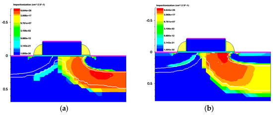
Figure 3.
Skipping IMP-APT to improve BVDS of NMOS. (a) NMOS fabricated according to the original process; (b) NMOS with the IMP-APT step skipped and other steps remaining unchanged.
In Figure 4, by reducing the energy level of well P and increasing the concentration of boron in the channel area, it becomes more difficult to meet the breakdown point. This is evident when comparing the doping concentration. After this step, additional adjustments to the dose and energy of APT-IMP were made, along with threshold voltage (Vt). Following the previous step, the BVDS of PMOS was raised to 14.5 V, significantly surpassing the target voltage.
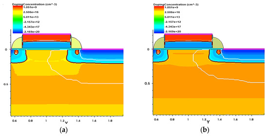
Figure 4.
PMOS (a) before and (b) after the reduced ion implantation dose simulated by TCAD.
For the LDD module, NLDD remains unchanged; the steps of PLDD and PLDD-RTA (Rapid Thermal Annealing) are skipped (or reduced). PLDD and PLDD-RTA are moved to the P-type step source drain implantation, which does not require the extra photomask for PLDD. It is feasible to perform PLDD simultaneously with source and drain implantation. This may help achieve a more uniform doping profile, and by combining the steps, defects and stress caused by multiple processes can be reduced, thereby improving the overall reliability of the device. However, this requires more precise control of doping concentrations overall to guarantee that the doping levels in both the source–drain and channel regions align with the design specifications. Furthermore, greater precision is essential during the thermal annealing process to ensure the effective activation and diffusion of the doping ions, which means that the need for thermal treatment must be carefully balanced.
In the 55 nm CMOS flow for PMOS, the synergy of skipping PLDD and PLDD-RTA while performing the extra pocket implantation (PKT-IMP) leads to a noteworthy improvement from 10.85 V to 12.6 V.; the simulation results are shown in Figure 5. Nonetheless, this approach also carries certain adverse repercussions, notably a substantial spike in the device’s leakage current as indicated in Table 1 (rising from 0.102 pA/um to 1.11 pA/um). Skipping the inversion LDD structure increases electric field bending near the drain area, leading to a higher leakage current, harming device switching speed, and raising driving power consumption.
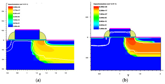
Figure 5.
Without (a) and with extra (b) PLDD and PKT-IMP after spacer deposition in PMOS.

Table 1.
Electrical test results of different devices before and after process adjustment.
Regarding the source–drain module, upon completion of the spacer deposition, one should proceed with pocket implantation of PLDD and PLDD implantation for PMOS (together with PMOS source drain implantation). In a better NMOS condition, further optimization is performed to skip the P-well photo, and one should skip well P or increase the ion implantation dose of well N to effectively reduce Isoff (subthreshold leakage current) and improve BVDS. Similarly, in an enhanced PMOS setting, decreasing the N-well and P-well APT dose can elevate the BVDS of PMOS.
Additionally, based on the superior NMOS BVDS data previously acquired, the value can be further improved by optimizing the source and drain doping process. By skipping NP-IMP3 (the third step of source/drain implantation) and intensifying the N-well implantation dosage, the Isoff is reduced, leading to an increase in BV. As illustrated in Figure 6, in comparison with Figure 6a, the depletion region’s depth near the drain area of Figure 6b is enlarged, with more extensions reaching the source zone. The white depletion-region line in the channel is lower, indicating that this region is more difficult to penetrate. It can decrease the leakage current of the PN junction and lower the leakage current level in the off-state of the device. Carrier distribution and migration in the channel can be impacted and the depletion region at the channel is widened, thereby enhancing the transistor’s conduction characteristics and boosting switching speed and output characteristics. These findings are further supported by practical data. The BVDS of NMOS has been elevated to 14.2 V and shows potential for further enhancement. The ultimate performance metrics of both NMOS and PMOS are detailed in Table 1 (which is the final result for this stage).
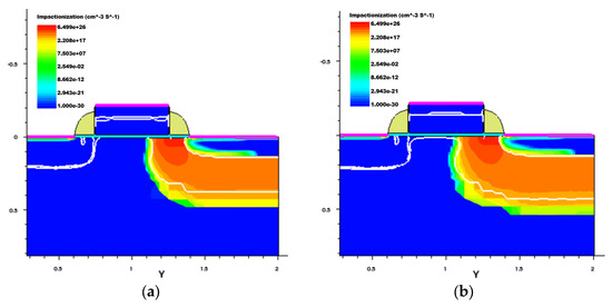
Figure 6.
(a) Before and (b) after optimization of the source-drain ion implantation process to improve BVDS of NMOS.
Through various experiments conducted on wafers from multiple batches, we have been able to observe the enhancement in the BVDS process of NMOS and PMOS, as illustrated in Figure 8. It is evident that for NMOS, the most notable impact is witnessed when certain APT-IMP process steps are either omitted or reduced (from wafer 4 to wafer 5). On the other hand, significant performance improvements in PMOS have been consistently achieved by skipping the PLDD-IMP, PLDD-RTA, and PW-PH steps, while incorporating pocket-IMP and PLDD-IMP after spacer deposition. These findings align with the outcomes derived from simulations.
3.2. Results and Electrical Test
As illustrated in Figure 7, the wafer after process adjustment is sliced, and the 7 V n-type NMOS device is selected for further analysis. As the device operating voltage increases from 5 V to 7 V, the gate oxide thickness increases from 120 Å to 170 Å to better prevent oxide breakdown and leakage. A wafer acceptance voltage (WAT) test was also conducted. The test condition of BVDS involves a drain sweep voltage range of 0–15 V at a step of 0.05 V until the IDS larger than 0.1 μA/μm*W. Specific on-resistance cannot be measured directly, calculated as VDS divided by IDS [35,36]. Based on the above work, we also evaluated other aspects of device performance to fully understand the improvement of device performance, as shown in Table 1, and the test results in the table have met the design requirements in the device design rules.
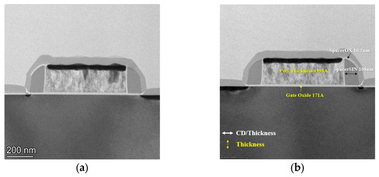
Figure 7.
Cross-sectional TEM image: (a) the selected position of the fabricated wafer; (b) the final device of NMOS.
As shown in Figure 8, with the improvement of the process, the breakdown voltage of NMOS and PMOS has been improved to a certain extent. The notable enhancement of NMOS performance from wafer 4 to wafer 5 can be attributed to the optimization of the APT-IMP step, while the BVDS improvement of PMOS arises from the synergistic impact of the above three stages mentioned in part II, with particular emphasis on the source and drain ion implantation stage.
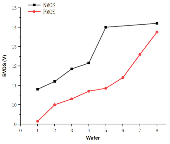
Figure 8.
The trend of process improvement of breakdown voltage for NMOS and PMOS.
A comparative analysis was carried out on the performance curve (illustrating Ron,sp versus BVDS) of the 55 nm platform device in relation to other devices of similar types but operating at varying voltages and nodes [37]. The results are shown in Figure 9. The horizontal x-axis of the graph represents BVDS, while the vertical y-axis signifies the Ron,sp. The solid data points correspond to N-type MOS devices, while the hollow data points represent P-type devices. The differentiation in colors and shapes denotes devices from disparate platforms and nodes. As shown in Formula (2), the figure of merit (FOM) value of the device is an important reference for measuring the quality of electrical indicators [38]. The FOM values of NMOS and PMOS calculated in this experiment are 32.0 V2/(mohm*mm2) and 85.9 V2/(mohm*mm2) respectively, which are significantly better than the reports and initial results in other studies.
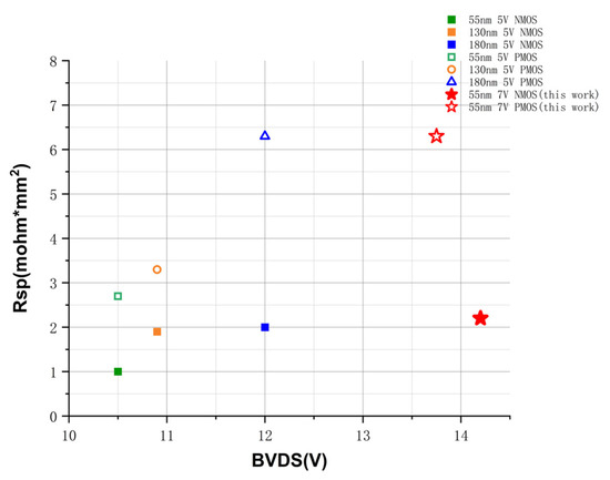
Figure 9.
Comparison of performance among the devices described in this work and other work reported in the literature.
Despite the differences in node sizes and operational voltages among these devices, those within this particular project consistently demonstrate superior performance characteristics, exhibiting lower Ron,sp values and higher BVDS. The optimization of the MOSFET process is also applicable to other components in the BCD platform. These components include low-voltage CMOS devices with analog compatibility, BJTs, resistors of 0.3 to 40 k Ω/square, 5–60 V capacitors, Schottky diodes, Zener diodes and double-layered metals [39].
4. Conclusions and Limitations
This article emphasizes the process optimization and improved electrical performance of MOSFET devices with varied doping profiles. The presented method offers the highest reported BVDS of a standard 7 V MOSFET for both NMOS and PMOS. Simulation outcomes aptly demonstrate the optimization of these parameters in relation to device performance, particularly accentuating the source–drain breakdown voltage. The experimental outcomings corroborate the simulations, showcasing notable BVDS upgrades of 3.4 V for NMOS and 4.6 V for PMOS, translating to enhancements of 31.5% and 50.3%, respectively. This result has also been verified by multiple tape-outs as a stable and effective result, which is an improvement for the standard fabricated process that can be widely used for MOSFETs. The optimization of the MOSFET process is also applicable to other components in the 55 nm BCD platform. This optimization solution significantly enhances the overall process of the BCD platform.
However, with the alterations of process flow, the reliability remains to be established. The wear-out mechanisms including HCI, time-dependent dielectric break (TDDB) and negative bias temperature instability (NBTI) necessitate a more profound understanding, along with further investigation into accelerated lifetime testing and SPICE compact models [40].
Author Contributions
Conceptualization, Y.C.; data curation, Y.S.; formal analysis, Y.S. and Y.C.; investigation, B.W. and F.L.; methodology, Y.C.; project administration, K.X. and D.G.; resources, Y.C.; software, Y.S.; supervision, K.X.; validation, Y.W.; writing—original draft, Y.S.; writing—review and editing, Y.S., Y.D., P.K. and X.H.; Y.C. and Y.S. contribute equally to this work. All authors have read and agreed to the published version of the manuscript.
Funding
The APC was funded by the Joint R&D Fund of Beijing Smartchip Microelectronics Technology Co., Ltd. (No. SGSC0000XSQT2207067).
Data Availability Statement
The data presented in this study are available on request from the corresponding author.
Conflicts of Interest
Author Yanning Chen, Bo Wu, Fang Liu and Yongfeng Deng were employed by the company Beijing Smartchip Microelectronics Technology Co., Ltd. The remaining authors declare that the research was conducted in the absence of any commercial or financial relationships that could be construed as a potential conflict of interest.
Correction Statement
This article has been republished with a minor correction to the Funding statement. This change does not affect the scientific content of the article.
Abbreviations
| BCD | Bipolar-CMOS-DMOS |
| BVDS | Breakdown voltage drain to source |
| Ron,sp | Specific on-resistance |
| LDD | Light-doped drain |
| APT | Anti-punch-through |
| HCI | Hot-carrier-induced |
| Isoff | Subthreshold leakage current |
| DIBL | Drain-induced barrier lowering |
| RTA | Rapid thermal annealing |
| VTL | Trigger voltage |
| VDS | Source–drain voltage |
| IDS | Source–drain current |
| IDOFF | Drain–source leakage current |
| SWL | Switching loss |
| TOXI | Thickness of oxide |
| TDDB | Time-dependent dielectric break |
| NBTI | Negative bias temperature instability |
| SPICE | Simulation Program with Integrated Circuit Emphasis |
References
- Kassakian, J.G.; Jahns, T.M. Evolving and emerging applications of power electronics in systems. IEEE J. Emerg. Sel. Top. Power Electron. 2013, 1, 47–58. [Google Scholar] [CrossRef]
- Huang, H.; Chen, X. Optimization of specific on-resistance of balanced symmetric superjunction MOSFETs based on a better approximation of ionization integral. IEEE Trans. Electron Devices 2012, 59, 2742–2747. [Google Scholar] [CrossRef]
- Shi, T.; Wang, R.; Wu, Z.; Sun, Y.; An, J.; Liu, Q. A review of resistive switching devices: Performance improvement, characterization, and applications. Small Struct. 2021, 2, 2000109. [Google Scholar] [CrossRef]
- Zingg, R. On the specific on-resistance of high-voltage and power devices. IEEE Trans. Electron Devices 2004, 51, 492–499. [Google Scholar] [CrossRef]
- Feng, W.S.; Chan, T.Y.; Hu, C. MOSFET drain breakdown voltage. IEEE Electron Device Lett. 1986, 7, 449–450. [Google Scholar] [CrossRef]
- Qian, J.; Shi, L.; Jin, M.; Bhattacharya, M.; Shimbori, A.; Yu, H.; Houshmand, S.; White, M.H.; Agarwal, A.K. Modeling of Charge-to-Breakdown with an Electron Trapping Model for Analysis of Thermal Gate Oxide Failure Mechanism in SiC Power MOSFETs. Materials 2024, 17, 1455. [Google Scholar] [CrossRef]
- Wu, Y.; Li, C.; Zheng, Z.; Wang, L.; Zhao, W.; Zou, Q. A Behavior Model of SiC DMOSFET Considering Thermal-Runaway Failures in Short-Circuit and Avalanche Breakdown Faults. Electronics 2024, 13, 996. [Google Scholar] [CrossRef]
- Grome, C.A.; Ji, W. A Brief Review of Single-Event Burnout Failure Mechanisms and Design Tolerances of Silicon Carbide Power MOSFETs. Electronics 2024, 13, 1414. [Google Scholar] [CrossRef]
- Baliga, B.J. Power mosfets. In Fundamentals of Power Semiconductor Devices; Springer Science & Business Media: Berlin/Heidelberg, Germany, 2019; pp. 283–520. [Google Scholar]
- Palumbo, F.; Wen, C.; Lombardo, S.; Pazos, S.; Aguirre, F.; Eizenberg, M.; Hui, F.; Lanza, M. A review on dielectric breakdown in thin dielectrics: Silicon dioxide, high-k, and layered dielectrics. Adv. Funct. Mater. 2020, 30, 1900657. [Google Scholar] [CrossRef]
- Miranda, E.; Suñé, J. Electron transport through broken down ultra-thin SiO2 layers in MOS devices. Microelectron. Reliab. 2004, 44, 1–23. [Google Scholar] [CrossRef]
- Zhang, S.; Sin, J.; Lai, T.; Ko, P. Numerical modeling of linear doping profiles for high-voltage thin-film SOI devices. IEEE Trans. Electron Devices 1999, 46, 1036–1041. [Google Scholar] [CrossRef][Green Version]
- Fu, J.; Zhang, Z.; Liu, Y.-F.; Sen, P.C.; Ge, L. A new high efficiency current source driver with bipolar gate voltage. IEEE Trans. Power Electron. 2010, 27, 985–997. [Google Scholar] [CrossRef]
- Rafin, S.M.S.H.; Ahmed, R.; Haque, A.; Hossain, K.; Haque, A.; Mohammed, O.A. Power electronics revolutionized: A comprehensive analysis of emerging wide and ultrawide bandgap devices. Micromachines 2023, 14, 2045. [Google Scholar] [CrossRef]
- Patel, R.; Mohapatra, N.R. Novel Step Field Plate RF LDMOS Transistor for Improved BV DS-R on Tradeoff and RF Performance. IEEE Trans. Electron Devices 2022, 69, 4401–4407. [Google Scholar] [CrossRef]
- Kochoska, S.; Domeij, M.; Sunkari, S.; Justice, J.; Das, H.; Pham, T.T.; Franchi, J.; Maslougkas, S.; Lee, H.J.; Hu, X.Q.; et al. Pulsed forward bias body diode stress of 1700 V SiC MOSFETs with individual mapping of basal plane dislocations. In Materials Science Forum; Trans Tech Publications Ltd.: Bäch, Switzerland, 2022; Volume 1062. [Google Scholar]
- de Paula, W.J.; Tavares, G.H.M.; Soares, G.M.; Almeida, P.S.; Braga, H.A.C. Switching losses prediction methods oriented to power MOSFETs—A review. IET Power Electron. 2020, 13, 2960–2970. [Google Scholar] [CrossRef]
- Choi, H.; Woo, P.C.; Yeom, J.-Y.; Yoon, C. Power MOSFET linearizer of a high-voltage power amplifier for high-frequency pulse-echo instrumentation. Sensors 2017, 17, 764. [Google Scholar] [CrossRef]
- Srivastava, A.; Venkata, H. Quaternary to binary bit conversion CMOS integrated circuit design using multiple-input floating gate MOSFETS. Integration 2003, 36, 87–101. [Google Scholar] [CrossRef]
- Anvarifard, M.K.; Orouji, A.A. Improvement of electrical properties in a novel partially depleted SOI MOSFET with emphasizing on the hysteresis effect. IEEE Trans. Electron Devices 2013, 60, 3310–3317. [Google Scholar] [CrossRef]
- Wu, W.; Zhang, B.; Luo, X.; Li, Z. Low specific on-resistance power MOSFET with a surface improved super-junction layer. Superlattices Microstruct. 2014, 72, 1–10. [Google Scholar] [CrossRef]
- Cheng, J.; Chen, W.; Lin, J.; Li, P.; Yi, B.; Huang, H.; Chen, X.B. Potential of Utilizing High-k Film to Improve the Cost Performance of Trench LDMOS. IEEE Trans. Electron Devices 2019, 66, 3049–3054. [Google Scholar] [CrossRef]
- Doucet, J.; Eggleston, D.; Shaw, J. DC/AC Pure Sine Wave Inverter; PFC Worcester Polytechnic Institute: Worcester, MA, USA, 2007. [Google Scholar]
- Bolton, W. Programmable Logic Controllers; Newnes: Oxford, UK, 2015. [Google Scholar]
- Kouro, S.; Rodriguez, J.; Wu, B.; Bernet, S.; Perez, M. Powering the future of industry: High-power adjustable speed drive topologies. IEEE Ind. Appl. Mag. 2012, 18, 26–39. [Google Scholar] [CrossRef]
- Lopes, J.P.; Hatziargyriou, N.; Mutale, J.; Djapic, P.; Jenkins, N. Integrating distributed generation into electric power systems: A review of drivers, challenges and opportunities. Electr. Power Syst. Res. 2007, 77, 1189–1203. [Google Scholar] [CrossRef]
- Pillai, P.; Shin, K.G. Real-time dynamic voltage scaling for low-power embedded operating systems. In Proceedings of the Eighteenth ACM Symposium on Operating Systems Principles, Banff, AB, Canada, 21–24 October 2001. [Google Scholar]
- Chopra, S.; Subramaniam, S. A review on challenges for MOSFET scaling. Int. J. Innov. Sci. 2015, 2, 1055–1057. [Google Scholar]
- Balogh, L. Design and Application Guide for High Speed MOSFET Gate Drive Circuits; Power Supply Design Seminar SEM-1400, Topic; Texas Instruments Incorporated: Dallas, TX, USA, 2001; Volume 2. [Google Scholar]
- Gregory, B.L.; Shafer, B.D. Latch-up in CMOS integrated circuits. IEEE Trans. Nucl. Sci. 1973, 20, 293–299. [Google Scholar] [CrossRef]
- Amor, S.; Kilchytska, V.; Flandre, D.; Galy, P. Trap recovery by in-situ annealing in fully-depleted MOSFET with active silicide resistor. IEEE Electron Device Lett. 2021, 42, 1085–1088. [Google Scholar] [CrossRef]
- Hoyt, J.L.; Nayfeh, H.M.; Eguchi, S.; Aberg, I.; Xia, G.; Drake, T.; Fitzgerald, E.A.; Antoniadis, D.A. Strained silicon MOSFET technology. In Proceedings of the Digest. International Electron Devices Meeting, San Francisco, CA, USA, 8–11 December 2002; IEEE: Piscataway, NJ, USA, 2002. [Google Scholar]
- TCAD. Sentaurus Device User’s Manual; Synopsys: Mountain View, CA, USA, 2016. [Google Scholar]
- Davies, R.; Gentry, F. Control of electric field at the surface of P-N junctions. IEEE Trans. Electron Devices 1964, 11, 313–323. [Google Scholar] [CrossRef]
- Gurugubelli, V.K.; Bhargav, P.N.S. Enhanced Theoretical Lower Limit for the Specific On-Resistance of a Silicon Balanced Superjunction. IEEE Trans. Electron Devices 2024, 71, 3823–3830. [Google Scholar] [CrossRef]
- Lesco, D.J.; Sturman, J.C.; Nieberding, W.C. Rotating Shaft-Mounted Microelectronic Data System; National Aeronautics and Space Administration: Washington, DC, USA, 1970; Volume 5678.
- Li, M.; Zhang, S.; Shyam, P.; Purakh, R.V. An optimized isolated 5V EDMOS in 55 nm LPx platform for use in Power Amplifier applications. In Proceedings of the 2016 IEEE Radio Frequency Integrated Circuits Symposium (RFIC), San Francisco, CA, USA, 22–24 May 2016; IEEE: Piscataway, NJ, USA, 2016. [Google Scholar]
- Natori, K.; Sasaki, I.S.A.O.; Masuoka, F.U.J.I. An analysis of the concave MOSFET. IEEE Trans. Electron Devices 1978, 25, 448–456. [Google Scholar] [CrossRef]
- Chou, H.-L.; Su, P.C.; Ng, J.C.W.; Wang, P.L.; Lu, H.T.; Lee, C.J.; Syue, W.J.; Yang, S.Y.; Tseng, Y.C.; Cheng, C.C.; et al. 0.18 µm BCD technology platform with best-in-class 6 V to 70 V power MOSFETs. In Proceedings of the 2012 24th International Symposium on Power Semiconductor Devices and ICs, Bruges, Belgium, 3–7 June 2012; IEEE: Piscataway, NJ, USA, 2012. [Google Scholar]
- Li, X.; Qin, J.; Bernstein, J.B. Compact modeling of MOSFET wearout mechanisms for circuit-reliability simulation. IEEE Trans. Device Mater. Reliab. 2008, 8, 98–121. [Google Scholar] [CrossRef]
Disclaimer/Publisher’s Note: The statements, opinions and data contained in all publications are solely those of the individual author(s) and contributor(s) and not of MDPI and/or the editor(s). MDPI and/or the editor(s) disclaim responsibility for any injury to people or property resulting from any ideas, methods, instructions or products referred to in the content. |
© 2024 by the authors. Licensee MDPI, Basel, Switzerland. This article is an open access article distributed under the terms and conditions of the Creative Commons Attribution (CC BY) license (https://creativecommons.org/licenses/by/4.0/).