Abstract
Bulk silicon Complementary Metal Oxide Semiconductor (CMOS) devices have distinct single event latch-up (SEL) problems in aerospace. Therefore, it is essential that CMOS devices are designed with appropriate circuit-level methods. Traditional resistor hardness satisfies the current aerospace trend of low cost, high performance, and miniaturization. Therefore conventional resistor hardness is often applied in circuit-level designs due to the reduction of latch-up current. In circuits containing a DC-DC buck converter, the resistor is connected to the back of the converter in the traditional method. However, the traditional method is unable to take devices out of the latch-up owing to the small resistance range. To solve this problem, the paper proposes an improved design for the resistor in front of the DC-DC buck converter. The proposed method enables the devices to exit the latch-up by increasing the resistance range according to the input characteristic of the DC-DC buck converter. The paper quantifies the range of the resistor through the parametric model containing the resistor and the DC-DC buck converter. Two CMOS devices are chosen for pulsed laser experiments, verifying that the proposed method increases the resistance ranges by 300% to 400% compared to the conventional method. It is also demonstrated that the proposed method exits the devices from latch-up within the resistor ranges. That is, the resistance ranges of 34 Ω~41 Ω and 51 Ω~56 Ω reduce the latch-up currents of the devices to below holding currents of 72.1 mA and 24.2 mA, respectively.
1. Introduction
Bulk silicon Complementary Metal Oxide Semiconductor (CMOS) devices are widely applied in satellite electronic systems owing to their low power consumption, high integration, and low production cost [1,2]. However, CMOS devices are often subject to collisions with high-energy protons and heavy ions from the cosmic space environment. Therefore, CMOS devices are susceptible to Single Event Effect (SEE) [3,4,5,6]. In particular, Single Event Latch-up (SEL), a special SEE, can alter devices’ currents and even cause devices to burn up in severe cases [7,8,9,10]. From a circuit-level hardness perspective, SEL is generated by the conduction of parasitic PNP and NPN transistors inside the devices, creating low resistance paths between the devices’ power supplies and grounds with resulting devices’ current rise when the devices are exposed to the space radiation [11,12,13,14]. The hazard of SEL to CMOS devices is gradually increasing as commercial aerospace applications become more widespread [15,16]. Consequently, SEL hardness assurance has developed into an extremely significant challenge for CMOS devices in aerospace applications [17].
From a circuit-level hardness perspective, the devices will exit the SEL when the latch-up currents or latch-up voltages fall below the holding currents or voltages. To improve the SEL immunity of CMOS devices, three dominant research directions are proposed, respectively process-level hardness, layout-level hardness, and circuit-level hardness [18,19,20]. Both process-level and layout-level designs enable the devices to be protected from SEL, while neither is applicable to commercial devices that have already been designed for production [21,22,23]. For the SEL problem in commercial CMOS devices, circuit-level designs are primarily adopted [24,25], which include power off-restart, constant current source, and cold backup. The power off-restart [26,27,28] adopts power disconnection to eliminate the latch-up of the devices. However, the approach will result in a functional interruption of the devices during power loss. The constant current source [29] keeps the devices’ currents below the latch-up holding currents through a constant current source. The method is effective in increasing the latch-up hardness assurance of the devices, but it will limit the dynamic currents and affect the dynamic functionalities of the devices. The cold backup [30] uses a cold backup to set up multiple identical SEL-sensitive devices. If the current device occurs the latch-up, it will switch to the backup device to complete task requirements. The cold backup approach can effectively mitigate the latch-up hazard. However, it leads to the problem of manufacturing complex circuit structures and increased power consumption.
To address the above issues, a resistor in series behind a DC-DC buck converter (front of CMOS devices) is usually applied in conventional circuit-level hardness. In aerospace circuits, the satellite power supplies are 28 V and above, with the devices’ voltages often at 5.5 V, 3.3 V and below. Therefore, to ensure that the devices are safely connected to the satellite power supplies, the DC-DC buck converter should be connected between the power supplies and the devices. In circuits containing a buck converter, a resistor is connected in series at the output of the DC-DC buck converter (i.e., the input of the devices). The resistor can effectively reduce latch-up current and latch-up harm by dividing voltages and limiting currents. Nevertheless, the dividing voltages of the resistor cannot exceed the normal operating voltage ranges of the devices, which will result in the resistor taking small ranges of values. The drawback will further cause the devices to fail to exit the latch-up. The more detailed deficiencies of the conventional resistor are described in depth in Section 2.1.
To overcome the limitation of the conventional resistor, the paper proposes an improved design with a resistor placed in front of the DC-DC buck converter. The design allows the devices to exit the latch-up by increasing the resistance range combined with the wider input voltage range of the DC-DC buck converter. The larger voltage input range of the converter indicates a wider resistance range. Since the latch-up current decreases as the resistance increases, therefore, the latch-up hazard of the devices becomes smaller with the higher resistance. When the latch-up current is reduced below the holding current, the devices will exit the latch-up. In order to quantify the range of the resistor that brings the devices out of the latch-up, the paper investigates the resistance calculation method by building a parametric model containing the resistor and the converter. After that, pulsed laser experiments will be implemented using two CMOS devices. As well, it is verified that the proposed method enables the devices to exit the latch-up within the resistance range.
The primary contributions of the paper are as follows:
- (1)
- The proposed method addresses the prominent limitation of the traditional method. Conventional resistor hardness design only acts as a current limit for the latch-up, and does not allow the devices to exit the latch-up. The method proposed in the paper enables the device to exit the latch-up by combining the resistor in concert with the DC-DC buck converter.
- (2)
- The method of taking the resistance is studied to improve the lack of mathematical analysis of the resistor in traditional latch-up hardness. The paper systematically analyzes the operating principle of the resistor in front of the DC-DC buck converter, establishes the corresponding parametric model, and proposes the method of taking the resistance. It has extremely valuable guidance for the proposed method in practical hardness assurance applications.
- (3)
- The proposed method has the advantages of continuous operation with power, maintaining the dynamic functions of the devices, and occupying a smaller circuit design area compared to power-off restart, constant current source, and cold backup in the circuit-level hardness methods. Furthermore, the proposed method is compatible with the current trend of low cost, high performance, and miniaturization in aerospace.
The paper is organized as follows: In Section 2, comparing the conventional method with the proposed method, it is demonstrated that the proposed method enables the device to exit the latch-up within the range of the resistor. As well, the range of resistance is quantified. In Section 3, to verify the SEL hardness performance of the proposed method, laser experiments are carried out. In Section 4, the paper discusses the resistive power consumption in the proposed method. Finally, a conclusion is given in Section 5.
2. Method
2.1. Inadequacy of Conventional Method
The section will provide comprehensive descriptions including the conventional resistor’s connection, the principle of resistor operation, and the constraints of the traditional method. It focuses on the problem of the traditional method by elaborating on the latch-up hardness principle. Figure 1 is a schematic diagram of the circuit for a conventional resistor hardness design.
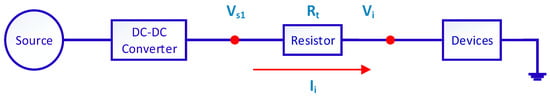
Figure 1.
Schematic diagram of the circuit for a conventional resistor hardness design.
The represents the resistor in the conventional method, which is connected at the output of the DC-DC buck converter. The denotes the output voltage of the converter. The and represent the voltage and current of the device, respectively. Thus, the is expressed as:
According to Equation (1), the resistor changes the device current by limiting the circuit current. The device current decreases as the resistance increases. It indicates that the higher the resistance, the lower the device’s latch-up current. However, the increase in resistance is limited, since it will result in a reduced voltage of the device. When the device’s voltage is below the normal voltage tolerance range, it will prevent the device from operating properly. Therefore, the resistor is subject to certain constraints in the actual latch-up hardness.
Based on the above resistive hardness principle in combination with the latch-up property, two constraints are derived [31,32,33]:
- Condition 1: The resistor does not affect the normal operation of the device. The operating voltage of the device should not exceed the normal voltage tolerance range. Otherwise the device cannot operate successfully. The voltage tolerance range is typical −10% to 10% of the rated voltage.
- Condition 2: Reduce the latch-up current to below the SEL holding current when the device is experiencing the latch-up [34,35,36]. According to the latch-up criterion, when the latch-up current drops below the latch-up maintenance point, the device will exit the latch-up state because the latch-up current cannot be maintained.
The traditional method of taking the resistance will be studied with respect to the constraints. As well, the range of resistance is researched to illustrate the latch-up hardness problem that exists with the conventional method. The 3.3 V CMOS process device is selected as the object of the study, i.e., = 3.3 V, then the voltage tolerance is −0.3 V~0.3 V.
The range of satisfying condition 1 in the conventional method is represented as:
where denotes the voltage tolerance. From Equation (2), it is known that has a harsh range of Ω owing to its small voltage tolerance range.
The range of resistance fulfilling condition 2 in the conventional method is expressed as:
where and represent the latch-up holding voltage and latch-up current, respectively. As the resistor is required to meet both the normal operation and to make the device exit the latch-up, it is obtained that . According to the test data of several devices, is about 1.32 V~2.45 V, which means that . Usually is 2~3 times and more than , as well as combined with the actual data, it is evident that . It indicates that the conventional method does not allow the device to exit the latch-up.
To address the limitation of the conventional method, the paper proposes a latch-up hardness design with a resistor placed in front of the DC-DC buck converter. The details of the proposed method will be described in the next section.
2.2. The Proposed Method
The section describes in detail the connection method, operating principle, design advantages, parameter model and resistance-taking the method of the proposed method. Emphasis will be placed on the design advantages of the proposed method to allow the device to exit the latch-up and the discussion of the resistor-taking method by building a parametric model.
2.2.1. Take the Device out of the Latch-Up
Figure 2 depicts the schematic circuit diagram of the proposed hardness method. The resistor employed in the proposed method is named , which is connected to the input of the DC-DC converter. indicates the supply voltage to which the converter is attached. and separately represent the input voltage and input current of the converter. Thus, is given as:
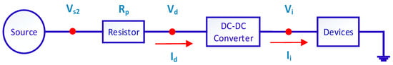
Figure 2.
Schematic diagram of the connection of the resistor in the proposed method.
From Equation (4), it is obvious that the proposed method operates by varying the input current of the DC-DC converter to regulate the current of the device. The hardness mechanism of is that reduces the device current by limiting the input current of the converter. As well, the device current decreases as the input current is reduced. However, compared to conventional design, the advantage of the proposed approach is that the objective of exiting the device from latch-up will be achieved by increasing the voltage tolerance based on the wide input range of the DC-DC converter. The input voltage range of the DC-DC buck converter is more extensive than the device’s voltage tolerance range, for example, the input range of LTM4644 converter is 2.4 V~14 V, which is much higher than the 0.3 V voltage tolerance of the 3.3 V device. The effect of a larger voltage tolerance is to make a larger range of resistance that satisfies condition 1. Following the operating principle of , it is known that a larger resistor makes the device latch-up current lower by further reducing the input current of the converter. When the device latch current falls below the latch-up holding current, the device will exit the latch-up.
2.2.2. Method of Taking the Resistance
To further investigate the proposed hardness method of taking the resistance that simultaneously meets conditions 1 and 2, a parametric model of the resistor placed at the input of the DC-DC buck converter is developed, as shown in Figure 3. The parametric model consists of supply voltage , resistor , switch S, inductor L, capacitor C, diode and feedback network. The feedback network is composed of resistors and , an error amplifier and a duty ratio modulator. The function of the feedback network is to generate the duty cycle signal and control the state of the switch.
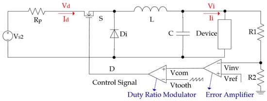
Figure 3.
Parametric model of the resistor placed at the input of the DC-DC buck converter.
According to the I-V characteristic of , is represented as:
where and denote the input voltage and input current of the DC-DC buck converter, respectively.
Following the DC-DC buck converter power conservation principle and duty cycle equation, it is known that:
where and respectively denote the conversion efficiency and duty cycle of the converter. and are related to the operating voltage and current of the converter which are available according to the datasheet or actual test values. Substituting Equations (6) and (7) into Equation (5) gives that:
From condition 1, the range of that satisfies the normal operation of the device is derived as:
where represents the equivalent resistance of the device in the normal state. indicates the minimum value of the device voltage in the voltage tolerance range. For 3.3 V devices, is typically 3.0 V.
The boundary formula for the meeting condition 2 is given by:
where signifies the equivalent resistance of the device in the latch-up state. In summary, the range of that simultaneously satisfies the normal operation of the device and enables the device to exit the latch-up is:
3. Pulsed Laser Experiments
3.1. Experimental Setup and Devices Selection
To verify the latch-up hardness performance of the proposed method and the method of taking the resistance, pulsed laser experiments are carried out. The mechanism of SEL induced by pulsed laser experiments in CMOS devices is approximately the same as that of heavy ion experiments, both of which induce latch-up in CMOS devices by ionization of electron-hole pairs. However, the primary differences between pulsed laser experiments and heavy ion experiments are the small spot diameter and high resolution of the pulsed laser, which allows accurate simulation of SEE caused by individual high-energy particles in space [37,38]. In addition, the irradiation intensity and irradiation time of CMOS devices by the pulsed laser are precisely controllable [39]. The pulsed laser test setup adopts the self-researched equipment of the National Space Science Centre of the Chinese Academy of Sciences. Figure 4 shows a schematic diagram of the pulsed laser unit. The laser setup consists of the component laser generator, the optical path system, the 3D mobile table, the synchronization control system and the host computer [40,41,42]. Table 1 shows the main parameters of the laser equipment.
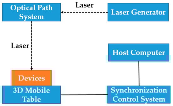
Figure 4.
A schematic diagram of the pulsed laser equipment.

Table 1.
The main parameters of the laser equipment.
Based on the operating principle and parametric model analysis of the proposed method, it is shown that the method in the paper is generally applicable to latch-up sensitive devices. To verify the applicability of the proposed method, two CMOS chips, A3PE1500 and AD7472, are selected as the test objects for laser experiments. Table 2 summarizes the key parameters of the two subjects. The normal operating and latch-up holding currents for device 1 are 0.072 A and 0.088 A respectively; for device 2 the normal operating and latch-up holding currents are 0.022 A and 0.031 A accordingly.
Table 2.
The key parameters of the two test subjects.
The devices will be triggered to produce the SEL when a pulsed laser is an incident on the active regions inside the devices. To ensure that the laser energy is effectively injected into the active areas, the devices must be back-opened before laser experiments. Figure 5 illustrates the practical picture of the devices in the pulsed laser experiments. The diagram contains mainly the pulsed laser, the devices and the DC-DC buck converter. The input of the DC-DC buck converter is connected to the supply voltage, and the output is attached to the power supply of the devices.
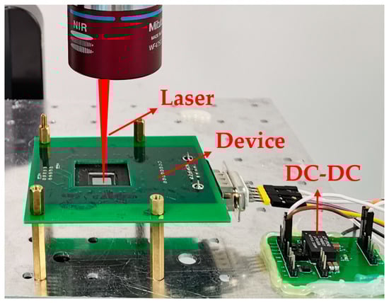
Figure 5.
The practical picture of the devices in the pulsed laser experiments.
3.2. Experimental Method
The purposes of the experiments are to verify that the proposed method enables the devices to exit the latch-up as well as the resistor-taking method. To better illustrate the experimental results, comparative tests are designed in the paper for the conventional and experimental groups respectively. The resistor of the conventional group is connected to the output of the DC-DC buck converter, while the resistor of the experimental group is attached to the input of the DC-DC buck converter. Besides, the experimental manipulation is the same for both. The experimental operation is divided into three major steps, which are adjusting the position of the devices to be tested, testing the functions of the devices and changing the resistance.
- First, the devices are adjusted to a horizontal state by adjusting the 3D moving table to ensure that the laser energy is injected into the devices at the same depth.
- Then, with the circuit connected correctly, the power is turned on to test the functions of the devices. The voltages and currents of the devices in the initial state and the latch-up state in the two sets of experiments are detected and recorded respectively.
- Finally, by connecting different resistors, the electrical parameters of the devices in the initial state and in the latch-up state are recorded in both sets of experiments.
When the initial voltages of the devices exceed the voltage tolerance range, it means that the resistance is already the maximum value, and the experiment will end at this time. The following experimental results will be obtained by collating the relevant test data.
3.3. Experimental Results
3.3.1. Exiting the Devices from the Latch-Up by the Proposed Method
To demonstrate that the proposed method enables the devices to exit the latch by increasing the resistance range, the section first investigates the resistance range of the proposed method compared to the conventional design. Next, a comparative analysis is performed on the latch-up currents variation over the range of resistance values.
Figure 6 depicts the ranges of the resistance under the conventional method and the proposed design, respectively. Figure 6a shows a resistance range of 0 to 8.2 Ω in the conventional method within the normal operating voltage range of device 1. The proposed method, however, has a resistance range of 0 to 41 Ω. In comparison to the conventional method, the proposed method increases the resistance range by up to 400%. Figure 6b depicts the resistance ranges of 0~14 Ω and 0~56 Ω for the conventional method and the proposed method, respectively, in the operating voltage range of device 2. A 300% increase in resistance range can be achieved with the proposed design. It is concluded that the proposed design improves the resistance range by 300% to 400%.
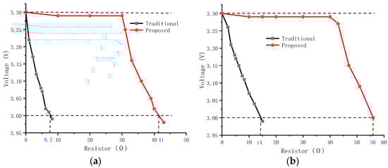
Figure 6.
The ranges of the resistance under the conventional method and the proposed design, respectively. (a) Description of the ranges of the resistance in device 1; (b) Description of the ranges of the resistance in device 2.
The increase in the resistance range will further improve the latch-up hardness of devices. Under certain conditions, the resistor will make the devices drop out of the latch-up. Figure 7 shows the relationships between the resistor and the latch-up current of the two devices under two different methods. Figure 7a describes the conventional method of reducing the device 1 latch-up current to 134.7 mA at resistor maximum. Even so, the device 1 remains in an abnormal latch-up state. Nevertheless, the proposed method reduces the device current to below the latch-up holding current of 72.1 mA at a resistance of 34 Ω. Consequently, the proposed hardness design with resistances of 34 Ω and above will keep device 1 from latch-up. Figure 7b illustrates that the conventional method and the proposed design respectively reduce the device 2 latch-up current to 50.3 mA and 24.2 mA (below the holding current). However the proposed method improves the latch-up hardness of the device by making it latch-up-free under certain conditions because of the large resistance range.
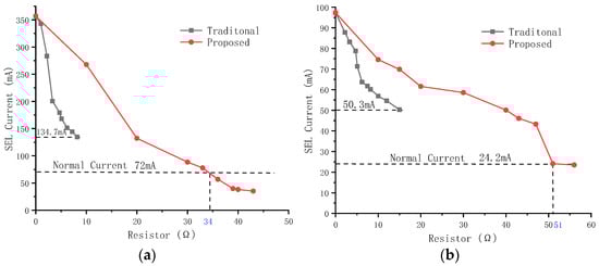
Figure 7.
Graph of resistance versus latch-up current for two devices under two different methods. (a) Relationship between resistance and latch-up current of device 1; (b) Relationship between resistance and latch-up current of device 2.
3.3.2. Verification of the Resistance-Taking Method
To verify the resistance range of the proposed method, the main parameters of devices in Table 2 are substituted into Equations (4) and (11) respectively. The theoretical range of resistance is calculated to be 37 Ω~48 Ω and 53 Ω~62 Ω for device 1 and device 2 separately. Table 3 indicates the theoretical and actual ranges of resistance. According to the experimental results in Figure 6, it can be seen that of the two devices are 0 Ω~41 Ω and 0 Ω~56 Ω, respectively. According to the data in Figure 7, it is evident that of the two devices are 34 Ω and above, and 51 Ω and above, accordingly.
Table 3.
The theoretical and actual ranges of resistance.
It is noticed that the actual results of the resistance are smaller than the theoretical results. This phenomenon may be due to the capacitor and inductor of the converter having parasitic resistance in the actual circuit, resulting in an actual low resistance.
4. Discussion of Resistor Power Consumption
The issue with the proposed method is that it will cause an increase in the power consumption of the circuits, due to the increased resistance range compared to the traditional design. Figure 8 summarizes the power consumption data of the proposed resistor versus the conventional resistor in the devices. The power consumption of the resistor in the proposed method is about 0.11 W to 0.19 W, which is more than 50% higher than that of the conventional design.
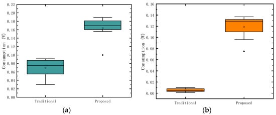
Figure 8.
Description of the power consumption generated by the resistor in the two devices with two different methods. (a) Displays the power consumption generated by the resistor in device 1; (b) Introduction of the power consumption generated by the resistor in device 2.
To reduce the power consumption problem of the proposed method, the approach of reducing the converter input voltage is proposed. The minimum input voltage of the DC-DC buck converter is above the device voltage, i.e., > 3.3 V. Therefore, 6 V, 5 V, and 4.5 V supply voltages are chosen to explore the effect of voltage reduction on resistor power consumption. Figure 9 shows the resistive power consumption for the two devices with supply voltages of 6 V, 5 V, and 4.5 V, correspondingly. It is observed that the resistive power consumption reduces with decreasing supply voltage. Compared to the resistor power consumption with a supply voltage of 6 V, the resistor power consumption with a supply voltage of 4.5 V is reduced by more than 87% to about 0.06 W~0.08 W. Power consumption is acceptable in engineering.
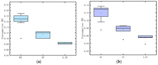
Figure 9.
Power consumption of the resistor at 6 V, 5 V, and 4.5 V for the two devices separately. (a) The power consumption generated by the resistor in device 1; (b) The power consumption generated by the resistor in device 2.
5. Conclusions
The paper proposes a circuit-level SEL hardness design for a resistor in front of a DC-DC buck converter. The method improves the latch-up hardness performance by improving the resistance range compared to the conventional hardness design. The proposed method enables devices to exit the latch-up when the resistance takes the value of . The proposed method is validated with the A3PE1500 and AD7472 CMOS devices to effectively increase the resistance range by 300% to 400%. It is also demonstrated that the resistor enables devices to operate normally and exit the latch-up within the boundary range when devices are suffering from SEL.
Author Contributions
Conceptualization, J.X. and J.H.; methodology, J.X., X.Z. and Y.M.; validation, J.X., Y.M., J.H. and X.Z.; formal analysis, J.X.; investigation, J.X.; resources Y.M. and X.Z.; data curation, J.X.; writing—original draft preparation, J.X.; writing—review and editing, J.X., Y.M. and X.Z.; visualization, J.X.; supervision, J.H., Y.M. and X.Z.; project administration, Y.M. and J.H.; funding acquisition, X.Z. All authors have read and agreed to the published version of the manuscript.
Funding
This research was funded by the National Natural Science Foundation of China (No. U2241280).
Data Availability Statement
The data used to support the findings of this study are available from the corresponding author upon request.
Acknowledgments
This work was supported by the Effects Centre of State Key Laboratory of Space Weather of the National Space Science Center, and research group members. The authors offer deep appreciation for their kind support.
Conflicts of Interest
The authors declare no conflict of interest.
References
- Guo, J.; Zhu, L.; Sun, Y.; Cao, H.; Huang, H.; Wang, T.; Qi, C.; Zhang, R.; Cao, X.; Xiao, L.; et al. Design of Area-Efficient and Highly Reliable RHBD 10T Memory Cell for Aerospace Applications. IEEE Trans. VLSI Syst. 2018, 26, 991–994. [Google Scholar] [CrossRef]
- Li, Z.; Berti, L.; Wouters, J.; Wang, J.; Leroux, P. Characterization of the Total Charge and Time Duration for Single-Event Transient Voltage Pulses in a 65-Nm CMOS Technology. IEEE Trans. Nucl. Sci. 2022, 69, 1593–1601. [Google Scholar] [CrossRef]
- Liu, J.; Zhou, Z.; Wang, D.; Zhou, S.-Q.; Sun, X.-M.; Ren, W.-P.; You, B.-H.; Gao, C.-S.; Xiao, L.; Yang, P.; et al. Prototype of Single-Event Effect Localization System with CMOS Pixel Sensor. Nucl. Sci. Tech. 2022, 33, 136. [Google Scholar] [CrossRef]
- Prasad, G.; Mandi, B.C.; Ali, M. Double-Node-Upset Aware SRAM Bit-Cell for Aerospace Applications. Microelectron. Reliab. 2022, 133, 114526. [Google Scholar] [CrossRef]
- Autran, J.L.; Moindjie, S.; Munteanu, D.; Dentan, M.; Moreau, P.; Pellissier, F.P.; Bucalossi, J.; Borgese, G.; Malherbe, V.; Thery, T.; et al. Real-Time Characterization of Neutron-Induced SEUs in Fusion Experiments at WEST Tokamak During D-D Plasma Operation. IEEE Trans. Nucl. Sci. 2022, 69, 501–511. [Google Scholar] [CrossRef]
- Roffe, S.; Akolkar, H.; George, A.D.; Linares-Barranco, B.; Benosman, R.B. Neutron-Induced, Single-Event Effects on Neuromorphic Event-Based Vision Sensor: A First Step and Tools to Space Applications. IEEE Access 2021, 9, 85748–85763. [Google Scholar] [CrossRef]
- Biereigel, S.; Kulis, S.; Leroux, P.; Moreira, P.; Kolpin, A.; Prinzie, J. Single-Event Effect Responses of Integrated Planar Inductors in 65-Nm CMOS. IEEE Trans. Nucl. Sci. 2021, 68, 2587–2597. [Google Scholar] [CrossRef]
- Biereigel, S.; Kulis, S.; Moreira, P.; Kölpin, A.; Leroux, P.; Prinzie, J. Radiation-Tolerant All-Digital PLL/CDR with Varactorless LC DCO in 65 Nm CMOS. Electronics 2021, 10, 2741. [Google Scholar] [CrossRef]
- Monda, D.; Ciarpi, G.; Saponara, S. Diagnosis of Faults Induced by Radiation and Circuit-Level Design Mitigation Techniques: Experience from VCO and High-Speed Driver CMOS ICs Case Studies. Electronics 2021, 10, 2144. [Google Scholar] [CrossRef]
- Wang, Y.; Liu, F.; Li, B.; Li, B.; Huang, Y.; Yang, C.; Zhang, J.; Wang, G.; Luo, J.; Han, Z.; et al. Dependence of Temperature and Back-Gate Bias on Single-Event Upset Induced by Heavy Ion in 0.2-Μm DSOI CMOS Technology. IEEE Trans. Nucl. Sci. 2021, 68, 1660–1667. [Google Scholar] [CrossRef]
- Ladbury, R.; Bay, M.; Zinchuk, J. Threats to Resiliency of Redundant Systems Due to Destructive SEEs. IEEE Trans. Nucl. Sci. 2021, 68, 970–979. [Google Scholar] [CrossRef]
- Gardenghi, R.A.; Houlne, R.C. Power Supply Considerations for Pulsed Solid-State Radar. In Proceedings of the Nineteenth IEEE Symposium on Power Modulators, San Diego, CA, USA, 26–28 June 1990; IEEE: San Diego, CA, USA, 1990; pp. 146–152. [Google Scholar]
- Kohinata, H.; Arai, M.; Fukumoto, S. An Experimental Study on Latch Up Failure of CMOS LSI. In Proceedings of the 2008 Second International Conference on Secure System Integration and Reliability Improvement, Yokohama, Japan, 14–17 July 2008; IEEE: Yokohama, Japan, 2008; pp. 215–216. [Google Scholar]
- Yu, Y.; Biess, J.J. Some Design Aspects Concerning Input Filters for DC-DC Converters. In Proceedings of the 1971 IEEE Power Electronics Specialists Conference, Pasadena, CA, USA, 19–20 April 1971; IEEE: Pasadena, CA, USA, 1971; pp. 66–76. [Google Scholar]
- Liang, S.; Hou, L.Z.; Gu, T.; Salama, C.A.T. Latch-up Modeling of BiCMOS Merged Bipolar-MOS Structures. Solid State Electron. 1992, 35, 1461–1469. [Google Scholar] [CrossRef]
- Duzellier, S. Radiation Effects on Electronic Devices in Space. Aerosp. Sci. Technol. 2005, 9, 93–99. [Google Scholar] [CrossRef]
- Cecchetto, M.; García Alía, R.; Wrobel, F. Impact of Energy Dependence on Ground Level and Avionic SEE Rate Prediction When Applying Standard Test Procedures. Aerospace 2019, 6, 119. [Google Scholar] [CrossRef]
- Hiblot, G.; Serbulova, K.; Hellings, G.; Chen, S.-H. TCAD Study of Latch-up Sensitivity to Wafer Thinning below 500 Nm. In Proceedings of the 2021 International Semiconductor Conference (CAS), Sinaia, Romania, 6–8 October 2021; IEEE: Sinaia, Romania, 2021; pp. 121–124. [Google Scholar]
- Osipenko, P.N.; Antonov, A.A.; Klishin, A.V.; Vasilegin, B.V.; Gorbunov, M.S.; Dolotov, P.S.; Zebrev, G.I.; Anashin, V.S.; Emeliyanov, V.V.; Ozerov, A.I.; et al. Fault-Tolerant SOI Microprocessor for Space Applications. IEEE Trans. Nucl. Sci. 2013, 60, 2762–2767. [Google Scholar] [CrossRef]
- Dodds, N.A.; Hooten, N.C.; Reed, R.A.; Schrimpf, R.D.; Warner, J.H.; Roche, N.J.; McMorrow, D.; Wen, S.; Wong, R.; Salzman, J.F.; et al. Effectiveness of SEL Hardening Strategies and the Latchup Domino Effect. IEEE Trans. Nucl. Sci. 2012, 59, 2642–2650. [Google Scholar] [CrossRef]
- Jiang, Z.-H.; Ker, M.-D. Schottky-Embedded Isolation Ring to Improve Latch-Up Immunity Between HV and LV Circuits in a 0.18 Μm BCD Technology. IEEE J. Electron Devices Soc. 2022, 10, 516–524. [Google Scholar] [CrossRef]
- Tsai, H.-W.; Ker, M.-D. Active Guard Ring to Improve Latch-Up Immunity. IEEE Trans. Electron Devices 2014, 61, 4145–4152. [Google Scholar] [CrossRef]
- Chen, C.-C.; Ker, M.-D. Optimization Design on Active Guard Ring to Improve Latch-Up Immunity of CMOS Integrated Circuits. IEEE Trans. Electron Devices 2019, 66, 1648–1655. [Google Scholar] [CrossRef]
- Jiang, Z.-H.; Ker, M.-D. Latch-Up Prevention with Autodetector Circuit to Stop Latch-Up Occurrence in CMOS-Integrated Circuits. IEEE Trans. Electromagn. Compat. 2022, 64, 1785–1792. [Google Scholar] [CrossRef]
- Tsai, H.-W.; Ker, M.-D. Latch-Up Protection Design with Corresponding Complementary Current to Suppress the Effect of External Current Triggers. IEEE Trans. Device Mater. Relib. 2015, 15, 242–249. [Google Scholar] [CrossRef]
- Becker, H.N.; Miyahira, T.F.; Johnston, A.H. Latent Damage in CMOS Devices from Single-Event Latchup. IEEE Trans. Nucl. Sci. 2002, 49, 3009–3015. [Google Scholar] [CrossRef]
- Jeong, S.-H.; Lee, N.-H.; Cho, S.-I. A Design of High-speed Power-off Circuit and Analysis. Trans. Korean Inst. Electr. Eng. 2014, 63, 490–494. [Google Scholar] [CrossRef]
- Andjelković, M.S.; Petrović, V.; Stamenković, Z.; Ristić, G.S.; Jovanović, G.S. Circuit-Level Simulation of the Single Event Transients in an On-Chip Single Event Latchup Protection Switch. J. Electron. Test. 2015, 31, 275–289. [Google Scholar] [CrossRef]
- Rui, C.; Ying, F.; Yongtao, Y.; Shipeng, S.G.; Guoqiang, F.; Xiang, Z.; Yingqi, M.; Jianwei, H. Mitigation Technique and Experimental Verification of Single Event Latch-up Effect in Circuit Level for CMOS Device. At. Energy Sci. Technol. 2014, 48, 721–726. [Google Scholar]
- Niaraki Asli, R.; Shirinzadeh, S. High Efficiency Time Redundant Hardened Latch for Reliable Circuit Design. J. Electron. Test. 2013, 29, 537–544. [Google Scholar] [CrossRef]
- Ball, D.R.; Sheets, C.B.; Xu, L.; Cao, J.; Wen, S.-J.; Fung, R.; Cazzaniga, C.; Kauppila, J.S.; Massengill, L.W.; Bhuva, B.L. Single-Event Latchup in a 7-Nm Bulk FinFET Technology. IEEE Trans. Nucl. Sci. 2021, 68, 830–834. [Google Scholar] [CrossRef]
- Li, D.; Liu, T.; Wu, Z.; Cai, C.; Zhao, P.; He, Z.; Liu, J. An Investigation of FinFET Single-Event Latch-up Characteristic and Mitigation Method. Microelectron. Reliab. 2020, 114, 113901. [Google Scholar] [CrossRef]
- Yongtao, Y.; Guoqiang, F.; Rui, C.; Shipeng, S.G.; Jianwei, H. Experimental Study on Single Event Latchup of SRAM K6R4016V1D and Its Protection. At. Energy Sci. Technol. 2012, 46, 587–591. [Google Scholar]
- Matino, H. Analysis of the holding current in CMOS latch-up. IBM J. Res. Dev. 1985, 29, 588–592. [Google Scholar] [CrossRef]
- Mergens, M.P.J.; Russ, C.C.; Verhaege, K.G.; Armer, J.; Jozwiak, P.C.; Mohn, R. High Holding Current SCRs (HHI-SCR) for ESD Protection and Latch-up Immune IC Operation. Microelectron. Reliab. 2003, 43, 993–1000. [Google Scholar] [CrossRef]
- Chen, M.-J.; Lee, H.-S.; Chen, J.-H.; Hou, C.-S.; Lin, C.-S.; Jou, Y.-N. A Physical Model for the Correlation between Holding Voltage and Holding Current in Epitaxial CMOS Latch-Up. IEEE Electron Device Lett. 1998, 19, 276–278. [Google Scholar] [CrossRef]
- Burnell, A.J.; Chugg, A.M.; Harboe-Sørensen, R. Laser SEL Sensitivity Mapping of SRAM Cells. IEEE Trans. Nucl. Sci. 2010, 57, 1973–1977. [Google Scholar] [CrossRef]
- Faraud, E.; Pouget, V.; Shao, K.; Larue, C.; Darracq, F.; Lewis, D.; Samaras, A.; Bezerra, F.; Lorfevre, E.; Ecoffet, R. Investigation on the SEL Sensitive Depth of an SRAM Using Linear and Two-Photon Absorption Laser Testing. IEEE Trans. Nucl. Sci. 2011, 58, 2637–2643. [Google Scholar] [CrossRef]
- Jones, R.; Chugg, A.M.; Jones, C.M.S.; Duncan, P.H.; Dyer, C.S.; Sanderson, C. Comparison between SRAM SEE Cross-Sections from Ion Beam Testing with Those Obtained Using a New Picosecond Pulsed Laser Facility. IEEE Trans. Nucl. Sci. 2000, 47, 539–544. [Google Scholar] [CrossRef]
- Feng, G.; Shangguan, S.; Ma, Y.; Han, J. SEE Characteristics of Small Feature Size Devices by Using Laser Backside Testing. J. Semicond. 2012, 33, 014008. [Google Scholar] [CrossRef]
- Chen, R.; Han, J.-W.; Zheng, H.-S.; Yu, Y.-T.; Shangguang, S.-P.; Feng, G.-Q.; Ma, Y.-Q. Comparative Research on “High Currents” Induced by Single Event Latch-up and Transient-Induced Latch-Up. Chin. Phys. B 2015, 24, 046103. [Google Scholar] [CrossRef]
- Yingqi, M.; Jianwei, H.; ShiPeng, S.; Rui, C.; Xiang, Z.; Yue, L.; Yueying, Z. SEE Characteristics of COTS Devices by 1064 nm Pulsed Laser Backside Testing. In Proceedings of the 2018 IEEE Nuclear & Space Radiation Effects Conference (NSREC 2018), Waikoloa Village, HI, USA, 16–20 July 2018; IEEE: Waikoloa Village, HI, USA, 2018; pp. 1–4. [Google Scholar]
Disclaimer/Publisher’s Note: The statements, opinions and data contained in all publications are solely those of the individual author(s) and contributor(s) and not of MDPI and/or the editor(s). MDPI and/or the editor(s) disclaim responsibility for any injury to people or property resulting from any ideas, methods, instructions or products referred to in the content. |
© 2023 by the authors. Licensee MDPI, Basel, Switzerland. This article is an open access article distributed under the terms and conditions of the Creative Commons Attribution (CC BY) license (https://creativecommons.org/licenses/by/4.0/).