1. Introduction
Currently, the development of acousto-electronic sensors intended for various applications such as biology, fine physicochemical studies, analysis of the gas composition of the atmosphere, and detection of explosives is in active progress. There are many approaches to solving this problem. Using modern technologies, one can detect the adsorption of a single gas molecule. For example, in [
1], the concentration of various gases was recorded at the level of one ppb. This high resolution was achieved due to the unique sensory properties of graphene. Most of the known acoustic sensory methods register changes in the resonant frequency of the device as an oscillating plate, a cantilever made of silicon, and resonators based on the surface (SAW) or bulk acoustic waves (hereinafter referred to as the BAW resonator). The record sensitivity of mass measurement of several attograms was demonstrated in [
2,
3]. Using a cantilever’s frequency shift vs. mass load, the mass value of the smallpox virus of about 12 fg was found [
2]. The authors in [
4] described an application of the nanoelectromechanical system (NEMS) device to ultrasensitive mass detection and measured the Au film mass deposition with the resolution of some attograms. Such sensors had to satisfy the high demands of the experiment arrangement such as a high vacuum and precise temperature control at low temperatures. A special problem is the one-time use of the NEMS sensory element. In addition, there has always been a question about the complicated calibration procedure of that device. Thus, the search for analogs, which are simpler and more convenient in a practical sense, remains open. Acousto-electronic sensor devices have some advantages in this field.
The most known and widely employed sensor is the so-called quartz crystal microbalance (QCM) which was first developed by Sauerbrey [
5]. This device consists of a quartz plate with metal electrodes deposited on the main surface, i.e., there is a piezoelectric resonator with the longitudinal or shear bulk acoustic waves as operational modes. The reduced mass sensitivity of such devices changes from 10
8–10
10 Hz·cm
2/g [
6,
7]. The authors of [
6] showed that the relative frequency shift under the large mass load deviated from the linearly proportional dependence and depended on the acoustical impedance ratio of quartz and deposited film. The QCM device has been employed for studying metal film deposition, electroplated alloy etching rate, oxidation processes of metal film, and the physical properties of the solid–liquid interfacial layer in situ [
8]. Other well-known sensor schemes are based on the properties of SAW resonators. Their sensitivity has the typical value of about 2.5 × 10
−9 Hz·cm
2/g [
9]. The film bulk acoustic resonator (FBAR) as a sensor has the typical value of mass sensitivity about 3.6 × 10
−6 Hz·cm
2/g [
10]. A given device showed a thickness sensitivity to the deposition of the Ti film of about 1.6 nm, achieved at an operating frequency of about 2442 MHz. Furthermore, small sensory devices based on microelectromechanical systems (MEMS) have been developed. For example, a MEMS FBAR-based mass sensor built on a micromachined silicon nitride diaphragm and operating in vapor and liquid had a mass sensitivity of 726 cm
2/g, which is about 50 times than that of a typical quartz crystal microbalance [
11]. However, the quality factor
Q of such a device in air was about 200–300 at 1 GHz and dropped to about 40 at 2 GHz. This would lead to a drop in the sensor’s sensitivity. In [
12], the possibility of using a thin-film acoustic resonator with a Bragg reflective grating as a sensor of organic films was considered. Operating frequencies of 6–8 GHz were used. The authors [
13] investigated the use of an FBAR sensor with a shear operating mode for studying the properties of liquids. At a resonant frequency of 1.25 GHz in water, the
Q-factor of the resonator decreased to 150 from the value of 300 in air. It should be noted that both membrane FBAR sensors and those developed using MEMS or NEMS technology have one common disadvantage in that they cannot be reused.
Mansfel’d et al. [
14] proposed the high overtone bulk acoustic resonator (HBAR) for the spectroscopy of metal film properties. The authors of [
15] proposed an experimental and model investigation of the sensory properties of HBAR structures as “AlN/SiO
2” and “YX
l/163°LiNbO
3/YX
l/32° quartz” operating in longitudinal (L) and shear (S) bulk acoustic modes, respectively. The main objective consisted of improving the HBAR’s gravimetric (mass) sensitivity. The peculiarities of BAW reflection and penetration into deposited films were established. However, in our opinion, the HBAR’s sensory properties were insufficiently studied. Hence, owing to HBAR’s high quality factor in the microwave band, one can get increasing sensitivity taking into account the high operational frequency which will sufficiently exceed that in SAW- or FBAR-based sensors. However, such an opportunity can only be realized if the substrate’s material possesses low acoustic attenuation in the microwave frequency band, e.g., diamond [
16]. Here, diamond’s excellent acoustic properties were investigated in the microwave band up to 20 GHz. It is shown that the diamond-based HBAR’s quality factor of about 12,500 at ~20 GHz remained at such a high value only owing to Landau–Rumer’s mechanism of microwave acoustic attenuation in diamond [
17]. The L-BAW excitation of the diamond-based HBAR in the extremely high frequency band up to 40 GHz was published in [
18]. A quality factor of ~10,000 at 40 GHz was obtained. Recently, we obtained a Patent RF dedicated to the diamond-based microwave acoustic mass sensor [
19]. Earlier, by means of diamond-based HBAR as a sensor, the deposition of thin and ultrathin metal films such as Mo, Al,Sc, and Pt was experimentally studied [
20,
21,
22]. A new useful approach for analyzing the wave propagation in piezoelectric nano-size plates under special boundary conditions was proposed in [
23]. According to [
24], in the future, super-thin films, smart materials, and smart nanodevices will replace macro-sized elements in conventional acoustic devices. Thus, to design and build such novel elements, it is necessary to have models of acoustic wave propagation in small-scale environments while taking into account several factors.
This work makes the following contributions: (i) the experimental Q-factor’s dependences on the film thickness are introduced and discussed; (ii) the HBAR-based sensor model is proposed and studied in detail using FEM; (iii) a complete explanation of the peculiarities of the BAW propagation in diamond-based MPSs under the influence of a certain metal film deposition is provided.
Therefore, the main objective of this work was concerned with a detailed study of the properties and opportunities of acousto-electronic sensors based on microwave HBAR with a diamond substrate, including a model visualization of acoustic wave propagation and the conditions of optimal sensitivity.
2. Materials and Methods
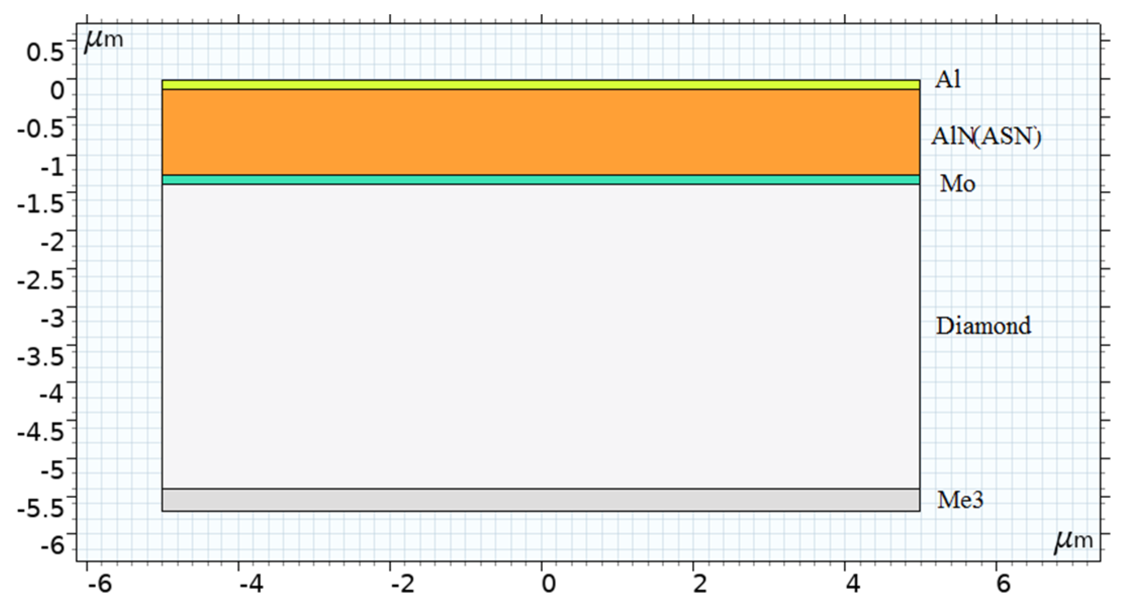
The HBAR-based sensors were realized using the “Me1/AlN/Me2/(001) diamond/Me3” or “Me1/(Al,Sc)N/Me2/(001) diamond/Me3” multilayered piezoelectric structures (MPS). Here, Me1 and Me2 are metallic electrodes such as Al, Mo, or Pt, and Me3 is the deposited metal film to be studied. The technology of the “Al/AlN/Mo/diamond” HBAR processing was described in detail in [
21]. As a substrate, plates made of type IIa synthetic single-crystalline diamond produced by FSBI TISNCM were applied. Piezoelectric films of aluminum nitride AlN and aluminum–scandium nitride (Al,Sc)N were used in the thin-film piezoelectric transducers (TFPT) as Me1/AlN/Me2 or Me1/(Al,Sc)N/Me2 to excite the longitudinal bulk acoustic wave (L-BAW). However, the application of aluminum–scandium nitride leads to more effective electromechanical excitation of L-BAW as an HBAR operational mode even in the extremely high-frequency band [
18].
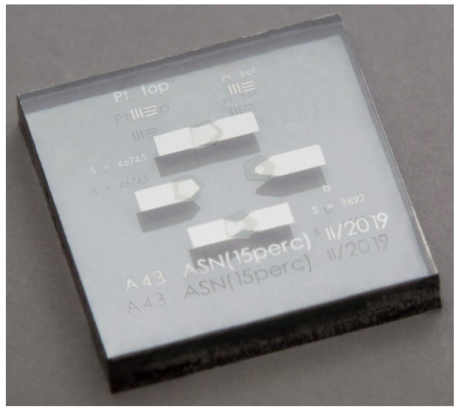
Figure 1 represents an example of such a sensory element based on the MPS “Pt/(Al,Sc)N/Pt/(001) diamond” (Sc content 15%). There, one can see the four independent HBARs distinguished by the area of an active zone, hereafter titled an aperture. One of them, with the aperture of 10,000 sq. microns, was used as sensor #C. The main parameters of the sensory elements studied are given in
Table 1.
To evaluate how different acoustic impedance affects the performance of a diamond-based sensor, three metals with widely varying acoustic properties were selected. A comparison of the acoustic characteristics of studied metals, including diamond, is presented in
Table 2. Here,
Z = ρ
V, where ρ is the material density, and
V is the L-BAW phase velocity.
The metal films were deposited on the free side of the diamond substrate by the AJA Orion 8 magnetron sputtering equipment, which was used to fabricate the HBARs themselves. The number of layers varied from six to 40 in different approaches. The substrate holder was rotated with an angular speed of 1 rad/min. In the case of thin layers, h < 20 nm, the angular speed was increased to 2 rad/min. The unevenness of the thickness of the deposited films was less than 5% over the entire surface of the substrate holder. The mean film growth rate was equal to ~100 nm/h.
The thickness of deposited films in the sputtering process was controlled by a QCM sensor installed in the magnetron chamber. For more precise thickness measurement, the atomic force microscope (AFM) method for accompanying Si samples was used. The metal was sputtered using the same process as for the HBAR sensor. The measurement uncertainty of the AFM method was from 10 nm to 3 nm. When the thickness of films was thinner than 5 nm, it was estimated from the deposition time with linear interpolation using a known growth rate.
When a metal film was sputtered, the sensor was extracted from the magnetron chamber and brought to the probe station. After that, the shift of the overtone’s resonant frequency and quality factors were measured. The process of the frequency response measurement of HBAR by the E5071C Agilent network analyzer was described in detail in [
18]. The operational checkpoint frequencies were selected for every sensor separately, and the overtones with the highest quality factor or highest impedance response were prioritized. When the measurement for the
n-th layer was over, the sensor was brought back to the magnetron chamber, and layer
n + 1 was sputtered.
To explain the data obtained, a computer simulation of acoustic wave propagation in MPSs using the COMSOL Multiphysics software was executed. For 2D MPS modeling, the diamond substrate and deposited films with a width of 10 μm were used (
Figure 2). This choice made it possible to reduce the number of calculations without a noticeable deviation from the qualitative and quantitative results of the experiment. Periodic type boundary conditions were applied. The maximum size of the grid cell did not exceed 1/10 of the elastic wavelength within a given particular layer.
3. Results
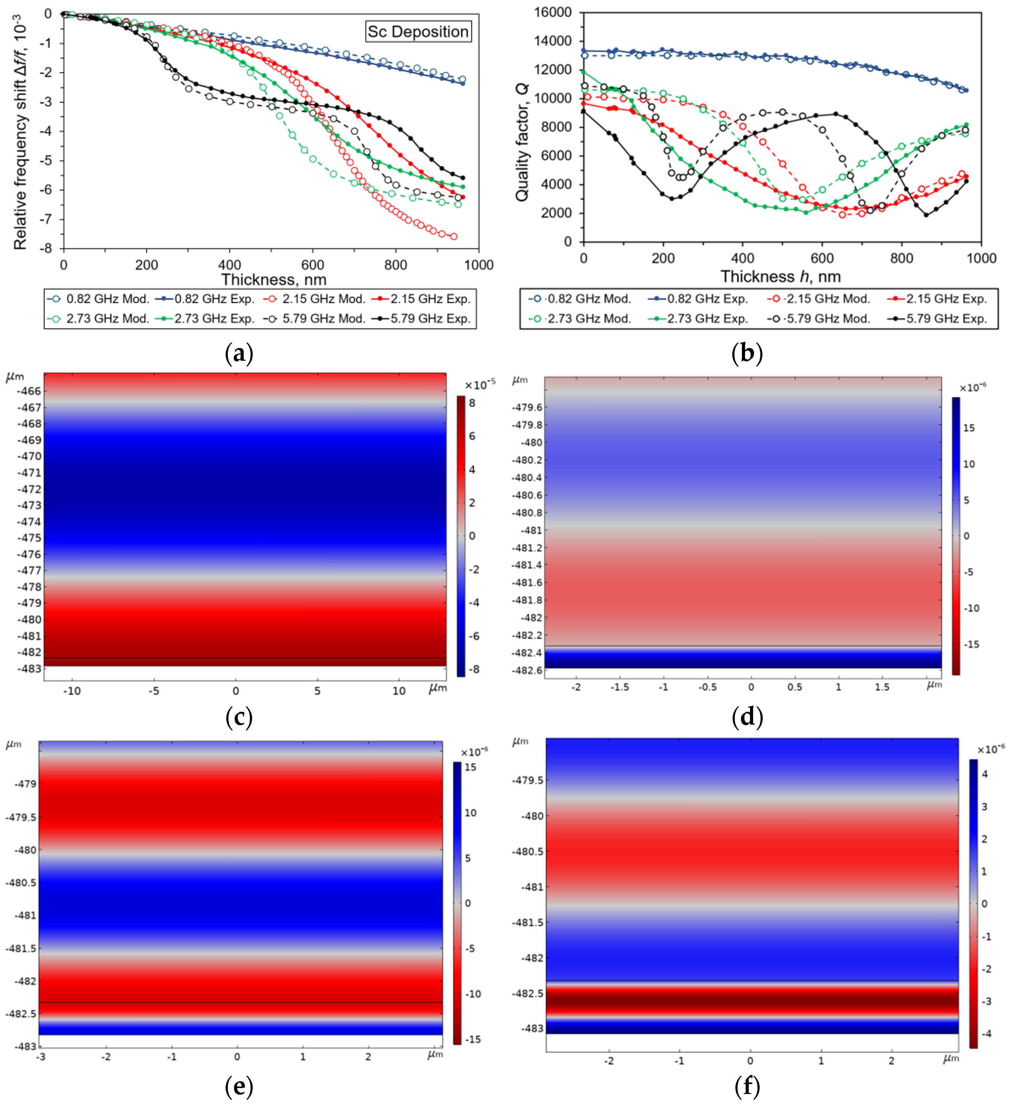
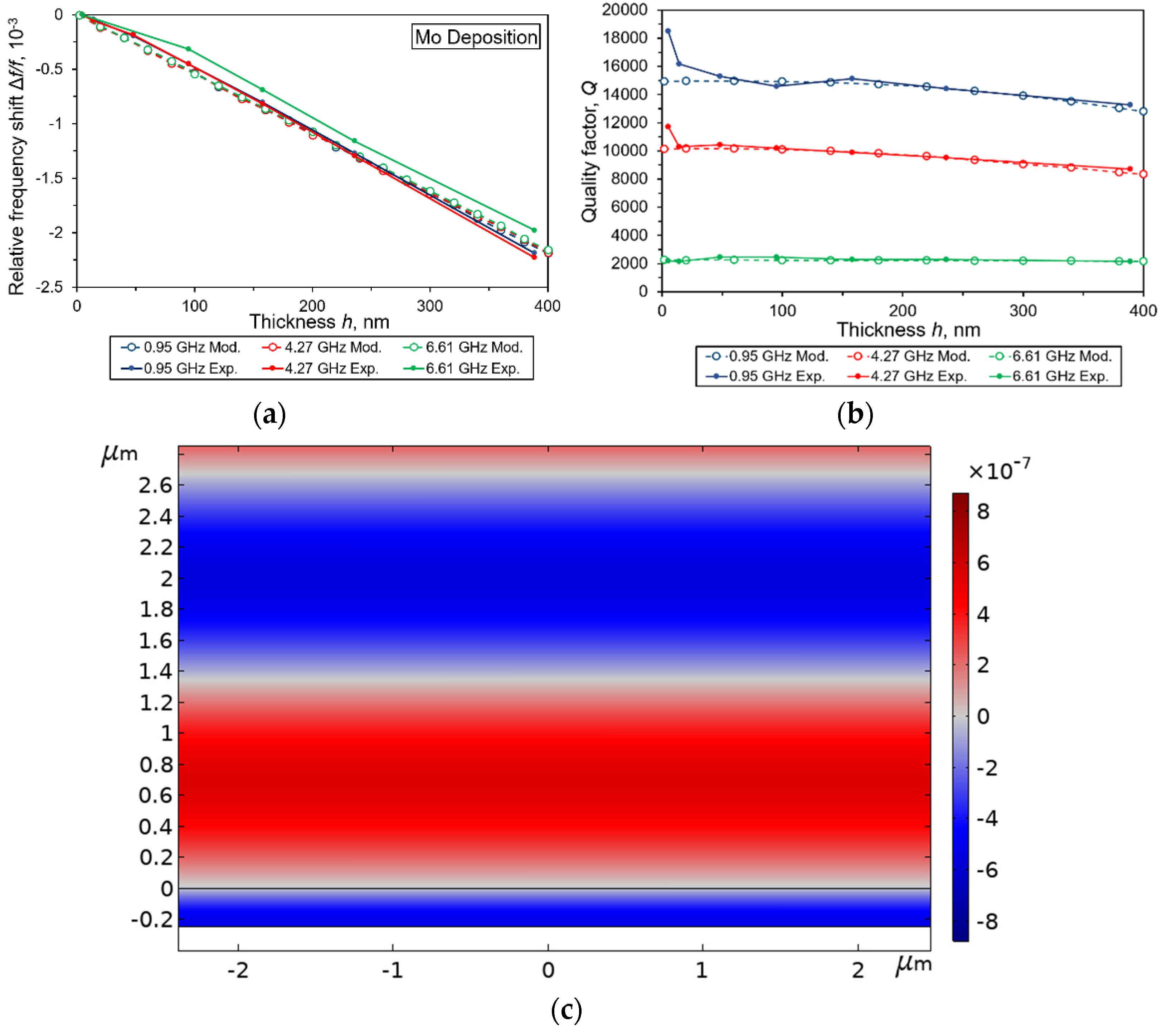
The enhanced experimental data, including the relative frequency shifts and quality factors vs. the thickness of a deposited film, are presented in
Figure 3,
Figure 4 and
Figure 5. Here, the results of finite element modeling by COMSOL Multiphysics software are also shown. In FEM calculations, the actual thicknesses of all the piezoelectric and metal films and diamond substrates as in the experiment were applied. The thickness ranges of film deposition (in nm) were changed within 0–950 for scandium, 0–390 for molybdenum, and 0–160 for platinum. The choice of operational acoustic overtones was fulfilled under the criterion of a maximal
Q-factor of an HBAR at the specified resonant frequencies. The basis is that the frequency response of an HBAR is closely concerned with the TFPT frequency dependence, where the minimal and maximal
Q values should be observed in the vicinity of the points where the conditions
or
are fulfilled, respectively. Here,
d is the TFPT thickness, λ is the wavelength in piezoelectric material, and
n = 1, 3, …;
m = 1, 2, … For more detail, see [
20]. An example of a mentioned dependence is presented in
Figure 5e. Owing to the high
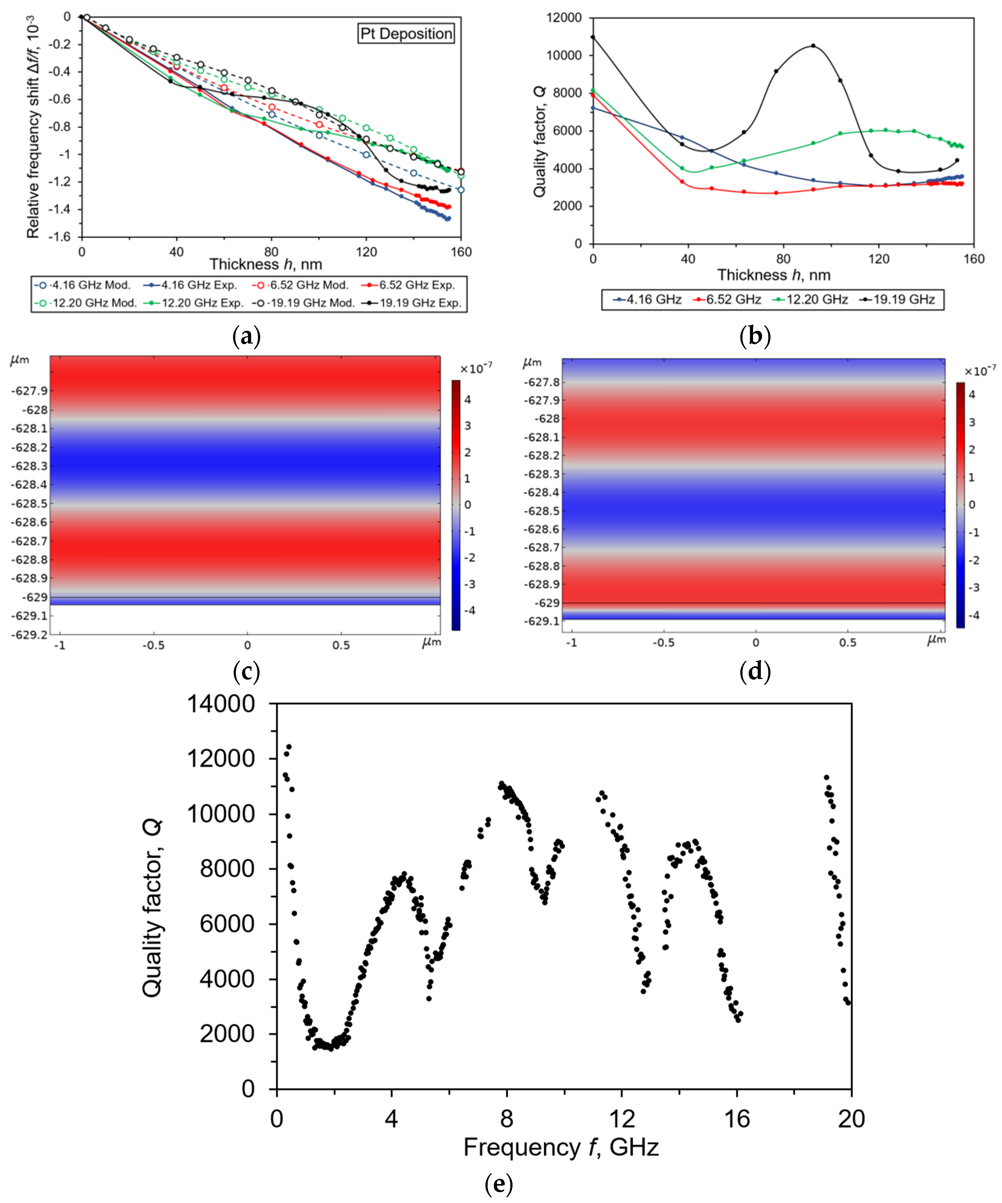
Q values, this HBAR can be used as a sensory element in the frequency range from 1 GHz up to 20 GHz.
The dependencies of frequency shift vs. the thickness of the different metal films change as a function of the relation between the acoustic impedances of diamond and a given film material. Therefore, one should consider three situations: (1) the metal Sc obeys the inequality Zdiam > ZSc; (2) the metal Mo obeys the approximate equality Zdiam ≈ ZMo; (3) the metal Pt obeys the inequality Zdiam < ZPt.
Figure 3a,b represent the relative frequency shift and quality factor vs. the Sc film thickness measured for the microwave acoustic overtones taken at four operational frequencies of 0.82 GHz, 2.15 GHz, 2.73 GHz, and 5.79 GHz of sensor #A. There, one can see the complicated dependencies of
and
Q =
f(
h) at the 2.15 GHz overtone and higher (
Figure 3a,b).
Figure 3c–f demonstrate the model distribution of the L-BAW vertical Y-components of elastic displacements taken at unusual points as the inflections of curves
and extremums of the
Q =
f(
h) dependencies. The sensor’s locations are shown only on the bottom side of an HBAR, including the Me3 deposited film. The red and blue patterns denote that the displacements were directed up or down, respectively. Thus, the distance between the corresponding red and blue points coincides with the λ/2 value of the L-BAW in a given material at a selected frequency. Analyzing
Figure 3d–f, one can say that, at the resonant frequency of 5.79 GHz, the λ/4, λ/2, and 3λ/4 values fit within the Sc thicknesses as 250 nm, 500 nm, and 750 nm, respectively. When
h = λ/4, the part of the L-BAW energy that penetrates into the deposited film reflects from a free film surface. As a result, the acoustic wave passes exactly a half wavelength within a film. This wave then interferes in the antiphase with a wave reflected out of the film–diamond interface. Hence, the interference minimum and a decrease in reflectance should be observed. This phenomenon is quite similar to the single-layer antireflection coating in optic devices. In the condition
h = λ/2, a bulk acoustic wave penetrates from diamond into the Sc film and then reflects from its free surface. Rereflection within the Sc free surface and Sc–diamond interface is also observed. In this case, the resonance phenomenon is directly observed in the deposited film. It should be emphasized that the
Q-factor is approximately the same as in the initial state of the sensor (
h = 0). In contrast,
Figure 3c shows the absence of such peculiarities at 0.82 GHz because λ >>
h.
As a result of Mo film deposition, only a linearly proportional dependence of the relative frequency shift on film thickness up to ~400 nm was observed for some operating frequencies up to 6.6 GHz, as shown in
Figure 4a. Let us take into account the approximate equality
ZMo ≈ Z
diam. In fact, in this case, one can talk about the elongation of a wave propagation path in the “diamond–Mo” composite structure only. Thus, the dependence of the relative frequency shift vs. thickness is proportional. The measured dependence turned out to be quite close to the forecast obtained using FEM analysis.
Figure 5a,b represent the relative frequency shift and quality factor vs. the Pt film thickness measured for the microwave acoustic overtones taken at four operational frequencies of 4.16 GHz, 6.52 GHz, 12.20 GHz, and 19.19 GHz of sensor #C. At 4.16 GHz and 6.52 GHz, monotonic and close to proportional dependences
can be observed. As in the case of Sc film deposition, there one can see the complicated dependencies
and
Q =
f(
h) at the 12.12 GHz and 19.19 GHz overtones.
Figure 5c,d demonstrate the model distribution of the L-BAW vertical Y-components of elastic displacements taken at the points of the inflections of curves
and extremums of the
Q =
f(
h) dependences. As an example, one can say that the λ/4 and λ/2 values fit within the Pt thicknesses as ~45 nm and ~90 nm at 19.19 GHz, respectively. Similar to the Sc film case, in the condition
h = λ/2, a bulk acoustic wave penetrates from diamond into the Pt film and then reflects from its free surface resonating in the film directly. The
Q-factor is approximately the same as in the initial state of a sensor (
h = 0).
4. Discussion
Theoretical and experimental results of microwave acoustic wave propagation in diamond-based multilayer piezoelectric structures as “Me1/(Al,Sc)N/Me2/(100) diamond/Me3” and “Me1/AlN/Me2/(100) diamond/Me3” under three metal film depositions were obtained. The relatively small decrease in the quality factor of diamond-based HBARs under the metal layer effect observed in a wide microwave band up to 20 GHz could be qualified as an important result. Changes in operational resonant frequencies vs. film thickness were discovered to have sufficient distinctions.
From the comparison of the Δ
f/
f =
f(
h) dependences for the Sc, Mo, and Pt deposited films (
Figure 3a,
Figure 4a and
Figure 5a), it follows that the HBAR-based sensor had the best sensitivity to changes in a Me3 film thickness nearby the points when
hMe3 ≈
nλ/4 (
n = 1, 3, 5, …) for metals with acoustic impedance satisfying
ZMe3 <
Zdiam. For metals with
ZMe3 > Z
diam, the highest sensitivity was observed at the points when
hMe3 ≈
mλ/2 (
m = 1, 2, 3, …). The more the impedance of a film differs from the impedance of the diamond substrate, the higher the sensor’s sensitivity is.
The explanation of Δ
f/
f =
f(
h) and
Q(
h) dependences is based on the difference in the reflection coefficients
R of an elastic wave reflected on the substrate–film interface due to the difference in their acoustic impedances [
25]. At
ZMe3 <
Zdiam, when the acoustic wave reflects from a film in the condition
hMe3 ≈
nλ/4, the reflection coefficient tends to zero, and the wave’s phase changes by 180°. The waves that pass into the film experience multiple reflections from the substrate–film interface and the outer surface of a film. At the outer surface of the film, all these waves add up in phase. As a result, an increase in the amplitude of their oscillations occurs. This effect leads to significant energy dissipation under the repeated passage of a wave through the thickness of a film. In this case, the quarter-wave film becomes a strong absorber of sound waves. As a result, the decrease in the Q-factor of an HBAR-based sensor is observed experimentally (
Figure 3b and
Figure 5b).
Under the condition
ZMe3 > Z
diam at the points of
hMe3 ≈
mλ/2, the
R-coefficient for a wave reflected from a film into diamond substrate has the maximal value. In this case, this coefficient is equal to the
R-coefficient for a wave reflected from the free substrate boundary. Since the transparency coefficient
T = 1 −
R of the film drops to zero, there is a kind of “shutdown” of a film, according to Brekhovskikh [
25]. As a result, the
Q-factor of the HBAR-based sensor remains approximately the same as in the absence of a film (
Figure 5b).
The slight decrease in Q-factor observed in the frequency range up to 20 GHz, excluding the abovementioned special points, is due to the fact that the Q-factor in HBAR is mainly determined by the ratio of stored energy to its dissipation over a period. Because the diamond substrate has the largest reserve of elastic energy, and the Landau–Rumer acoustic attenuation law is fulfilled in diamond beginning in the frequency range of 1.5–2 GHz, both these circumstances determine the relative stability of a Q-factor in such a wide frequency range. This is of great importance for the successful application of HBAR-based sensors on diamond substrates.


 ,
, 


