Article

Process Optimization of Amorphous Carbon Hard Mask in Advanced 3D-NAND Flash Memory Applications

State Key Laboratory of ASIC and System, School of Microelectronics, Fudan University, Shanghai 200433, China
*
Author to whom correspondence should be addressed.
Electronics 2021, 10(12), 1374; https://doi.org/10.3390/electronics10121374
Submission received: 12 May 2021 / Revised: 4 June 2021 / Accepted: 5 June 2021 / Published: 8 June 2021
(This article belongs to the Section Microelectronics)

Abstract

:
Amorphous carbon hard mask (ACHM) films are widely used as etching hard masks in 3D-NAND flash memory, which has put forward higher requirements in the film deposition rate, film transparency, uniformity, and selective etching. In this work, the ACHM film processing is engineered and optimized by comparatively studying acetylene (C2H2) and propylene (C3H6) as carbon sources at the different temperatures of 300 °C, 350 °C and 400 °C. By increasing the deposition temperature, the deposition rate, non-uniformity, and dry etch rate of ACHM are improved at the penalty of a slightly increased extinction coefficient of the film, due to lower incorporation of hydrocarbon reactants absorbed into film at higher temperatures. However, the Fourier transformation infrared (FTIR) spectrum intensity is decreased with the increase of the deposition temperature. The lower dry etch rate of ACHM is achieved by using C3H6 as a carbon source deposited at 400 °C. The best dry etch selective ratio values are also achieved with 10.9 and 9.5 for SiO2 and SiN, respectively. These experimental results can be very promising in the advancement of etching process in 3D-NAND applications.

1. Introduction

The exponential growth of mobile electronic devices like smartphones and fitness trackers has urged great demands for high performance and high density memory. A three-dimensional type of NAND (3D-NAND) flash memory is thus developed, improving the data storage density per area through scaling down and vertical integration [1,2,3]. For 3D-NAND, one of the key challenges is the requirement of a hard mask (HM) with better transparency and a higher etch selective ratio in lithograph and dry etch process due to a high aspect ratio pattern (HARP) [4,5,6]. Deeper and narrower trench etching is required due to more SiO2/SiN or SiO2/Poly storage layers. Moreover, mask shift or deformation can cause leakage degrading refresh time when the aspect ratio gets higher. A thickness-limited photoresist (PR) and a poor dry etch HM are challenging for these requirements. The thinner PRs will result in pattern bending or collapse-wiggling in the etch process [7,8,9]. In recent years, amorphous carbon hard masks (ACHM) have been used in semiconductor device fabrication, replacing the conventional SiO2 or Si3N4 HM due to its robust film properties such as high transparency, high etch selectivity, high durability for plasma Asher and easy elimination by oxygen (O2) plasma [10,11,12]. ACHM is characterized by an intermediate H content to amorphous carbon with sp2-bonded clusters, interconnected by a random network of sp3-bonded atomic sites. The properties of such coatings are directly related to the hybridization state of carbon bonds and the hydrogen content [13,14,15,16]. ACHM can be deposited by plasma-enhanced chemical vapor deposition (PECVD) with various carbon sources, such as methane (CH4), acetylene (C2H2), propylene (C3H6) and 1-hexene (C6H12) [17,18,19]. However, an experimental study comparing the film deposition, dry etch characteristics and approaches for higher selective ratios by using different precursors have been rarely reported.
In this work, we use C2H2 and C3H6 as carbon sources which are popularly used in mass production to compare the deposition rate, uniformity, extinction coefficient, Fourier transform infrared (FTIR) spectra and dry etch rate. By characterizing the selective ratio of ACHM to SiO2 and SiN, the optimum etching parameters of ACHMs with maximum selective ratio to SiO2 and SiN are obtained.

2. Materials and Methods
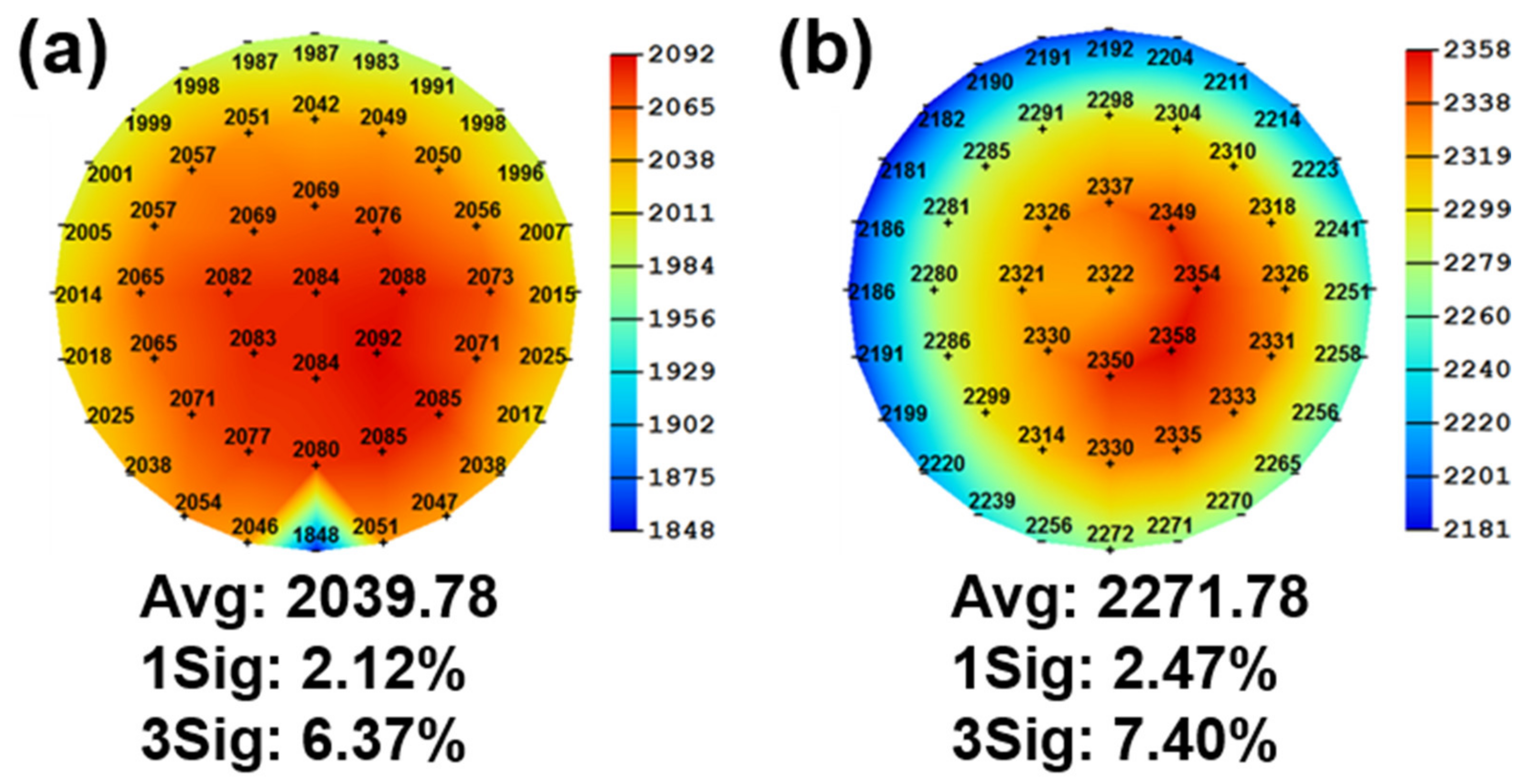
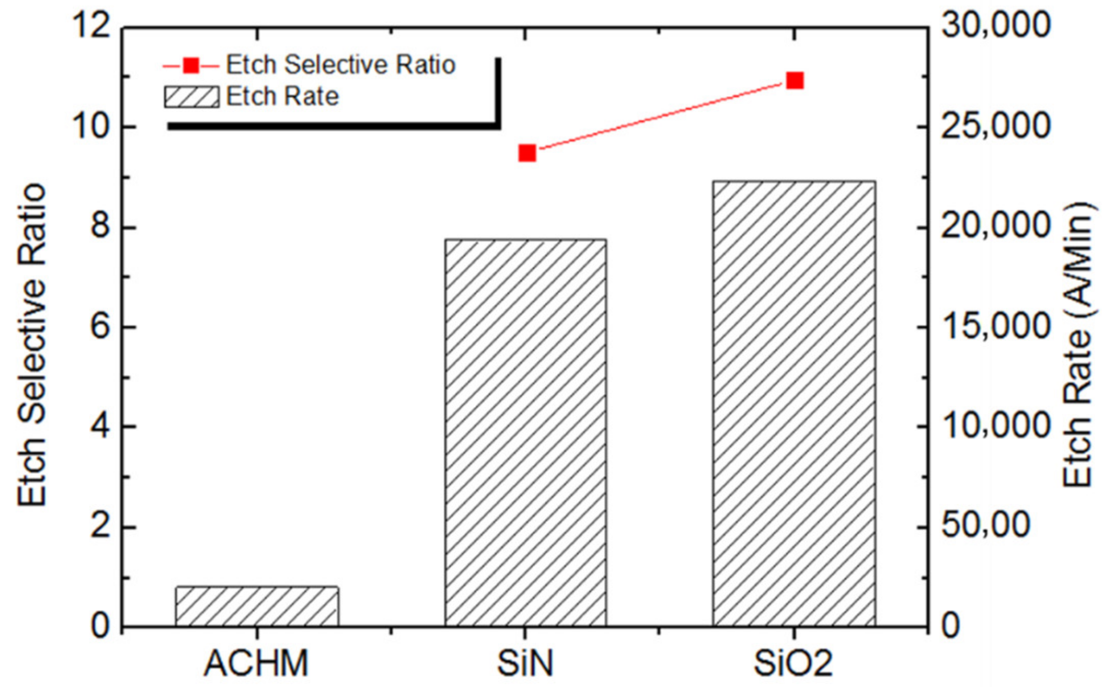
ACHM films (350 nm) were deposited on a p-type Si-substrate in a 300 mm standard PECVD system by using C2H2 and C3H6 as carbon sources. Wafers were cleaned in diluted HF and SC1 solutions in sequence. After cleaning, the wafer was loaded into the reactor with CCP (capacitive coupled plasma). RF power of 1000 W and a reactor pressure of 5 torr were used. The flow rates of C2H2 and C3H6 were both 1500 sccm. Different deposition temperatures of 300 °C, 350 °C and 400 °C were tested, and the deposition rate, film uniformity, extinction coefficient and dry etch rate were measured by a KLA-Tencor Aleris 8500 Spectroscopic Ellipsometry. Chemical structure and C–H bonding was measured by FTIR spectroscopy. The thickness of the film was measured at 49 different points selected from the 300 mm wafer. The deposition film was etched using O2 plasma and mixed CF4 and CHF3. The film thickness was measured after each deposition and etch process, and the dry etch selectivity was further calculated by TSiN/SiO2/TACHM, where TSiN/SiO2 and TACHM are the thickness of SiN or SiO2 and ACHM removed by chemical gas.

3. Results

Figure 1 shows the dependence of the deposition rate and non-uniformity on the deposition temperature by using C2H2 and C3H6 precursors. From Figure 1a, the deposition rate with C2H2 decreased from 6018 Å/min to 4941 Å/min when increasing the deposition temperature from 300 °C to 400 °C. Similar trend is observed for the test using C3H6 (decreased from 6081 Å/min to 5036 Å/min). Such dependence of the deposition rate on temperature is because of a lower incorporation of hydrocarbon reactants absorbed into the film at higher temperatures based on the absorbed layer model; the erosion process also became stronger at higher temperatures, leading to a lower deposition rate [20]. Figure 1b clearly suggests that the film non-uniformity is improved from 4.5% to 2.1% for C2H2, and from 3.5% to 1.96% for C3H6 when increasing temperature from 300 °C to 400 °C. This is also due to the lower incorporation of hydrocarbon reactants into film at elevated temperatures [21]. It should also be noted that increasing the substrate temperature is also beneficial to the compensation of the dangling bonds on the surface of the film, which further reduces the defects in the film and enhances the film density.
The extinction coefficient (EC) represents the capability of a chemical species or substance to absorb light at a particular wavelength. For HM applications, low EC values are typically required in 3D-NAND (<0.5 at 300 °C ~ 400 °C). Figure 2 shows the EC measured as a function of deposition temperature to study film optical characteristics. By increasing the temperature from 300 °C to 400 °C, the EC of ACHM film deposited with C2H2 was increased from 0.384 to 0.430 and the film using C3H6 was increased from 0.379 to 0.421. Such an increase in EC with increasing temperature is attributed to the increase of sp2 C–H bonds portion. According to the subplantation model, a higher temperature is favorable for the development of sp2 C–H bonds [22]. The sp2 chemical bonds are similar to graphite and can block more light.
It is known that there are three main absorption bands for ACHM film located at 2870 cm−1, 2930 cm−1, and 2955 cm−1, respectively. Hydrocarbons observed at 2870 cm−1 are attributed to the sp3–CH3 symmetric/C–H symmetric stretching mode. Hydrocarbons observed at 2930 cm−1 and 2955 cm−1 are ascribed to the sp3–CH2 and sp3–CH3 asymmetric C–H stretching mode, respectively. As shown in Figure 3, the absorption peak intensity of these bands decreases with increasing deposition temperature, but the curve profiles exhibit similar behavior. These spectra absorption results indicated that ACHM film has a lower content of C–H bonds at higher temperatures for both C2H2 and C3H6, which is due to the decrease of the sticking coefficient of hydrocarbon content, with an increase of deposition temperature [23]. By comparing the spectra obtained from the films using different precursors, the ACHM film using C2H2 illustrates relatively higher absorption intensity at all tested temperatures, which can be explained by the lower number of sp3–CH2 of the C2H2 film at 2930 cm−1 than that of the C3H6 film [24].
Figure 4 shows the dry etch rate of ACHM film as a function of deposition temperature. Lower etch rate is observed at a higher temperature for both films. Similarly, this is because of the lower incorporation of hydrocarbon and absorption reactants of atomic hydrogen in the surface at higher temperatures. More ions with sufficient energy will migrate resulting in a denser film, and thus a lower dry etch rate [25]. Figure 5a,b show the dry etch rate mapping at 400 °C of the film using C2H2 and C3H6, respectively. The 3-sigma value of etch rate with C3H6 was 6.37%, and the value was 7.40% with C2H2, which was slightly higher than C3H6. This suggests that ACHM with C3H6 had better uniformity and lower etch rate variation, which are critical factors considering practical applications in 3D-NAND fabrication process [19].
From the above results, higher temperatures will decrease the non-uniformity and etch rate, which were considered more important as a dry etch hard mask in 3D-NAND application due to the direct impact on yield data and process cost. Compared to C2H2, using C3H6 as a carbon source will increase the deposition rate from 4941 Å/min to 5036 Å/min, and decrease the non-uniformity from 2.1% to 1.96%. The dry etch rate is also decreased from 2271.78 Å/min to 2039.78 Å/min as shown in Figure 5. Although the EC is increased to 0.421 for the C3H6 precursor at a 400 °C deposition temperature, the value is sufficient for the requirement as a dry etch hard mask. It is easily concluded that the best condition for ACHM film processing with an optimized deposition rate, non-uniformity, EC and dry etch rate is by using C3H6 precursor and a 400 °C deposition temperature.
Finally, we compare the dry etch rates for SiN and SiO2 with ACHM by using a C3H6 precursor and a 400 °C deposition temperature for the purpose of verification of an effective etch hard mask. SiN and SiO2 are deposited at 400 °C by the same PECVD system. By calculating the dry etch selective ratio to SiN and SiO2 using the formular mentioned above, we have achieved the best dry etch selective ratio values of 10.9 and 9.5 for SiO2 and SiN at 90 W bias power and 0.125 torr pressure in the etch system (Figure 6). Such high etch selective ratios to SiN and SiO2 are very promising for practical application in 3D-NAND fabrication as dry etch hard masks. With the high etch selective ratio hard masks used in ploy gates and storage layers, it is possible to largely improve switching speed and storage intensity by scaling channel dimensions and increasing storage layers [26,27].

4. Conclusions

In summary, the deposition process and the ACHM film properties have been studied and compared by using different precursors in PECVD, and the deposition temperature is further optimized towards high-reliability film quality. The etch process and film properties are investigated, including the deposition temperature, film non-uniformity, etch rate and etch selective ratio to SiN and SiO2. A precursor/temperature co-optimization is developed which is effective in achieving sufficient etch selective ratio and film uniformity. Such process optimization can be very attractive in forming high-reliability ACHM in 3D-NAND fabrication process.

Author Contributions

Writing—Original Draft, Z.J.; Writing—Review & Editing, H.Z.; Supervision, Q.S. All authors have read and agreed to the published version of the manuscript.

Funding

This work was supported by the National Key Research and Development Program of China (2018YFB2202800), the Program of Shanghai Subject Chief Scientist (18XD1402800) and the Support Plans for the Youth Top-Notch Talents of China.

Data Availability Statement

The data presented in this study are available on request from the corresponding author.

Conflicts of Interest

The authors declare no conflict of interest.

References

  1. Park, S.H.; Kim, Y.; Kim, W.; Seo, J.Y.; Park, B.-G. Vertical-Channel STacked ARray (VCSTAR) for 3D NAND flash memory. Solid-State Electron. 2012, 78, 34–38. [Google Scholar] [CrossRef]
  2. Micheloni, R.; Crippa, L.; Zambelli, C.; Olivo, P. Architectural and Integration Options for 3D NAND Flash Memories. Computers 2017, 6, 27. [Google Scholar] [CrossRef]
  3. Kim, S.; Lee, S.H.; Park, S.K.; Kim, Y.; Cho, S.; Park, B.G. Investigation of Retention Characteristics Caused by Charge Loss for Charge Trap NAND Flash Memory. J. Semicond. Technol. Sci. 2017, 17, 584–590. [Google Scholar] [CrossRef]
  4. Pauliac-Vaujour, S.; Brianceau, P.; Comboroure, C.; Faynot, O. Improvement of high resolution lithography by using amorphous carbon hard mask. Microelectron. Eng. 2008, 85, 800–804. [Google Scholar] [CrossRef]
  5. Ho, C.Y.; Lin, X.J.; Chien, H.R.; Lien, C. High aspect ratio contact hole etching using relatively transparent amorpgous carbon hard mask deposition from propylene. Thin Solid Film. 2010, 518, 6076–6079. [Google Scholar] [CrossRef]
  6. Lai, C.C.; Chang, Y.H.; Chien, H.J.; Lu, M.C. Hard mask and lithographic capabilities improvement by amorphous carbon step coverage optimization in high aspect ratio device pattern. Vacuum 2018, 153, 267–273. [Google Scholar] [CrossRef]
  7. Lin, Y.-Y.; Chen, C.-C.; Li, C.-Y.; Wang, Z.-S.; Chen, C.-H. Pattern wiggling investigation of self-aligned double patterning for 2x nm node NAND Flash and beyond. In SPIE Advanced Lithography; SPIE: Washington, DC, USA, 2013. [Google Scholar]
  8. Yu, B.-L.; Huang, Y.; Luo, S.-A.; Cheng, Y.-S.; Hung, Y.-T.; Luoh, T.; Yang, L.-W.; Yang, T.; Chen, K.-C. APF Hard Mask Distortion Improvement for High Aspect Ratio Patterning; Institute of Electrical and Electronics Engineers (IEEE): New York, NY, USA, 2015; pp. 1–3. [Google Scholar]
  9. Negishi, N.; Takesue, H.; Sumiya, M.; Yoshida, T.; Momonoi, Y.; Izwa, M. Deposition control for reduction of 193 nm photoresist degradation in dielectric etching. J. Vac. Sci. Technol. B 2005, 23, 217–223. [Google Scholar] [CrossRef]
  10. Lee, S.; Jung, D.; Yang, J.; Boo, J.-H.; Kim, H.; Lee, J.; Chae, H. Characterization of oxygen and nitrogen rapid thermal annealing processes for ultra-low-k SiCOH films. J. Mater. Res. 2008, 23, 856–861. [Google Scholar] [CrossRef] [Green Version]
  11. Kaspar, P.; Jeyaram, Y.; Jäckel, H.; Foelske, A.; Kötz, R.; Bellini, S. Silicon nitride hardmask fabrication using cyclic CHF3-base reactive ion etching process for vertical profile nanostructure. J. Vaccum Sci. Technol. B 2010, 28, 1179–1186. [Google Scholar] [CrossRef]
  12. Liu, Z.; Shah, A.; Alasaarela, T.; Chekurov, N.; Savin, H.; Tittonen, I. Silicon dioxide mask by plasma enhanced atomic layer deposition in focused ion beam lithography. Nanotechnology 2017, 28, 085303. [Google Scholar] [CrossRef] [Green Version]
  13. Buijnsters, J.; Fernandez, R.G.; Jiménez, I.; Camero, M.; Agulló-Rueda, F.; Gómez-Aleixandre, C. Hydrogen quantification in hydrogenated amorphous carbon films by infrared, Raman, and x-ray absorption near edge spectroscopies. J. Appl. Phys. 2009, 105, 93510. [Google Scholar] [CrossRef] [Green Version]
  14. Ahmad, I.; Roy, S.; Rahman, A.; Okpalugo, T.; Maguire, P.; McLaughlin, J. Substrate effects on the microstructure of hydrogenated amorphous carbon films. Curr. Appl. Phys. 2009, 9, 937–942. [Google Scholar] [CrossRef]
  15. Durand-Drouhin, O.; Lejeune, M.; Benlahsen, M. Growth and bonding structure of hard hydrogenated amorphous carbon thin films deposited from an electron cyclotron resonance plasma. J. Appl. Phys. 2002, 91, 867. [Google Scholar] [CrossRef]
  16. Davis, C.A.; Knowles, M.; Amaratunga, G. Cross-sectional structure of tetrahedral amorphous carbon thin films. Surf. Coat. Technol 1995, 76, 316–321. [Google Scholar] [CrossRef]
  17. Kim, J.K.; Cho, S.I.; Kim, N.G.; Jhon, M.S.; Min, K.S.; Kim, C.K.; Yeom, G.Y. Study on the etching characteristics of amorphous carbon layer in oxygen plasma with carbonyl sulfide. J. Vac. Sci. Technol. A 2013, 31, 021301. [Google Scholar] [CrossRef] [Green Version]
  18. Lee, S.; Won, J.; Choi, J.; Park, J.; Jee, Y.; Lee, H.; Byun, D. Comparative study on the properties of amorphous carbon layers deposited from 1-hexene and propylene for dry etch hard mask application in semiconductor device manufacturing. Thin Solid Film. 2011, 519, 6683–6687. [Google Scholar] [CrossRef]
  19. Lee, S.; Won, J.; Choi, J.; Jang, S.; Jee, Y.; Lee, H.; Byun, D. Preparation and analysis of amorphous carbon films deposited from (C6H12)/Ar/He chemistry for application as the dry etch hard mask in the semiconductor manufacturing process. Thin Solid Film. 2011, 519, 6737–6740. [Google Scholar] [CrossRef]
  20. Piazza, F.; Grambole, D.; Schneider, D.; Casiraghi, C.; Ferrari, A.; Robertson, J. Protective diamond-like carbon coatings for future optical storage disks. Diam. Relat. Mater. 2005, 14, 994–999. [Google Scholar] [CrossRef]
  21. Von Keudell, A.; Jacob, W. Surface relaxation during plasma-enhanced chemical vapor deposition of hydrocarbon films, investigated by in situ ellipsometry. Appl. Phys. 1997, 81, 1531. [Google Scholar] [CrossRef]
  22. Hayashi, Y.; Hagimoto, K.; Ebisu, H.; Kalaga, M.K.; Soga, T.; Umeno, M.; Jimbo, T. Effect of Radio Frequency Power on the Properties of Hydrogenated Amorphous Carbon Films Grown by Radio Frequency Plasma-Enhanced Chemical Vapor Deposition. Jpn. J. Appl. Phys. 2000, 39, 4088–4093. [Google Scholar] [CrossRef]
  23. Von Keudell, A. Formation of polymer-like hydrocarbon films from radical beams of methyl and atomic hydrogen. Thin Solid Film. 2002, 402, 1–37. [Google Scholar] [CrossRef]
  24. Lai, C.C.; Chang, Y.H.; Chien, H.J.; Lu, M.C. Amorphous carbon process optimization to increase hard mask and lithographic capabilities by its step coverage improvement. In Proceedings of the 2017 6th International Symposium on Next Generation Electronics (ISNE), Keelung, Taiwan, 23–25 May 2017. [Google Scholar]
  25. Padhi, D.; Kim, B.H.; Witty, D. Dry etch selectivity of a-C:H hardmasks for sub-65 nm patterning applications. J. Vac. Sci. Technol. B Microelectron. Nanometer Struct. 2009, 27, 1809. [Google Scholar] [CrossRef]
  26. Regine, R. Non-equilibrium polaritonics - non-linear effects and optical switching. Ann. Phys. 2013, 525, 66–73. [Google Scholar]
  27. Lubatsch, A.; Frank, R. Behavior of Floquet Topological Quantum States in Optically Driven Semiconductors. Symmetry 2019, 11, 1246. [Google Scholar] [CrossRef] [Green Version]
Figure 1. The profile of (a) deposition rate and (b) non-uniformity with the increase of deposition temperature.
Electronics 10 01374 g001
Figure 2. The profile of the extinction coefficient as a function of deposition temperature.
Electronics 10 01374 g002
Figure 3. FTIR spectra of ACHM with different source of (a) C2H2 and (b) C3H6 at 300 °C, 350 °C and 400 °C.
Electronics 10 01374 g003
Figure 4. Dry etch rate as a function of deposition temperature.
Electronics 10 01374 g004
Figure 5. Dry etch rate map of the film using (a) C3H6 and (b) C2H2 at 400 °C.
Electronics 10 01374 g005
Figure 6. Etch Rate for ACHM, SiN and SiO2, and the etch selective ratio to SiN and SiO2 at 400 °C.
Electronics 10 01374 g006
Publisher’s Note: MDPI stays neutral with regard to jurisdictional claims in published maps and institutional affiliations.

