Article

Reducing Conducted Emissions at the Output of Full-Bridge DCDC Converters with High Voltage Steps

by
Pablo González-Vizuete
1,
Joaquín Bernal-Méndez
2,* and
María A. Martín-Prats
1
1
Department of Ingeniería Electrónica, Escuela Técnica Superior de Ingeniería, Universidad de Sevilla, 41092 Seville, Spain
2
Department of Física Aplicada III, Escuela Técnica Superior de Ingeniería, Universidad de Sevilla, 41092 Seville, Spain
*
Author to whom correspondence should be addressed.
Electronics 2021, 10(12), 1373; https://doi.org/10.3390/electronics10121373
Submission received: 5 May 2021 / Revised: 1 June 2021 / Accepted: 3 June 2021 / Published: 8 June 2021

Abstract

:
In this work, we analyze the impact of output filter design techniques aimed to reduce conducted emissions at the output of a DCDC power converter. A thorough analysis, based on high-frequency circuit models of the converter, is performed to assess expected improvements offered by different design strategies. This analysis is then confronted with measurements of conducted emissions at the output of a 300 W 48 V to 12 V Phase Shift Full Bridge (PSFB) prototype. Those experimental results demonstrate that a symmetric arrangement of the output LC filter and a direct bonding of the return output terminal of the converter to chassis are effective to reduce common mode conducted emissions at the output. Those results also demonstrate that the symmetry of the output LC filter can reduce conducted emissions in differential mode at high frequencies, where common mode to differential mode conversion is the predominant contribution to differential mode noise. However, direct bonding to chassis of the return output terminal may be ineffective at high frequencies due to the parasitic inductance associated with this connection. Main conclusions drawn for this analysis are applicable in general for isolated converters with a high voltage step between high and low voltage sides. Since the techniques of reduction of conducted emissions studied here do not increase the number of filter components, they are especially suitable for applications where high power density is an important requirement, e.g., aerospace or automotive applications.

1. Introduction

High efficiency and high power density are key requirements in power converters in several fields, such as automotive [1], aeronautics [2,3] and telecommunications [4]. In this context, current trends are aimed towards the use of higher switching frequencies and fast switches (e.g., wide bandgap semiconductor switches) to reduce volume and weight of passives without increasing converter switching losses [5]. However, rapid voltage and current changes associated with high switching frequencies increase electromagnetic compatibility (EMC) issues such as conducted and radiated emissions [6]. This makes it necessary to optimize the design of the converters to ensure compliance with mandatory EMC regulations while avoiding weight penalties associated with filtering requirements.
In general, techniques to reduce electromagnetic emissions of power converters fall either into strategies that inherently generate low noise [7,8], or techniques aimed to recirculate noise within the converter, thus keeping it away from the power leads [9]. A simple and effective design technique such as enforcing symmetry of the electromagnetic interference (EMI) filter at the input leads of the converter can be included within the latter category [10]. Furthermore, other passives such as transformers and inductors can be designed or arranged in a favorable manner in order to contain noise within the converter. For example, placement of equal inductors in both positive and return buses (symmetrical inductances), has already been implemented in an isolated boost converter [11] and a forward converter [12] as a strategy to reduce input filtering requirements. This same idea of splitting the inductance in two buses will be implemented at the output filter of an isolated converter in this work. Although we study a different topology and different measurement points for conducted emissions, [11,12] define a background for the filtering concepts that will be developed in this work. Similarly, effects of reduction of the equivalent noise sources at the input power leads of converters have been achieved by using current balancing techniques [11,13,14,15].
Valuable insights in common mode (CM) currents paths in isolated PSFB and resonant converters are provided in [13,16]. In those works, the transformer interwinding capacitances between the high voltage (HV) primary side and the grounded low voltage (LV) secondary side are identified as a main cause for common mode currents at the converter input leads. Nevertheless, no attention is paid to output conducted emissions. In [12], a reduction of the voltage difference in output terminals due to inductors symmetrization is reported in a forward converter, although the underlying mechanism of this phenomena is not thoroughly examined.
In general, the effect of techniques aimed to reduce conducted emissions of converters are analyzed solely at the input leads of the converter [10,11,12,13,14,16]. This is related to the fact that, in practice, most EMC regulations impose explicit limits to conducted emissions at the power leads (input) of the device under test (DUT). However, a power converter is a specific kind of DUT presenting output power leads, which can also become a source of conducted and radiated emissions that are able to cause EMI issues in nearby susceptible devices. This issue is also dealt with by EMC regulations [17,18]. For example, in the annex I of CISPR 25 [17], applicable to automotive equipment, measurement setups and limits of conducted and radiated emissions are defined for automotive devices with both high voltage (HV) and low voltage (LV) sources or loads, which is the case of DCDC converters. In that standard, conducted emissions at the LV power leads are limited. On the other hand, the aeronautical standard RTCA-DO-160 [18] establishes limits to conducted emissions on interconnecting bundles, which makes it necessary to control and limit conducted emissions at the output of DCDC converters. Moreover, this limitation in converter output conducted emissions is consistent with the susceptibility limits (RTCA-DO-160 Section 22) of a load device that is connected to the LVDC network generated by a DCDC converter. Finally, it is also worth pointing out that CM currents at the output power leads are the main source of radiated emissions [19]. Therefore, reducing CM conducted emissions at the output of the converter is a key technique to ensure compliance with limits imposed to radiated emission by the applicable EMC regulation.
This work analyzes the impact of several alternative configurations of the output LC filter on output CM and differential mode (DM) conducted emissions of an isolated PSFB converter. In particular, the effect of both symmetrization of the output filter inductors and direct connection to chassis of the return output terminal of the converter are thoroughly studied and measured. We demonstrate that the configuration of the output filter of this converter can be optimized to reduce CM emissions with no significant penalty in terms of weight or volume of the converter. Furthermore, we show that DM emissions can be reduced by proper mitigation of CM to DM conversion. The output filter design techniques discussed here are especially interesting in applications with a high voltage step between the isolated HV input and LV output, where relatively high CM currents flow from the HVDC side to the LV side through the transformer parasitic capacitances [20].
This manuscript is organized as follows. In Section 2, the noise sources of the PSFB converter are presented, as well as a generic equivalent Thèvenin model of the converter at the output LC filter. The qualitative impact of the proposed LC filter configurations on output CM and DM conducted emissions will also be discussed. Section 3 describes the setup and measurement method used to obtain the measured conducted emissions presented in Section 4. Measurements have been performed for the different filter configurations in an isolated 48 V to 12 V PSFB prototype. The main conclusions of this work are summarized in Section 5. Finally, details about the characterization of the components of the measured converter with most impact in output conducted emissions are given in Appendix A.

2. Analysis

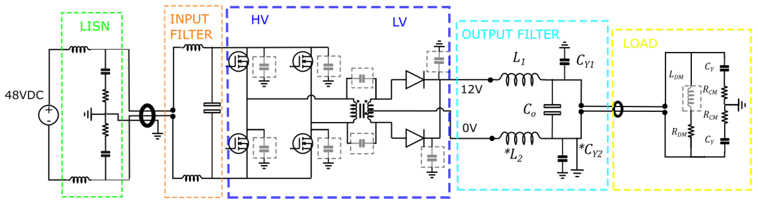
2.1. Topology of the DCDC Power Converter and Noise Sources

The PSFB is a suitable topology for isolated and unidirectional power transfer in mid power applications, in the range of units of kilowatts [21,22,23]. This topology, shown in Figure 1, features a controlled full bridge in the HV side, which generates an AC voltage at its output at the switching frequency. The high frequency transformer is used to reduce the AC voltage between HV and LV sides and to provide galvanic isolation. A center-tapped transformer enables the use of only two switches to rectify the AC output of the transformer. The DC component of the rectifier output is filtered by an output LC filter.
The Line Impedance Stabilization Networks (LISN) in Figure 1 is intended for measuring conducted emissions of the converter at its input leads [18,24]. A LISN offers a controlled impedance to the noise sources of the converter, thus ensuring repeatable measurements. Depending on the particular standard, a LISN might also be required at the output leads [17], or the load impedance should be similar to that found in the real device operation [18]. In the measurement setup in Figure 1, AC coupled resistors to ground ( R C M and C y ) have been included to ensure a repeatable measurement of noise at the output terminals of the converter. In that schematic, R D M and L D M account for the resistive and inductive parts of the impedance of the load.
The goal of this work is to study and compare the impact of different output LC filter configurations on noise currents flowing to the load. In particular, we are interested in limiting CM noise currents because they can easily compromise compliance of the converter with EMC regulations [19,25]. In PSFB and similar isolated topologies, CM noise in the LV side is greatly determined by HV switching operation, switches parasitic capacitances to ground, transformer parasitic interwinding capacitances, and output terminals filtering to ground/chassis [13,16,26]. In Figure 1, parasitic capacitances that offer paths for CM currents have been encircled by dashed lines.
Under the presence of such CM perturbations in the LV side, the output LC filter must be optimized to reduce output CM emissions and also to mitigate CM to DM conversion that could lead to undesirable DM conducted emissions. In order to reduce CM currents flowing to the load, it is usual to connect capacitors between the output terminals and the chassis ( C y 1 and C y 2 in Figure 1) or to make a direct chassis ground connection of the return terminal (if allowed by specifications). In this work, we study and compare the impact on noise emissions of both configurations. For the sake of conciseness, the configuration with a high frequency (HF) capacitor between each bus and the chassis will be referred to as ‘CC’, whereas the configuration in which the return output terminal is directly connected to chassis will be referred to as ‘C0VG’. Furthermore, we will study the effect on noise emissions of increasing symmetry of the output LC filter. With this aim, we will compare an asymmetric case (denoted as ‘AS’), where the whole inductance of the LC output filter is in the positive bus ( L 1 = L , L 2 = 0 in Figure 1), with a symmetric case (referred to as ‘S’) where the same inductance is split into two equal inductances in the ‘12 V’ and the ‘0 V’ buses ( L 1 = L 2 = L / 2 in Figure 1).

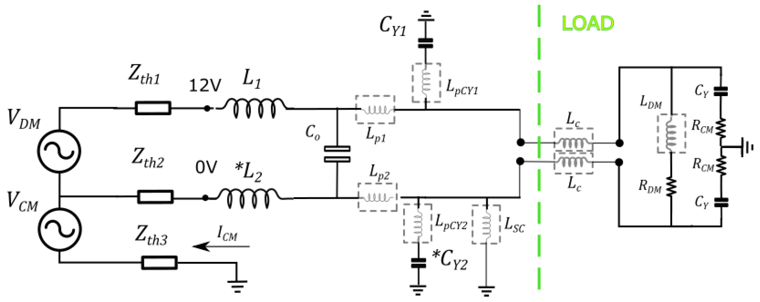
2.2. HF Model of the Converter at the Output

In order to facilitate the analysis of the effect of the output filter on noise flowing to the load, in Figure 2 the converter is replaced by its equivalent model. This model includes two frequency-dependent voltage sources ( V C M and V D M ), and also three frequency-dependent source impedances ( Z t h 1 , Z t h 2 and Z t h 3 ) [27]. The CM source, V C M , is related to switched voltages, (especially HV side MOSFETs), and Z t h 3 is closely related to the impedances seen by CM currents when flowing between the HV side and LV side, thus transformer interwinding capacitance greatly determines this impedance [20]. In general, obtaining the exact frequency-dependent parameters of the model in Figure 2 is not easy [28,29]. Nevertheless, this model simplifies the analysis of the impact of the different filter configurations in the conducted emissions at the output terminals of the converter.
The circuit model in Figure 2 includes all the output filter and load impedances, including some parasitic inductances that were not represented in Figure 1, but that play an important role in conducted emissions at high frequencies. In particular, L p 1 and L p 2 model the parasitic inductance of leads connecting power printed circuit board (PCB) and the converter output connectors. L p C Y 1 and L p C Y 2 model the parasitic equivalent series inductance (ESL) of C y 1 and C y 2 , respectively, including the inductance associated with the bonding to the grounded chassis. In the ‘C0VG’ configuration, L S C models the parasitic inductance of the bonding of the output terminal to the chassis. The L c inductances account for the parasitic inductances of the output power leads connecting the output of the converter to the load.

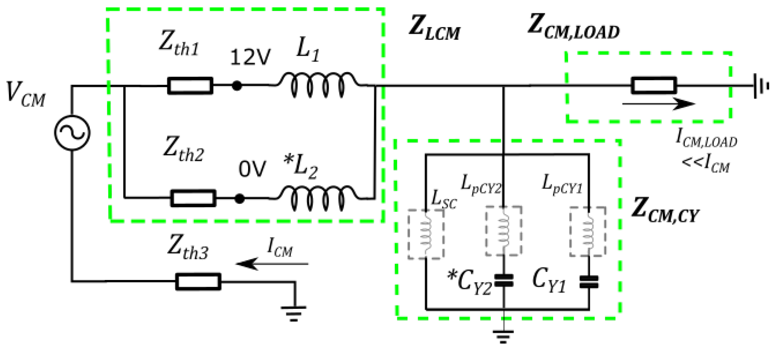
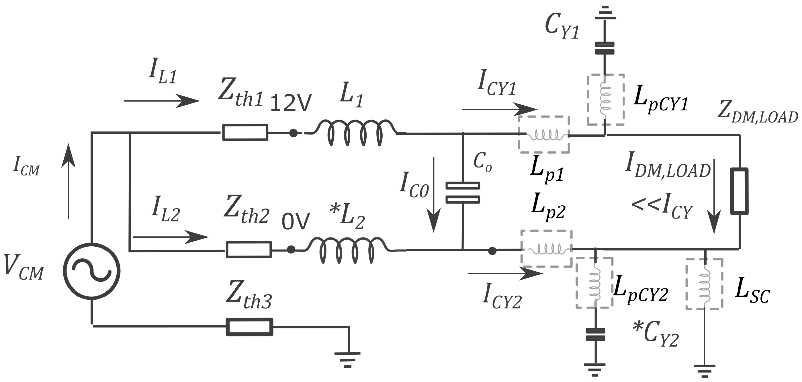
2.3. CM Conducted Emissions

In order to qualitatively understand the filter impact on CM output currents, the circuit model in Figure 2 can be further simplified as shown in Figure 3. This simplified circuit model is valid for all filter configurations with a caveat for the ‘C0VG’ configuration at high frequencies which will be addressed later. It is important to point out that the simplified circuit model in Figure 3 has the purpose of making the undelaying CM filtering mechanisms more evident that the complete model in Figure 2.
Two key assumptions have been made to get to the simplified model in Figure 3 from that in Figure 2:
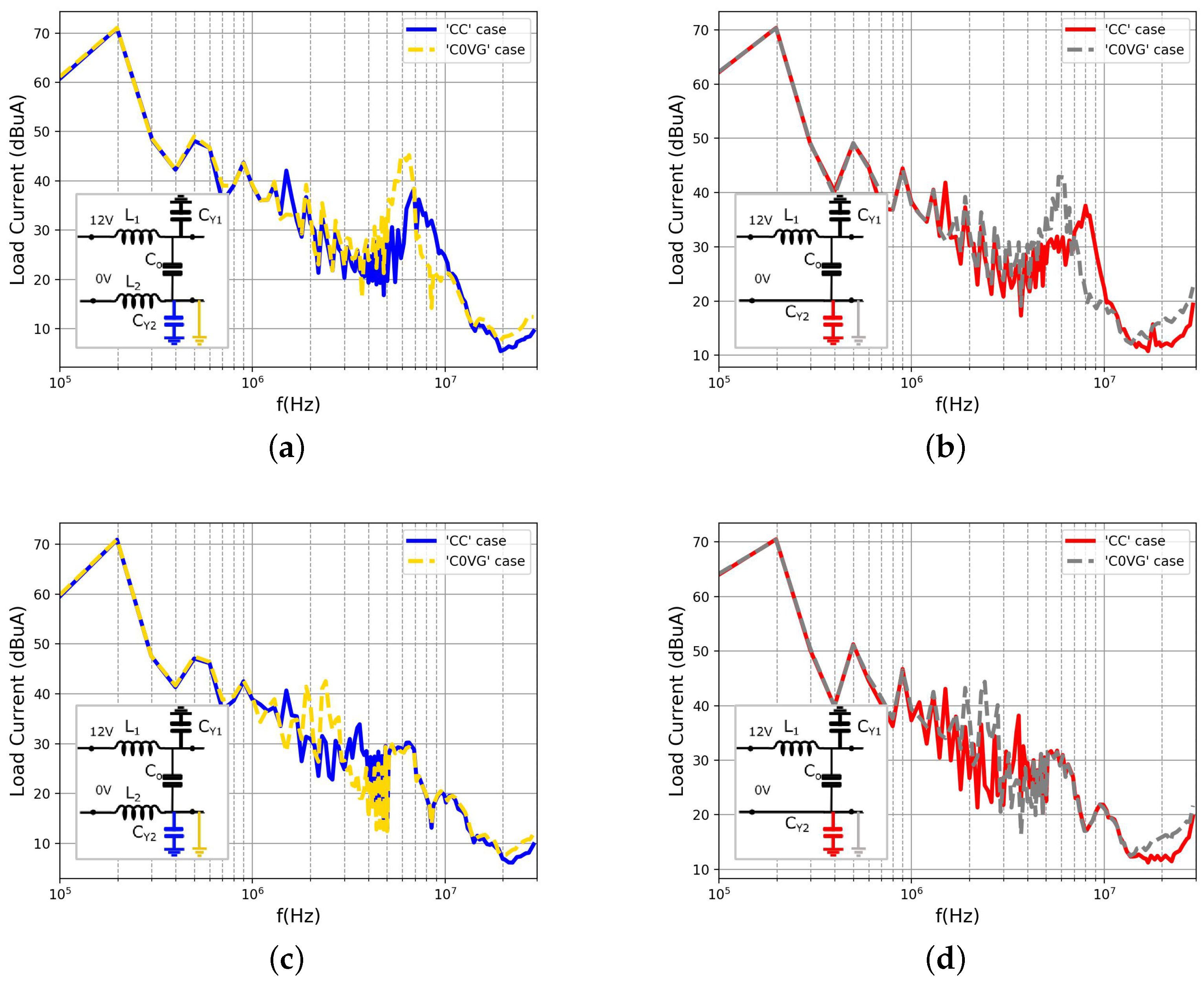
  • The impedance of the array of capacitors that conform C o is typically much lower than that of C y at low frequencies, and those of the parasitic inductances L p 1 , L p 2 , L p C Y 1 , L p C Y 2 and L S C at high frequencies. Therefore, this array of capacitors can be regarded as a short circuit.
  • The impedance of Z t h , 3 in series with both Z ( L 1 ) + Z t h , 1 and Z ( L 2 ) + Z t h , 2 is much larger than the rest of impedances of the filter. This assumption, together with the fact that voltage drops in L p 1 and L p 2 are expected to be roughly the same in ‘CC’, allows us to neglect the effect of L p 1 and L p 2 . Note that at low frequencies at which L p 1 and L p 2 can be ignored, the model in Figure 3 is also valid for both ‘CC’ and ‘C0VG’ cases.
The impedances in this simplified model are grouped in Figure 3 into four key impedances: one is Z t h 3 , another one is given by Z L C M , which accounts for the contribution of Z t h 1 , Z t h 2 , Z ( L 1 ) and Z ( L 2 ) . A third impedance, denoted as Z C M , C Y in Figure 3, is the contribution of the impedances associated with the capacitances or the direct connection between the power leads and the grounded chassis. Furthermore, Z C M , L O A D in Figure 3 stands for the impedance to ground seen at the load of the converter by the CM currents. Note that, since the C Y capacitors are expected to divert most of the CM current back to the chassis, the current I C M , L O A D flowing towards the load impedance should be much lower than the net CM current I C M .
The circuit model in Figure 3 shows that, in general, CM conducted emissions at the output of the converter can be reduced by increasing Z L C M . Therefore, it is interesting to estimate Z L C M for the different filter configurations. For the ‘AS’ case, Z L C M can be obtained as:
Z L C M , A S = ( Z t h 1 + j 2 π f L ) Z t h 2 Z t h 1 + j 2 π f L + Z t h 2 { 2 π f L > > Z t h 1 , Z t h 2 } Z t h 2
In the ‘S’ case, Z L C M can be calculated as:
Z L C M , S = ( Z t h 1 + j 2 π f L / 2 ) ( Z t h 2 + j 2 π f L / 2 ) ( Z t h 1 + j 2 π f L / 2 ) + ( Z t h 2 + j 2 π f L / 2 ) { 2 π f L > > Z t h 1 , Z t h 2 } j 2 π f L / 4
where in (1) and (2) it is assumed that | Z ( L ) | = | 2 π f L | | Z t h 1 | , | Z t h 2 | . Considering that at the frequencies of interest Z ( L ) is quite large, this must be true for typical values of Z t h 1 and Z t h 2 . From (1) and (2), it can be inferred that | Z L C M , A S | | Z L C M , S | . Consequently, the ‘AS’ case should give rise to higher CM conducted emissions ( I C M , L O A D ) at the output of the converter, regardless of the grounding configuration of the output terminals.
To analyze the effect on CM noise emissions of the converter of the two strategies considered for connection of the output terminal to chassis (‘CC’ and ‘C0VG’), it is also useful to examine the circuit model in Figure 3. In this circuit model, it can be seen that the main difference between ‘CC’ and ‘C0VG’ configurations is that they lead to different values of Z C M , C Y . In fact, Z C M , C Y in ‘C0VG’ is determined by the parasitic L S C , and therefore it is expected to be lower than Z C M , C Y in ‘CC’, which is given instead by the parallel impedance of both C y capacitors. Therefore, assuming that the total CM current I C M is approximately the same for the ‘C0VG’ and the ‘CC’ configurations, this makes the ‘C0VG’ configuration preferable to the ‘CC’ connection for reduction of CM conducted emissions. The assumption that I C M is approximately the same for the ‘C0VG’ and the ‘CC’ configurations can be justified by noting that I C M is mostly determined by Z t h 3 and Z L C M because Z t h 3 is a high impedance. Therefore, Z t h 3 + Z L C M will be typically much greater than the rest of the impedances in Figure 3. In other words, V C M along with Z t h 3 + Z L C M behaves as a current source feeding the parallel connection of Z C M , C Y and Z C M , L O A D . Since this current is split into I C M , L O A D and the current diverted to the chassis through Z C M , C Y , it can be readily concluded that a lower Z C M , C Y will reduce I C M , L O A D . However, a caveat should be added with respect to the validity of the circuit model in Figure 3. As earlier pointed out, this simplified model is not strictly correct for the ’C0VG’ case at high frequencies, because neglecting the parasitic L p 1 and L p 2 inductances in Figure 2 does not seem justified in that case. Nevertheless, and despite the fact that a rigorous analysis is more cumbersome in that particular case, it can be demonstrated that a lower Z C M , C Y should also reduce CM emissions in that case.
Summing up, CM conducted emissions are expected to be reduced by a parallel arrangement of the inductances of the output filter (‘S’ configuration) because this configuration increases the impedance seen by the CM currents. Furthermore, a direct bonding to chassis of the ‘0V’ power lead (‘C0VG’ configuration) is also expected to reduce CM conducted emissions of the converter by allowing internal recirculation of CM currents.
Finally, it is interesting to note that the difference between the performances at filtering CM noise emissions of ‘C0VG’ and ‘CC’ configurations should be higher at low frequencies, where the impedance of C y is capacitive and much greater than that of L S C . In this frequency region, this difference should increase with decreasing frequency and for smaller C y .

2.4. DM Conducted Emissions

Conducted emissions in DM are determined both by DM noise sources and also by CM to DM conversion [10]. This mode conversion is expected to be especially relevant in DCDC converters with a high voltage step (hence a significant CM noise source at the primary) and transformers with large interwinding capacitances (e.g., planar transformers [30]).
Since the grounding configuration has little effect on DM noise currents flowing at the output of the converter, any measurable effect caused on DM conducted emissions by changes on output filter and/or grounding configurations should be accounted for by the effect of the filter and/or grounding on CM/DM conversion.
To analyze the mechanism of CM/DM conversion and its impact on the different filter configurations studied here, Figure 4 represents the general circuit model at the output filter under a CM excitation. In that figure, the CM current entering the output filter, I C M , is split into currents I L 1 and I L 2 , flowing through L 1 and L 2 , respectively. Furthermore, in Figure 4, I C Y 1 and I C Y 2 represent currents that flow to ground through C Y 1 and C Y 2 (or the short circuit in ‘C0VG’), respectively. Current I C 0 flows through C 0 , due to an impedance unbalance in the filter. Furthermore, a current I D M , L O A D can flow to the DM load ( Z D M , L O A D ) due to CM to DM mode conversion, as we will discuss. Note that since Z D M , L O A D is typically much larger than the output impedance of the converter at the frequencies of interest, conducted emissions are expected to be mostly contained within the converter.
We will first study CM/DM conversion for each filter and grounding configuration at low frequencies (i.e., typically from a hundred kHz to units of MHz), where parasitic inductances can be neglected in the circuit model in Figure 4. First, we will focus on the ‘S’ cases. As discussed in Section 2.3, in ‘S’ cases, I C M is expected to be smaller than in ‘AS’ cases. Moreover, in ‘S’ cases, I C M is expected to be equally split into the L 1 and L 2 branches in Figure 4, i.e., I L 1 I L 2 . In the particular case of the ‘S,CC’ configuration, those equal currents see the same impedance to ground. Therefore, a very low CM/DM conversion is expected. On the other hand, in ‘S,C0VG’, I L 2 flows to ground through the ground bonding ( L S C ), whereas most of I L 1 (≃ I C M / 2 ) will flow to ground through the low impedance offered by C 0 . Therefore, a certain CM/DM conversion should be expected. For the ‘AS’ cases, I C M will mostly flow through the ‘0V’ bus, i.e., I L 2 I C M I C Y 2 . In ‘AS,C0VG’, I C Y 2 finds a very low impedance path to ground, whereas I L 1 I C 0 I C M . Therefore, a low CM to DM conversion is expected for the ‘AS,C0VG’ configuration at low frequencies. By contrast, for the ‘AS,CC’ case, the presence of the C Y 2 capacitors means that the relatively large CM current I L 2 I C M is not so efficiently diverted to ground at low frequencies. Instead, I L 2 finds a current divider with similar impedances through C Y 2 and the series impedance of C Y 1 and C 0 . Therefore CM/DM conversion is expected to be more significant in this case compared with the ‘AS,C0VG’ case. Table 1 summarizes the main conclusions obtained in this discussion. Since the effect of parasitic inductances has not been considered in the above discussion, those conclusions are expected to remain valid as long as frequencies are sufficiently low as to make negligible the effect of parasitic inductances.
It is interesting to analyze whether the above conclusions must be modified at high frequencies. At high frequencies (i.e., tens of MHz), parasitic impedances at the output play an essential role in CM to DM conversion, which is expected to modify the qualitative analysis performed for low frequencies. In fact, in this scenario, DM current I D M , L O A D is given by the expression:
I D M , L O A D = I C 0 Z C 0 + 2 π f j L p ( I C Y 2 I C Y 1 ) Z D M , L O A D
where Z C 0 stands for the impedance of C 0 . Furthermore, in (3) a symmetrical layout is assumed. Therefore, the parasitic inductances of the traces of the PCB connecting the LC output filter to the output connectors of the converter are assumed to be equal, i.e., L p 1 = L p 2 = L p . The simplified expression (3) helps to clarify the CM to DM conversion mechanism, which is difficult to be ascertained from a direct analysis of the model in Figure 2.
Equation (3) shows that at high frequencies, DM conducted emissions are greatly determined by parasitics, which depend on the particular implementation (layout) of the converter. This makes it difficult to obtain general conclusions regarding DM conducted emissions. However, we can focus on a representative case in which Z C 0 impedance is smaller than the impedances of L p , L p C Y 1 and L p C Y 2 . This is to be expected because Z C 0 is a capacitive impedance, which is usually implemented by an array of capacitors in parallel (hence with low parasitic inductance). We will also assume that L p C Y 1 = L p C Y 2 , which is the case of a symmetrical layout. Finally, it is reasonable to assume that the bonding to chassis of the return lead has been carefully implemented in such a way that the inductance of the bonding to ground, L S C , is smaller than L p C Y 1 . Under these assumptions, the main conclusions obtained at low frequencies regarding CM to DM conversion for the ‘CC’ configurations remain unaltered at high frequencies. However, an exception occurs in the ‘C0VG’ cases. In the ‘S,COVG’ case, a slight difference between low and high frequencies comes from the fact that a part of I L 1 is also expected to flow through C 0 , but a non-negligible I C Y 1 is also expected. The reason is that, as frequency increases, the ratio between the impedance of the short circuit bonding path and the C Y 1 path increases from 0 to a certain value less than a half, which depends on the parasitic inductance values. For this same reason, conclusions greatly change at high frequencies in ‘AS,C0VG’: the large current I C M I L 2 (much larger than in ‘S’) partly flows through L p 2 and L S C , but a non negligible part of this large current also flows through C 0 , L p 1 and L p C Y 2 . In short, the ‘AS,C0VG’ filter configuration is expected to lead to a high CM to DM conversion, but only at high frequencies due to the effect of parasitic inductances. Predicted currents associated with CM/DM conversion at high frequencies have been summarized in Table 2.

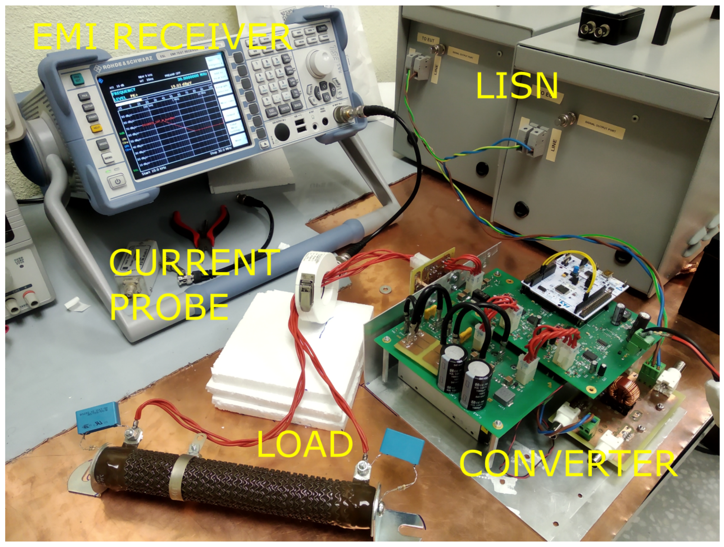
3. Materials and Methods

In order to validate the predicted behavior of the studied output filter configurations, we have measured both DM and CM currents at the output of a 300 W PSFB converter prototype between 100 kHz and 30 MHz, which is a frequency range where EMC standards typically limit conducted emissions [17,18,24]. To measure noise currents we have used a clamp-on broadband current probe (BCP-512 of AH-Systems). A picture of the measurement setup is shown Figure 5. This setup has the same structure as the schematic in Figure 1. Namely, the converter is connected to the DC source through a LISN and the output load is a resistor between output terminals. Furthermore, a RC network is connecting each load terminal to the ground copper plane. In Figure 5, we can also see the current probe at the output leads. Such a current probe is connected to the EMI receiver, and it can be conveniently clamped to measure either CM or DM currents.
Table 3 shows the parameters of the circuit model of the output leads of the converter (Figure 2) obtained for this measurement setup by following the approach described in Appendix A. This characterization of the measurement setup has allowed us to verify that the key assumptions made in our analysis about typical expected values of impedances are in concordance with measurement conditions determined by the measurement setup. For the sake of clarity, some parasitic capacitances C p or parasitic resistances R p that have been included in Table 3 have been omitted in Figure 2, Figure 3 and Figure 4 when not relevant to the discussion.

4. Results

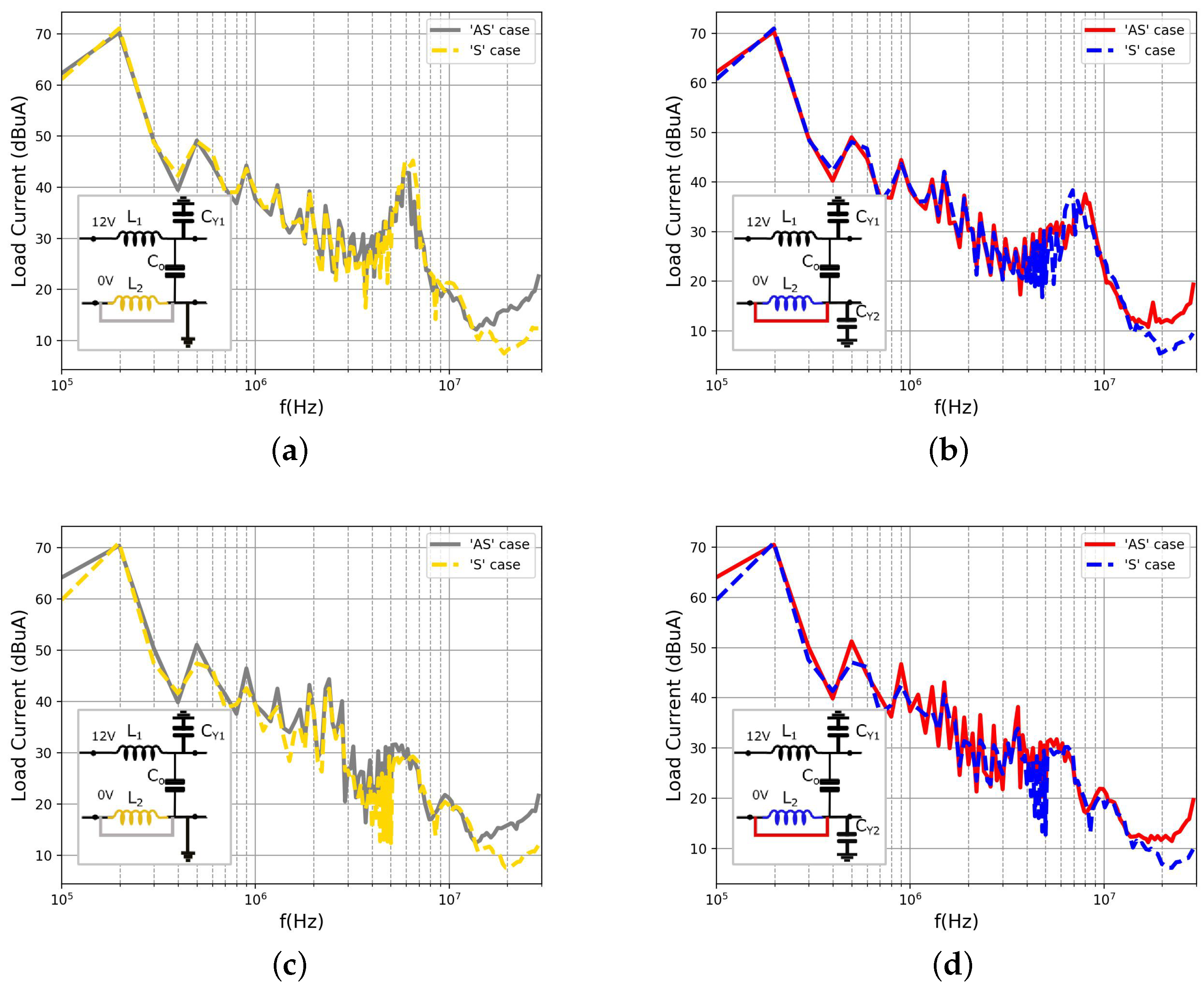
4.1. CM Conducted Emissions at the Output of the Converter

In this section, we analyze the effect of output filter symmetry on the emission of CM currents at the output leads of the converter. In the graphs in Figure 6, we compare the performance of a filter with a symmetric configuration of the inductors (‘S’ case) with the asymmetric or ‘AS’ case. In particular, in Figure 6a, we carry out the comparison when one of the output terminals is connected to the ground and a 10 nF C y capacitor is placed in the other terminal (‘C0VG’ case). The same comparison is presented in Figure 6b for the ’CC’ case: two 10 nF C y capacitors connected to each output terminal. Figure 6c,d represent the same cases than in Figure 6a,b, but 50 nF C y capacitors are used instead.
These results reveal that the ‘S’ configuration yields a reduction of CM currents of roughly 8 dB in the 10 MHz–30 MHz frequency range, regardless of C y value or configuration. In the mid frequency range from 2 MHz to 5 MHz, CM output currents are also lower in general for ‘S’, with a maximum reduction of 10 dB for the ‘CC’ case with C y = 10 nF (Figure 6b).
It can be observed in Figure 6 that in all the cases, the CM output currents present a peak between 4 MHz and 7 MHz, which is more pronounced in the ‘S’ case. We have checked that capacitors C y are involved in this CM peak and that damping resistors of 1.5 Ω reduce those peaks in approximately 10 dB without significantly altering the rest of the curve (results not shown).
In general, we can conclude from results in Figure 6 that the symmetrization of the output inductors in the two buses contributes to an overall reduction of CM currents in the output power leads, especially in the high frequency range (10 MHz to 30 MHz). These experimental results are consistent with the conclusions of the analysis presented in Section 2.
To facilitate the analysis of the effect on CM noise of the configuration of the C y capacitors, in Figure 7 we have rearranged the results in Figure 6 in such a way that in each plot, ‘CC’ and ‘C0VG’ cases are compared for the same configuration of the output inductors. Therefore, in Figure 7a, we compare ‘CC’ and ‘C0VG’ for the ‘S’ case, whereas in Figure 7b, we compare ‘CC’ and ‘C0VG’ for the ‘AS’ case. In both plots with C y = 10 nF. In Figure 7c,d, the same comparisons are performed for C y = 50 nF. The results shown in Figure 7 reveal that, when compared with the ‘C0VG’ alternative, the symmetric ‘CC’ configuration of the C y capacitors gives rise in general to higher emissions of CM currents at mid and high frequencies. The analysis presented in Section 2.3 anticipates this result as a consequence of the low impedance path that the direct bonding to ground employed in the ‘C0VG’ case offers to noise currents. An additional support to this argument is provided by the fact that the difference between ‘CC’ and ‘C0VG’ cases is reduced as C y capacitance increases, as it can be observed in the curves in Figure 7. This is especially true at frequencies below 10 MHz because at those relatively low frequencies, the effect of parasitic inductances on impedances to ground can be neglected. At high frequencies (above 10 MHz), ‘C0VG’ also exhibits lower output CM currents than ‘CC’, but this difference has a much weaker dependence with the value of the C y capacitance, since at these frequencies, the impedances to ground are mainly determined by parasitic inductances. As an additional remark, it is interesting to note that at 100 kHz, ‘CC’ outperforms ‘C0VG’ by 5–10 dBuA. However, this is most probably associated with a resonance at that frequency, which does not affect the general conclusions of this work.
The results presented in this section allow us to conclude that symmetry of the inductors of the output LC filter and a ‘C0VG’ bonding scheme reduce CM conducted emissions. However, note that a direct bonding of the ‘0V’ output terminal to ground might not be possible in some particular cases due to isolation requirements of the converter.

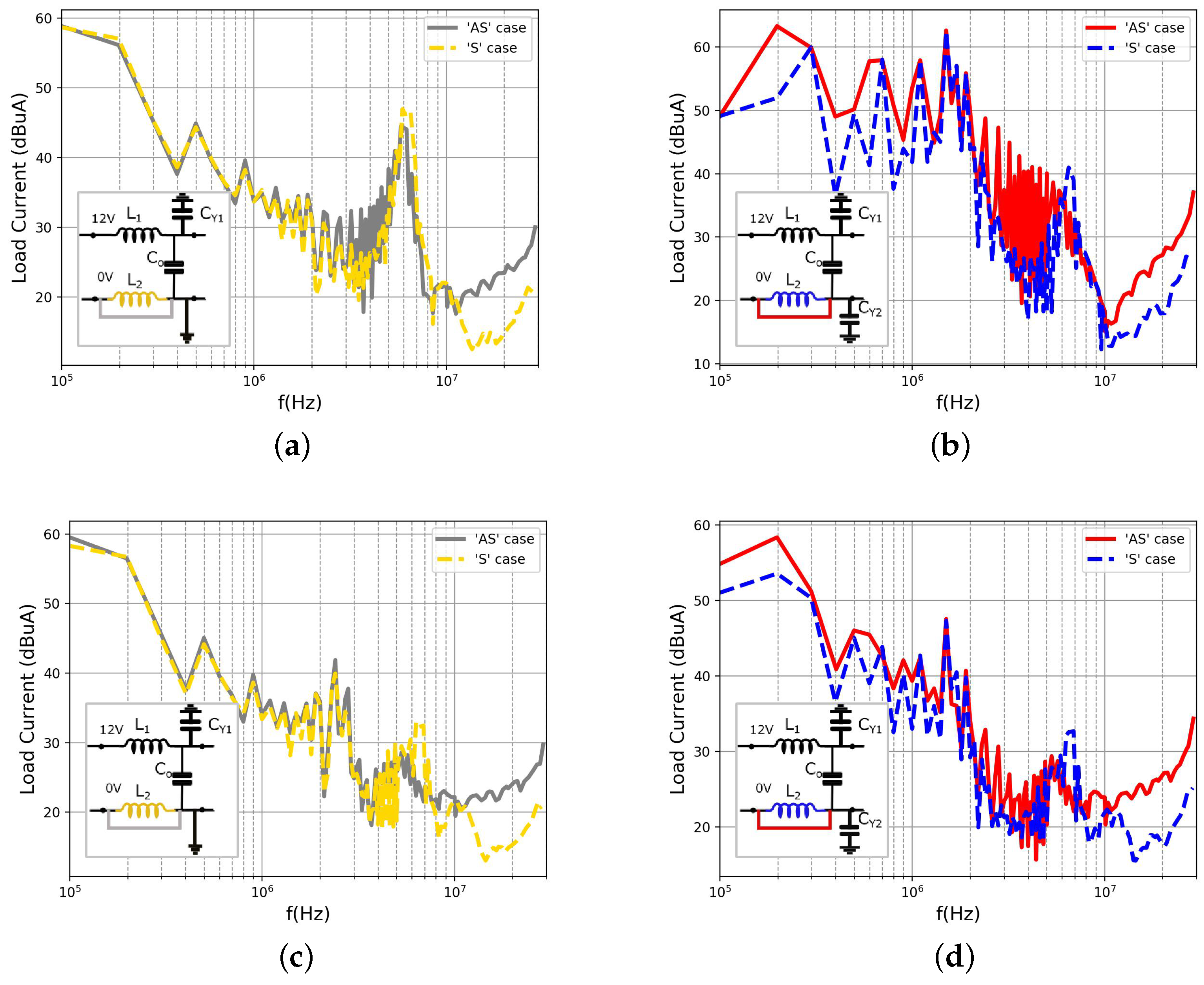
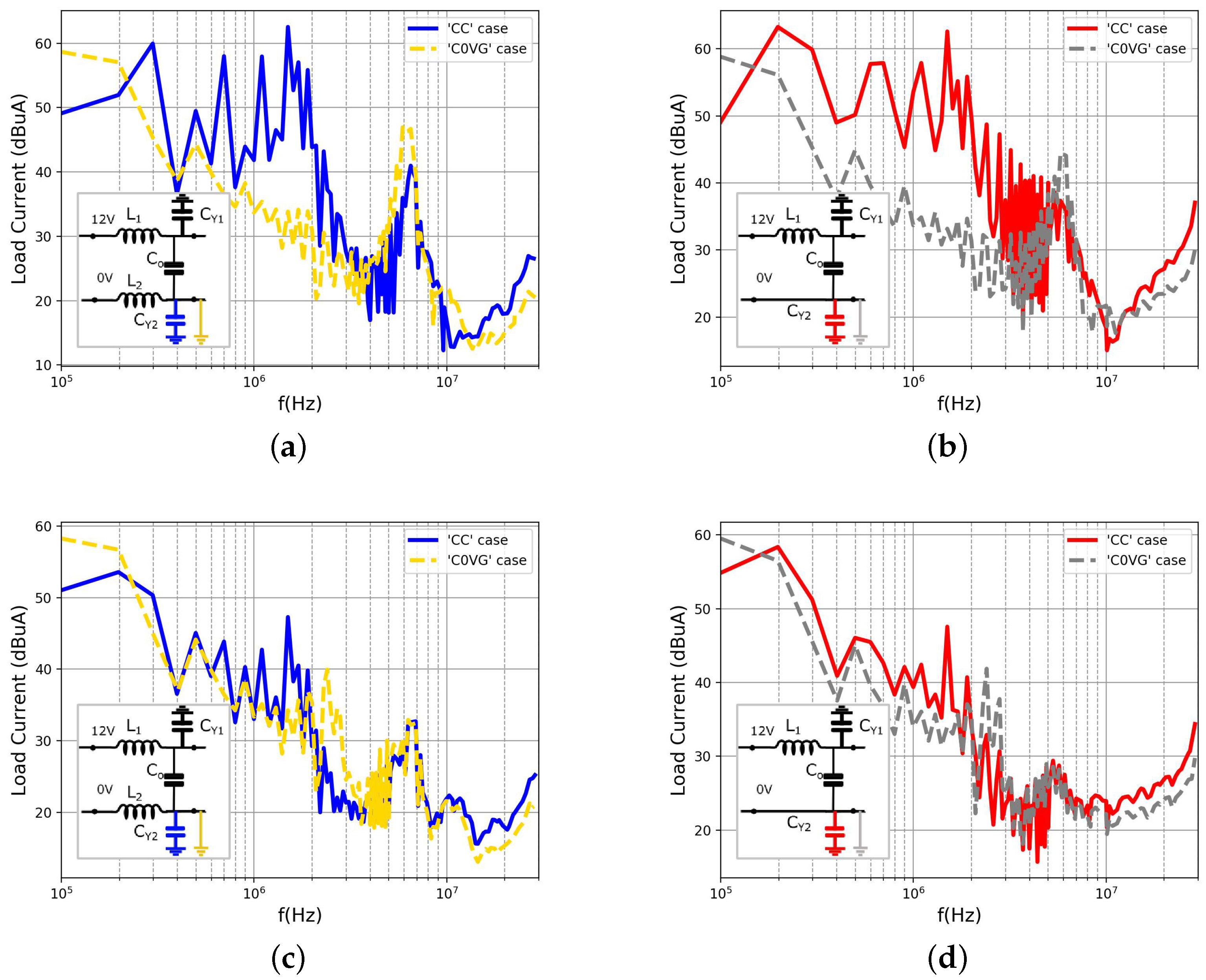
4.2. DM Conducted Emissions at the Output of the Converter

Regarding DM conducted emissions, the analysis presented in Section 2.4 and summarized in Table 1 indicates that symmetry of the inductors of the LC output filter should reduce in general CM to DM conversion, although the ‘AS,C0VG’ case could be advantageous at low frequencies. In order to verify these theoretical conclusions, in the plots in Figure 8, we have compared the measured output DM currents for the ‘S’ and ‘AS’ cases. This has been done for the ‘C0VG’ and the ‘CC’ configurations, respectively, in Figure 8a,b for C y = 10 nF. In Figure 8c,d, the same comparisons are presented for C y = 50 nF.
Results in Figure 8 reveal that ‘S’ filters outperform ‘AS’ filters, especially in the high frequency range of 15 MHz to 30 MHz. In fact, at 30 MHz the difference reaches 10 dB regardless of the grounding configuration or C y value. In contrast, at mid frequencies, from 1 MHz to 15 MHz, the differences are almost negligible. Results for C y = 50 nF (see Figure 8c,d) show slight improvements of up to 4 dB provided by the ‘S’ case with respect to the ‘AS’ case.
In order to analyze the effect of the C y configuration in the DM output currents, in Figure 9 we have rearranged the measurements presented in Figure 8, so that ‘CC’ and ‘C0VG’ cases are represented in the same plot for the sake of comparison. In all the comparative measurements shown in Figure 9, we can observe that DM noise current emissions are very similar for the ‘CC’ and ‘C0VG’ cases. In fact, only the resonance around 6MHz changes to a higher frequency for ‘CC’ with respect to the ‘C0VG’ case. Furthermore, ‘CC’ case offers a slight improvement (≃4 dB) with respect to the ‘C0VG’ case for frequencies above 15 MHz.
Summing up, results in this section confirm that a reduction of DM emissions thorough adequate output filter arrangement can only be achieved at frequencies where CM/DM conversion is the predominant source of DM emissions. In this case, this occurs at high frequencies. For this reason, a symmetric arrangement of the output filter inductances (‘S’ case) offers some advantages above 15MHZ. By contrast, a ‘C0VG’ scheme has a slight negative impact in DM emissions at high frequencies. As discussed in Section 2.4, the effect of parasitic inductances, which are highly dependant on the particular layout, accounts for this decline of the performance of the ‘C0VG’ configuration at high frequencies.

5. Discussion

This work analyzes and quantifies reduction on conducted CM and DM emissions at the output power leads of a power converter achieved by design techniques based upon symmetric/asymmetric placement of components of the output filter of the converter. These design techniques have been applied to an isolated PSFB 300 W DCDC power converter with a high voltage step between the HV side and the LV side, for which high-frequency circuit models has been proposed to analyze key factors affecting CM and DM conducted emissions.
By measuring CM and DM noise currents at the output of the converter in a frequency range between 100 kHz and 30 MHz, we have demonstrated that high-frequency CM noise currents flowing to the load can be reduced by using a symmetrical placement of the inductors of the LC output filter of the converter. In particular, above 10 MHz, an average improvement of ≃8 dB has been measured for the converter analyzed here.
We have also studied the effect of placing HF thin film capacitors between output nodes of the converter and the chassis, and we have compared the effect of directly grounding the ‘0VDC’ output terminal (‘C0VG’) with a symmetric case where equal capacitors are placed at both terminals (‘CC’). Experimental results show a reduction of CM conducted emissions at the output of the converter for the ’C0VG’ configuration.
Regarding DM conducted emissions, it has been shown that those emissions can be reduced at high frequencies by using a symmetric configuration of the inductances of the output LC filter of the converter. We have demonstrated that this effect is caused by a reduction of CM/DM conversion, which is the dominant mechanism causing DM noise emissions at high frequencies.
The good agreement found between experimental results and the conclusions obtained from the analysis of the high-frequency circuit models of the power converter has allowed us to confirm the key role played by parasitic inductances associated with the physical setup of the converter for the prediction of conducted emissions at high frequencies.
The conclusions drawn in this work can be generalized to topologies of DCDC power converters providing a high voltage step, where the HV side is typically a significant source of CM noise that propagates to the LV side through the transformer interwinding capacitance.

Author Contributions

Conceptualization, J.B.-M. and M.A.M.-P.; methodology, J.B.-M. and P.G.-V.; software, P.G.-V.; validation, P.G.-V. and J.B.-M.; formal analysis, P.G.-V., J.B.-M. and M.A.M.-P.; investigation, P.G.-V.; resources, M.A.M.-P.; data curation, P.G.-V.; writing—original draft preparation, P.G.-V.; writing—review and editing, J.B.-M. and M.A.M.-P.; visualization, P.G.-V.; supervision, M.A.M.-P. and J.B.-M.; project administration, M.A.M.-P.; funding acquisition, J.B.-M. and M.A.M.-P. All authors have read and agreed to the published version of the manuscript.

Funding

This work has been supported by the Spanish Ministerio de Economía y Competitividad (project TEC2014-54097-R) and by H2020-EU.3.4.5.6. SCOPUS project (Grant agreement ID: 831942).

Data Availability Statement

The data presented in this study are available on request from the corresponding author.

Conflicts of Interest

The authors declare no conflict of interest. The funders had no role in the design of the study; in the collection, analyses, or interpretation of data; in the writing of the manuscript, or in the decision to publish the results.

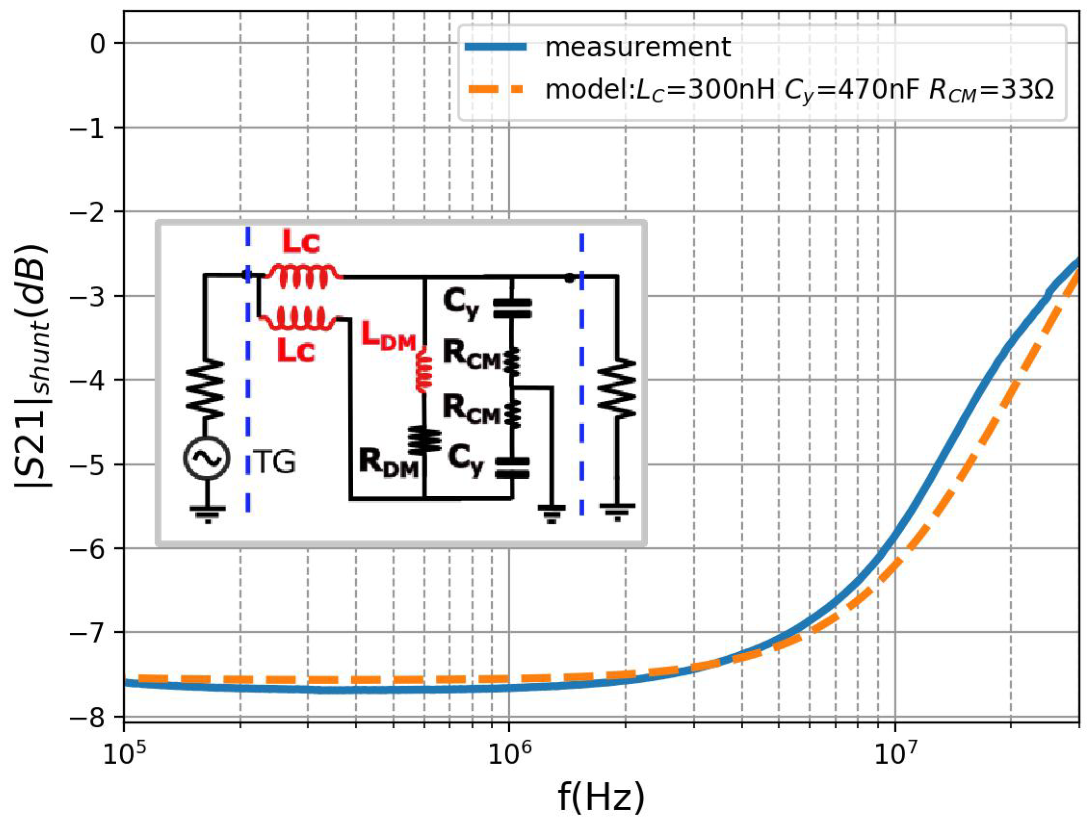
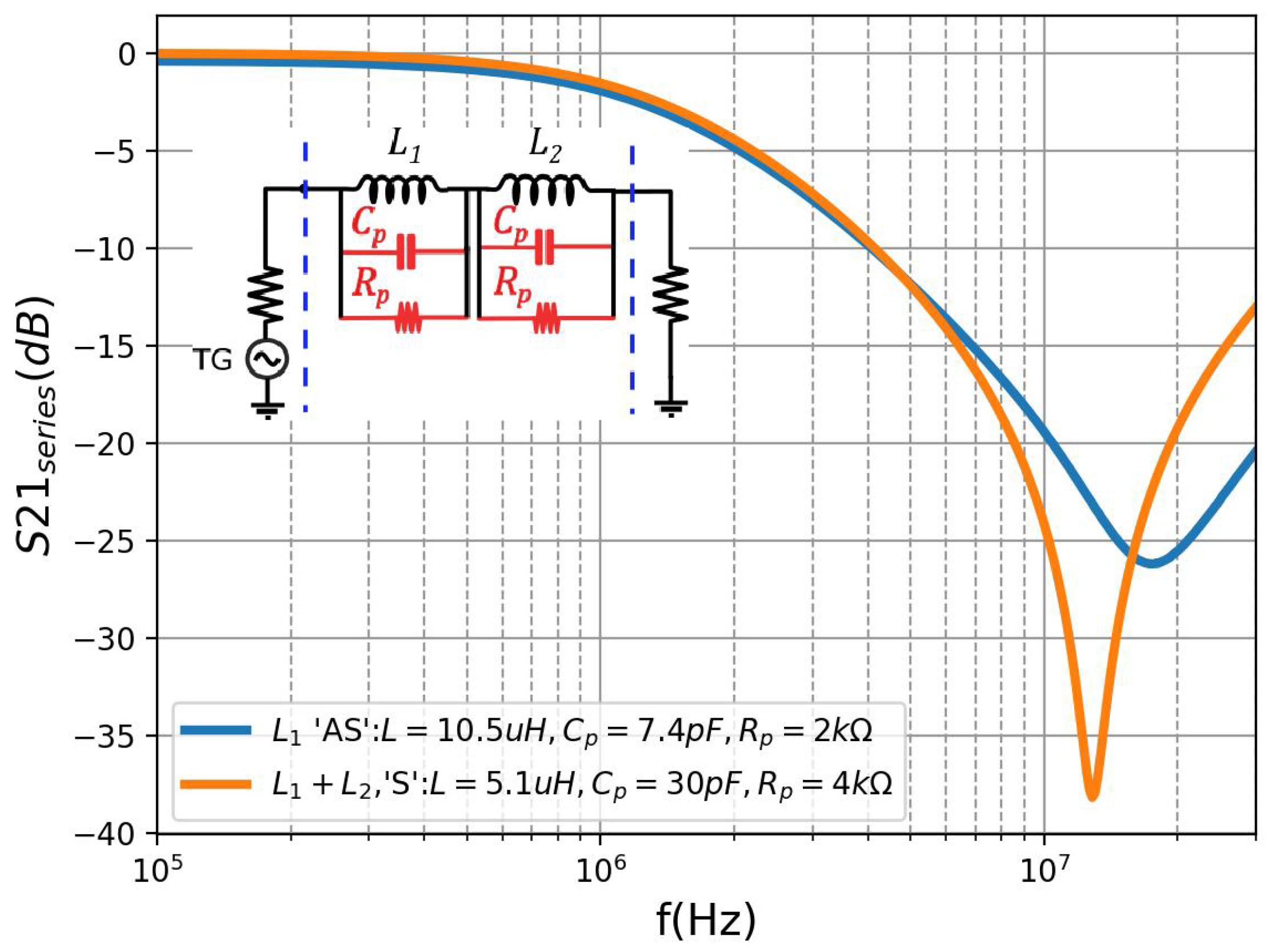
Appendix A. Extraction of Parameters of the Circuit Model

This section describes the characterization of the components of the LC filter and of the load impedance of the converter, which has been performed in the whole frequency range of interest. We have used a network analyzer to extract circuit model parameters, and also datasheet information and estimations from analytical expressions [31,32]. Circuit parameters obtained are listed in Table 3.
In Section 2.3, load impedance to ground ( Z C M , L O A D in Figure 3) was assumed to be much higher than the impedances of the connections to the chassis. In order to validate this assumption, we have measured the passive values that determine Z C M , L O A D . Figure A1 shows the transmission coefficient measured for the shunted load (with cables), along with the transmission coefficient given by the circuit model in the inset of that figure with the circuit model parameters L c , R C M shown in Table 3. Results reveal that the 33 Ω resistors in series with the load C Y capacitors are the component that determine impedance to ground from frequencies below 100 kHz and up to 5 MHz. Note that the impedance of the capacitors C Y = 470 nF is much lower than that of the 33 Ω resistors in the studied frequency range. The inductance of the output power leads becomes the dominant effect above 5 MHz. In fact, a good concordance between the measured and simulated curve is observed in Figure A1 by modeling each cable as an inductance L c 300 nH.
We have also checked the assumption than load DM impedance ( Z D M , L O A D in Figure 4) is in general much higher that filter DM impedance. In fact the extracted load inductance L D M 2 uH determines Z D M up to 6 MHz, and then up to 30 MHz, Z D M 2 R C M = 66 Ω .
Figure A1. Measured and simulated transmission coefficient S 21 of the shunted CM load with the cables.
Electronics 10 01373 g0a1
The impedance capacitor array C 0 in Figure 2 is dominated by the four 22 uF ceramic capacitors which, according to the datasheet, exhibit parasitic inductances of 3 nH. Since traces connecting these capacitors in the array are 2 cm wide, the inductance of the traces between capacitors is expected to be very low (≃1 nH). These parameters reveal that, in accordance with assumptions made in the analysis presented in Section 2, the impedance of C 0 is much lower than other filter impedances (i.e., C y ) in the whole frequency range of interest.
We have also characterized the inductors of the LC output filter. For the symmetric (‘S’) case we have used two inductors, L 1 = L 2 with an inductance of 4.7 uH (part id:‘SRP1770TA-4R7M’), and for the asymmetric (‘AS’) configuration we have used a single inductor L 1 with an inductance of 10 uH (part id: ’SER2918H-103KL’). Figure A2 shows the transmission coefficients of these inductors as measured by using the setup shown in the inset in that figure [32].
Figure A2. Transmission coefficient ( S 21 ) of the inductors L 1 and L 2 employed in ‘S’ and ‘AS’ configurations of the output LC filter of the converter.
Electronics 10 01373 g0a2
It can be observed in Figure A2 that up to 8 MHz, the series impedance of L 1 + L 2 in ‘S’ case is almost the same as that of L 1 in ‘AS’ case. Therefore, the output filters should exhibit equal responses under a purely differential excitation (i.e., V C M = 0 in Figure 2). At higher frequencies, above ≃15 MHz, the impedance of the inductors is determined by their parasitic capacitances C p . For L 1 in ‘AS’ we have obtained C p = 7.4 pF. For the ‘S’ case, the measured capacitance of both L 1 and L 2 is C p = 30 pF. As a consequence, the equivalent capacitance in a DM setup as in Figure A2 is C p / 2 = 30 / 2 pF = 15 pF, i.e., higher than for the ‘AS’ case. Therefore, under a DM excitation caused by converter operation, the symmetric (‘S’) filter is expected to provide less attenuation than the asymmetric (‘AS’) filter at frequencies above 15 MHz. This eliminates a difference on the LC output filter as a possible cause of the fact that ‘S’ outperforms ‘AS’ at reducing DM conducted emissions. Therefore, this fact can only be accounted for by the effect of the symmetric or asymmetric configuration of the LC filter on CM/DM conversion.
Other important parasitic elements in the circuit model of the converter in Figure 2 are the inductances of the cables connecting the PCB of the converter to the output connector. Those inductances are approximately L p 1 = L p 2 10 nH. Finally, as for C y capacitors, we have used thin film capacitors with values of 10 nF and 50 nF. The parasitic ESL of those capacitors given in Table 3 have been measured by following the approach described in [32].

References

  1. Krismer, F. Modeling and Optimization of Bidirectional Dual Active Bridge DC DC Converter Topologies. Ph.D. Thesis, ETH Zurich, Zurich, Switzerland, 2010. [Google Scholar] [CrossRef]
  2. Hartmann, M. Ultra-Compact and Ultra-Efficient Three-Phase PWM Rectifier Systems for More Electric Aircraft. Ph.D. Thesis, ETH Zurich, Zurich, Switzerland, 2011. [Google Scholar]
  3. Brandelero, J.C. Conception et Réalisation d’un Convertisseur Multicellulaire DC/DC Isolé Pour Application Aéronautique. Ph.D. Thesis, INP de Toulouse, Toulouse, France, 2015. [Google Scholar]
  4. Badstübner, U. Ultra-High Performance Telecom DC-DC Converter. Ph.D. Thesis, ETH Zurich, Zurich, Switzerland, 2012. [Google Scholar]
  5. Yin, S.; Tseng, K.J.; Simanjorang, R.; Liu, Y.; Pou, J. A 50-kW High-Frequency and High-Efficiency SiC Voltage Source Inverter for More Electric Aircraft. IEEE Trans. Ind. Electron. 2017, 64, 9124–9134. [Google Scholar] [CrossRef]
  6. Paul, C.R. Introduction to Electromagnetic Compatibility; Wiley: Hoboken, NJ, USA, 1992; p. 280. [Google Scholar] [CrossRef]
  7. Gammeter, C.; Krismer, F.; Kolar, J.W. Weight and efficiency analysis of switched circuit topologies for modular power electronics in MEA. In Proceedings of the 42nd Annual Conference of the IEEE Industrial Electronics Society, Florence, Italy, 23–26 October 2016; pp. 3640–3647. [Google Scholar] [CrossRef]
  8. Mihalič, F.; Kos, D. Reduced conductive EMI in switched-mode dc-dc power converters without EMI filters: PWM versus randomized PWM. IEEE Trans. Power Electron. 2006, 21, 1783–1794. [Google Scholar] [CrossRef]
  9. Mainali, K.; Oruganti, R. Conducted EMI Mitigation Techniques for Switch-Mode Power Converters: A Survey. IEEE Trans. Power Electron. 2010, 25, 2344–2356. [Google Scholar] [CrossRef]
  10. Wang, Y.; De Haan, S.W.; Ferreira, J.A. Design of low-profile nanocrystalline transformer in high-current phase-shifted DC-DC converter. In Proceedings of the IEEE Energy Conversion Congress and Exposition (ECCE 2010), Atlanta, GA, USA, 12–16 September 2010; pp. 2177–2181. [Google Scholar] [CrossRef]
  11. Wang, S.; Kong, P.; Lee, F.C. Common Mode Noise Reduction for Boost Converters Using General Balance Technique. IEEE Trans. Power Electron. 2007, 22, 1410–1416. [Google Scholar] [CrossRef]
  12. Yazdani, M.R.; Filabadi, N.A.; Faiz, J. Conducted electromagnetic interference evaluation of forward converter with symmetric topology and passive filter. IET Power Electron. 2014, 7, 1113–1120. [Google Scholar] [CrossRef]
  13. Fu, D.; Wang, S.; Kong, P.; Lee, F.C.; Huang, D. Novel techniques to suppress the common-mode EMI noise caused by transformer parasitic capacitances in dc-dc converters. IEEE Trans. Ind. Electron. 2013, 60, 4968–4977. [Google Scholar] [CrossRef]
  14. Pahlevaninezhad, M.; Hamza, D.; Jain, P.K. An improved layout strategy for common-mode EMI suppression applicable to high-frequency planar transformers in high-power dc/dc converters used for electric vehicles. IEEE Trans. Power Electron. 2014, 29, 1211–1228. [Google Scholar] [CrossRef]
  15. Chu, Y.; Wang, S. A Generalized Common-Mode Current Cancelation Approach for Power Converters. IEEE Trans. Ind. Electron. 2015, 62, 4130–4140. [Google Scholar] [CrossRef]
  16. Xie, L.; Ruan, X.; Ye, Z. Reducing Common Mode Noise in Phase-Shifted Full-Bridge Converter. IEEE Trans. Ind. Electron. 2018, 65, 7866–7877. [Google Scholar] [CrossRef]
  17. EN55025:2017/CISPR 25. Vehicles, Boats and Internal Combustion Engines—Radio Disturbance Characteristics—Limits and Methods of Measurement for the Protection of On-Board Receivers; International Electrotechnical Commission: Geneva, Switzerland, 2017. [Google Scholar]
  18. RTCA/DO-160G. Environmental Conditions and Test Procedures for Airborne Equipment; Federal Aviation Administration: Washington, DC, USA, 2005.
  19. Ott, H.W. Electromagnetic Compatibility Engineering; John Wiley and Sons Ltd.: Hoboken, NJ, USA, 1976. [Google Scholar]
  20. Gonzalez, P.; Bejarano, C.; Ramiro, S.; Bernaly, J.; Prats, M.M. Impact of output filter layout in the conducted emissions of an on-board DC/DC converter for “More Electrical Aircraft”. In Proceedings of the 11th IEEE International Conference on Compatibility, Power Electronics and Power Engineering (CPE-POWERENG), Cadiz, Spain, 4–6 April 2017; pp. 483–488. [Google Scholar] [CrossRef]
  21. Sabate, J.A.; Vlatkovic, V.; Ridley, R.B.; Lee, F.C.; Cho, B.H. Design considerations for high-voltage high-power full-bridge zero-voltage-switched PWM converter. In Proceedings of the Fifth Annual Applied Power Electronics Conference and Exposition, Los Angeles, CA, USA, 11–16 March 1990; pp. 275–284. [Google Scholar] [CrossRef]
  22. Brunoro, M.; Vieira, J.L.F. A high-performance ZVS full-bridge DC-DC 0-50-V/0-10-A power supply with phase-shift control. IEEE Trans. Power Electron. 1999, 14, 495–505. [Google Scholar] [CrossRef]
  23. Joo, D.M.; Byun, J.E.; Lee, B.K.; Kim, J.S. Adaptive delay control for synchronous rectification phase-shifted full bridge converter with GaN HEMT. Electron. Lett. 2017, 53, 1541–1542. [Google Scholar] [CrossRef]
  24. Department of Defense. MIL-STD-461G. In Requirements for the Control of Electromagnetic Interference Characteristics of Subsystems and Equipment; CreateSpace: Scotts Valley, CA, USA, 2015. [Google Scholar]
  25. Tarateeraseth, V. EMI Filter Design Part I: Conducted EMI Generation Mechanism. IEEE Electromagn. Conf. Mag. 2011, 44–50. [Google Scholar] [CrossRef]
  26. Xie, L.; Ruan, X.; Ji, Q.; Ye, Z. Shielding-Cancelation Technique for Suppressing Common-Mode EMI in Isolated Power Converters. IEEE Trans. Ind. Electron. 2015, 62, 2814–2822. [Google Scholar] [CrossRef]
  27. Bishnoi, H.; Baisden, A.C.; Mattavelli, P.; Boroyevich, D. Analysis of EMI Terminal Modeling of Switched Power Converters. IEEE Trans. Power Electron. 2012, 27, 3924–3933. [Google Scholar] [CrossRef]
  28. Gonzalez, D.; Gago, J.; Balcells, J. New Simplified Method for the Simulation of Conducted EMI Generated by Switched Power Converters. IEEE Trans. Ind. Electron. 2003, 50, 1078–1084. [Google Scholar] [CrossRef]
  29. Ferrer, L.; Balcells, J.; Gonzalez, D.; Gago, J.; Lamich, M. Modelling of Differential Mode Conducted EMI Generated by Switched Power Inverters. In Proceedings of the IECON’03, 29th Annual Conference of the IEEE Industrial Electronics Society, Roanoke, VA, USA, 2–6 November 2003; Volume 3, pp. 2312–2315. [Google Scholar] [CrossRef]
  30. Magambo, J.S.N.T.; Bakri, R.; Margueron, X.; Le Moigne, P.; Mahe, A.; Guguen, S.; Bensalah, T. Planar Magnetic Components in More Electric Aircraft: Review of Technology and Key Parameters for DC-DC Power Electronic Converter. IEEE Trans. Transp. Electrif. 2017, 3, 831–842. [Google Scholar] [CrossRef]
  31. Gonzalez-Vizuete, P.; Fico, F.; Fernandez-Prieto, A.; Freire, M.J.; Mendez, J.B. Calculation of Parasitic Self- and Mutual-Inductances of Thin-Film Capacitors for Power Line Filters. IEEE Trans. Power Electron. 2019, 34, 236–246. [Google Scholar] [CrossRef]
  32. Mendez, J.B.; Freire, M.J.; Prats, M.A.M. Overcoming the Effect of Test Fixtures on the Measurement of Parasitics of Capacitors and Inductors. IEEE Trans. Power Electron. 2020, 35, 15–19. [Google Scholar] [CrossRef]
Figure 1. PSFB topology schematic. Paths that account for CM emissions are also represented. C Y 2 accounts either for a direct bonding connection or for a capacitive coupling to the converter grounded chassis.
Electronics 10 01373 g001
Figure 2. Equivalent model of the converter at the output. In ‘S’ configurations: L 1 = L / 2 , L 2 = L / 2 . In ‘AS’ configurations: L 1 = L , L 2 = 0 . In ‘CC’ configurations: C Y 1 = C Y and C Y 2 = C Y . In ‘C0VG’ configurations: C Y 1 = C Y and C Y 2 is a short circuit. Asterisks in L 2 and C Y 2 indicate that these components might not be present depending on the filter configuration.
Electronics 10 01373 g002
Figure 3. Simplified model of the CM path, depicted from the model in Figure 2.
Electronics 10 01373 g003
Figure 4. Model to predict CM to DM conversion in the proposed filter configurations, derived from the circuit model in Figure 2.
Electronics 10 01373 g004
Figure 5. Experimental setup for measuring conducted emissions at the output leads of the converter.
Electronics 10 01373 g005
Figure 6. Measured CM output currents for symmetric (‘S’) and asymmetric (‘AS’) cases. (a) C y = 10 nF. ‘C0VG’ configuration. (b) C y = 10 nF. ‘CC’ configuration. (c) C y = 50 nF. ‘C0VG’ configuration. (d) C y = 50 nF. ‘CC’ configuration.
Electronics 10 01373 g006
Figure 7. Measured CM output currents for ‘C0VG’ and ‘CC’. (a) C y = 10 nF, ‘S’ case. (b) C y = 10 nF, ‘AS’ case. (c) C y = 50 nF, ‘S’ case. (d) C y = 50 nF, ‘AS’ case.
Electronics 10 01373 g007
Figure 8. Measured DM output currents for symmetric (‘S’) and asymmetric (‘AS’) cases. (a) C y = 10 nF. ‘C0VG’ configuration. (b) C y = 10 nF. ‘CC’ configuration. (c) C y = 50 nF. ‘C0VG’ configuration. (d) C y = 50 nF. ‘CC’ configuration.
Electronics 10 01373 g008
Figure 9. Measured DM output currents for ‘C0VG’ and ‘CC’. (a) C y = 10 nF, ‘S’ case. (b) C y = 10 nF, ‘AS’ case. (c) C y = 50 nF, ‘S’ case. (d) C y = 50 nF, ‘AS’ case.
Electronics 10 01373 g009
Table 1. Comparison for the different filter configurations studied here of the magnitudes of the expected currents flowing at the output filter, as represented in the circuit model in  Figure 4. This comparison assumes that the frequency is sufficiently low so as to make negligible the effect of parasitic inductances.
Low Frequencies
I CM I L 1 / I CM I L 2 / I CM I CO / I CM I CY 1 / I CM I CY 2 / I CM I DM , LOAD
S,CC− −0.50.5≪10.50.5− −
S,C0VG− −0.50.50.5≪11
AS,CC+ +≪110.50.50.5+
AS,C0VG+ +≪11≪1≪11
Table 2. Comparison for the different filter configurations studied here of the magnitudes of the expected currents flowing at the output filter, as represented in the circuit model in  Figure 4. This comparison assumes that frequency is sufficiently high as to make significant the effect of parasitic inductances. Signs + and − in the table account for comparatively high and low currents, respectively.
High Frequencies
I CM I L 1 / I CM I L 2 / I CM I CO / I CM I CY 1 / I CM I CY 2 / I CM I DM , LOAD
S,CC− −0.50.5≪10.50.5− −
S,C0VG− −0.50.5<0.5<0.5>0.5
AS,CC+ +≪110.50.50.5+
AS,C0VG+ +≪11<0.5<0.5>0.5+ +
Table 3. Parameters of the output filter and load setup.
L 1 , L 2 ‘S’ L 1 , ‘AS’
L (μH) C p  (pH) R p  (k Ω )L (μH) C p  (pH) R p  (k Ω )
10.57.425.1304
L SC , ‘C0VG’ C o C Y ‘10 nF’ C Y ‘50 nF’
L (nH)C (μF)C (nF)L (nH)C (nF)L (nH)
<58810105020
L p 1 , L p 2 Load
L (nH) R D M ( Ω ) L D M (μH) L c (nH)RCM ( Ω ) C Y (nF)
101230033470
Publisher’s Note: MDPI stays neutral with regard to jurisdictional claims in published maps and institutional affiliations.

