Article

Buck-Boost Charge Pump Based DC-DC Converter †

1
Department of Electrical and Computer Engineering, University of Thessaly, 383 34 Volos, Greece
2
Department of Electrical and Computer Engineering, University of the Peloponnese, 263 34 Patras, Greece
3
Electronics Laboratory, Department of Physics, University of Patras, 265 04 Patras, Greece
*
Authors to whom correspondence should be addressed.
This paper is an extended version of our paper published in the 2022 Panhellenic Conference on Electronics & Telecommunications (PACET). Keramida, E.; Souliotis, G.; Vlassis, S.; Plessas, F. Buck-Boost Charge Pump based DC-DC converter. In Proceedings of the 2022 Panhellenic Conference on Electronics & Telecommunications (PACET), Tripolis, Greece, 2–3 December 2022; pp. 1–5. https://doi.org/10.1109/PACET56979.2022.9976361.
J. Low Power Electron. Appl. 2023, 13(2), 27; https://doi.org/10.3390/jlpea13020027
Submission received: 28 February 2023 / Revised: 12 April 2023 / Accepted: 19 April 2023 / Published: 21 April 2023

Abstract

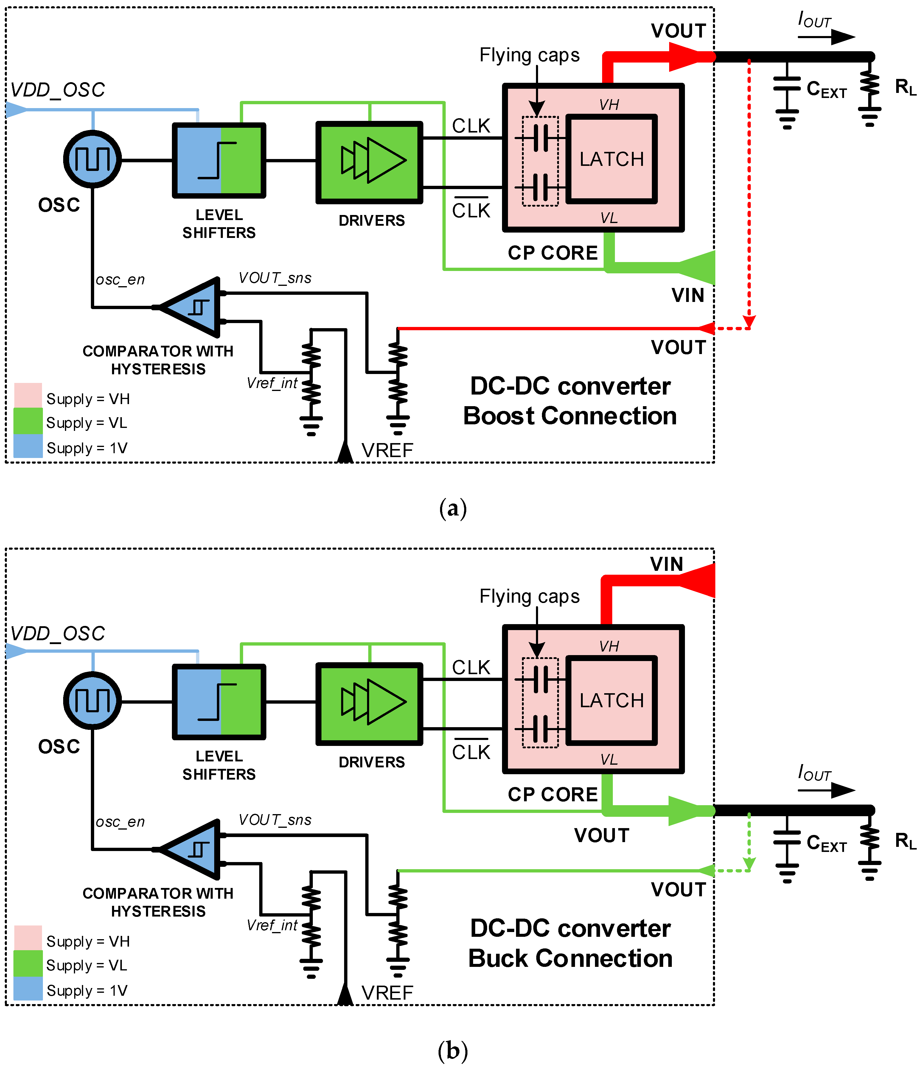
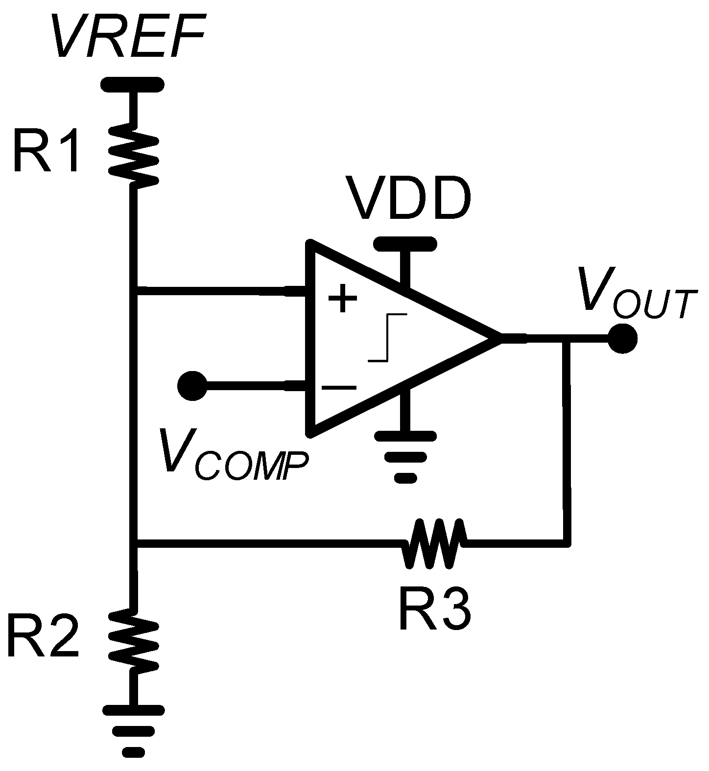
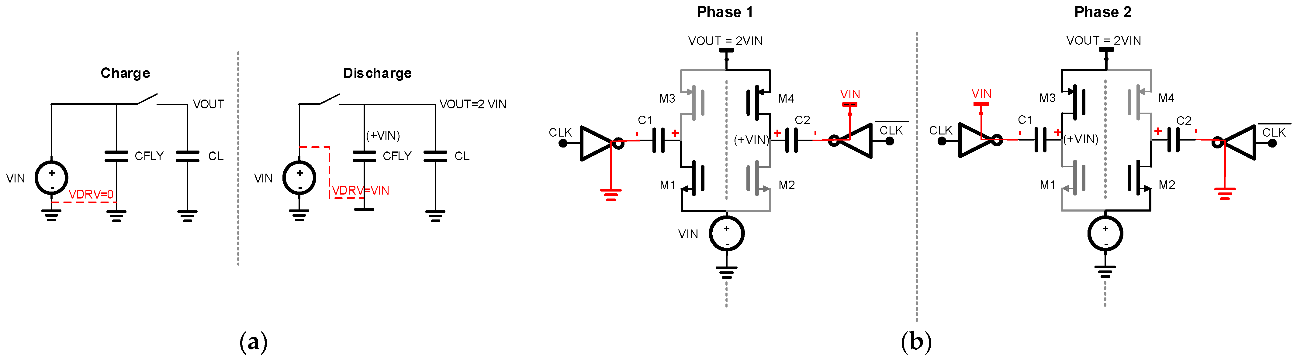
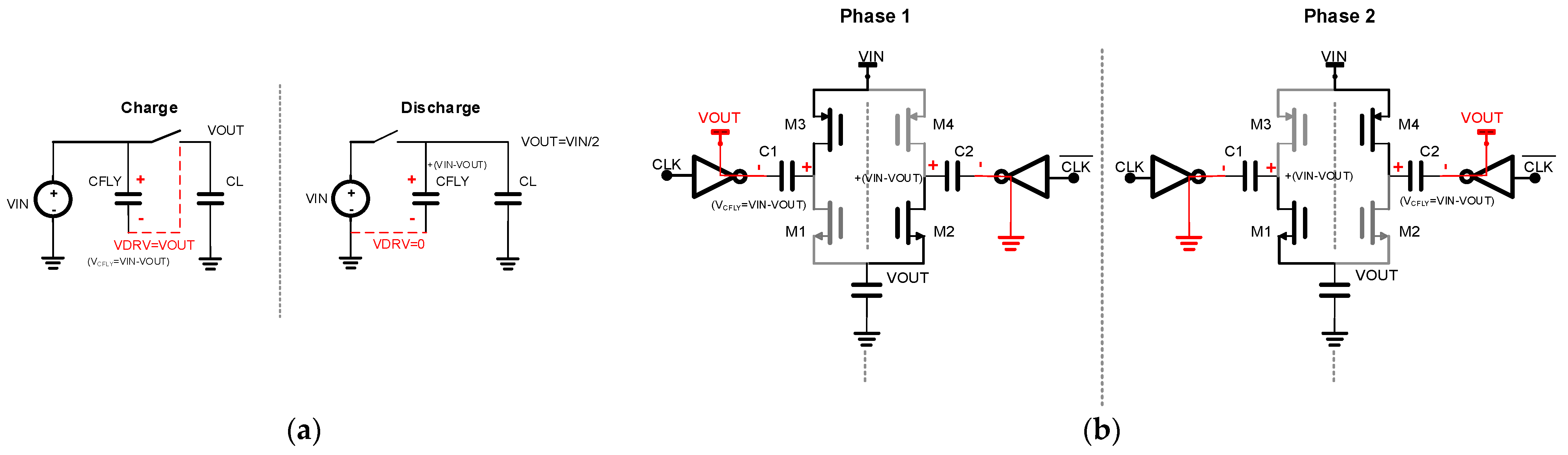
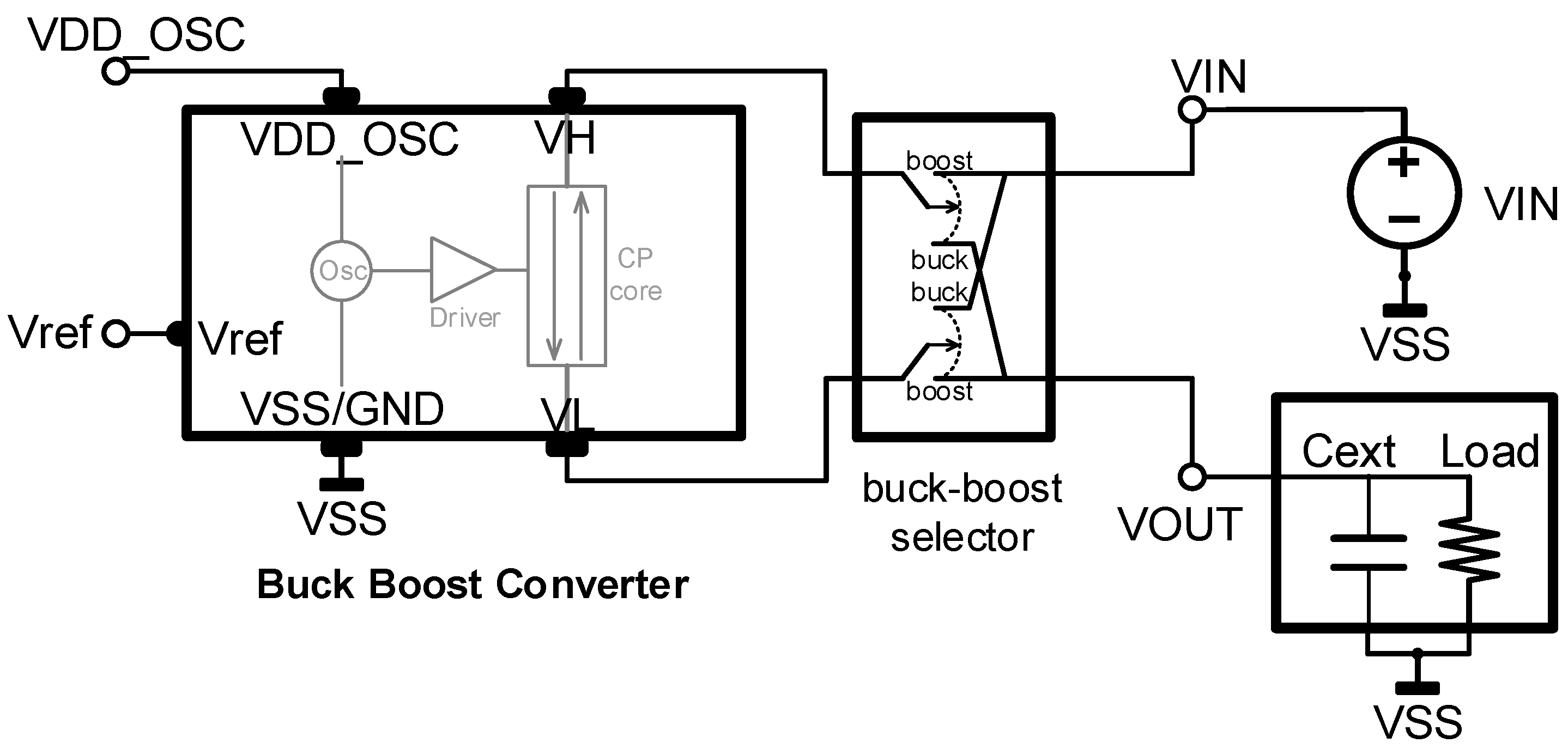
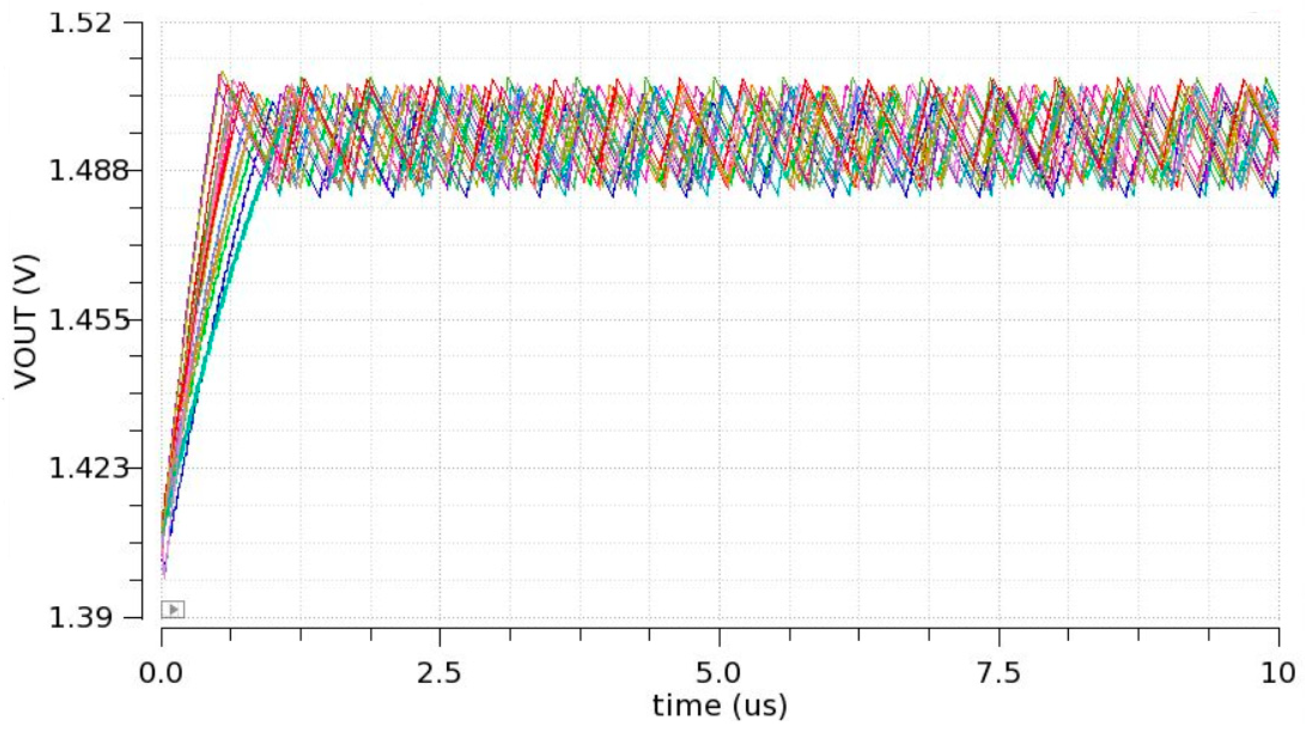
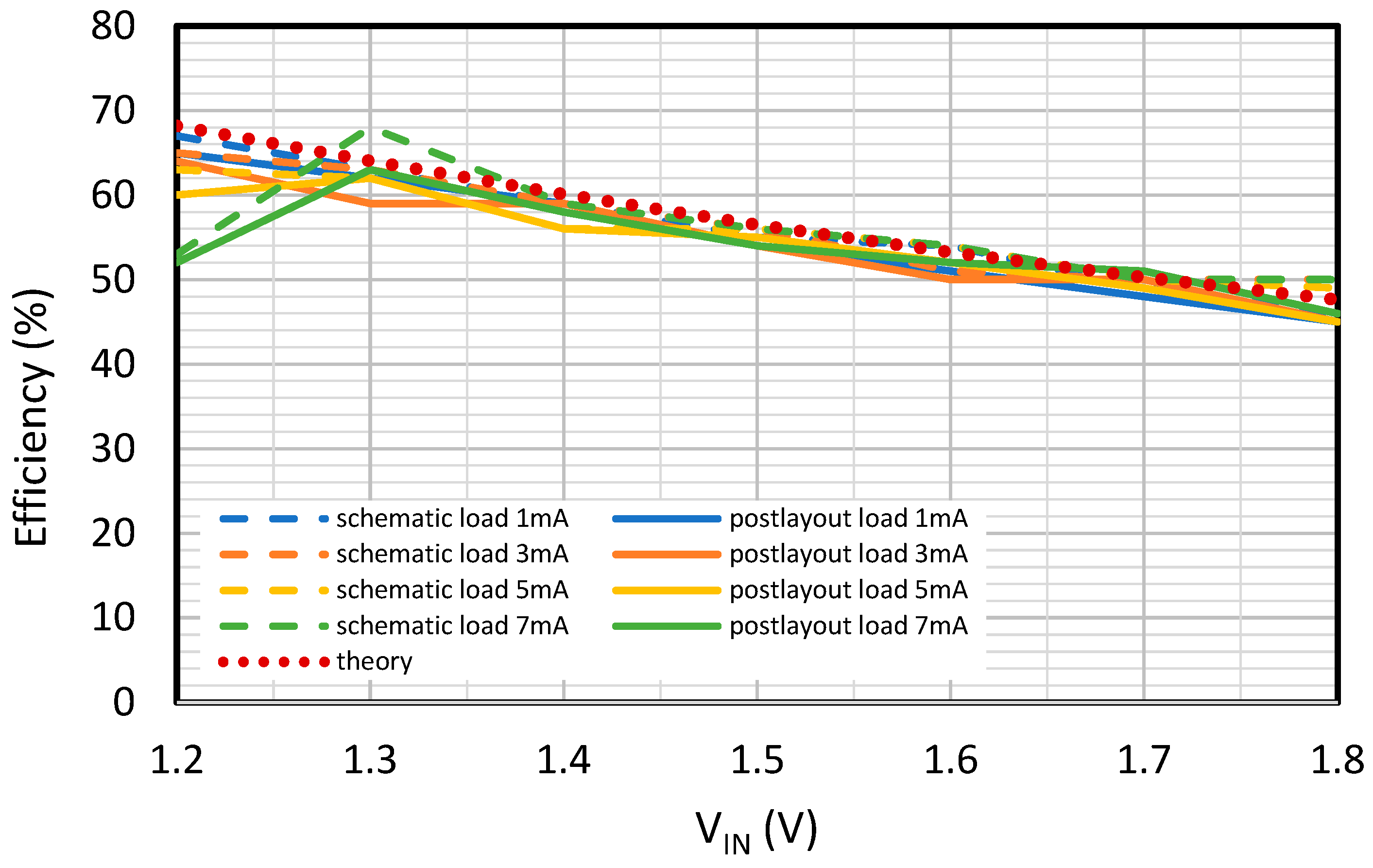
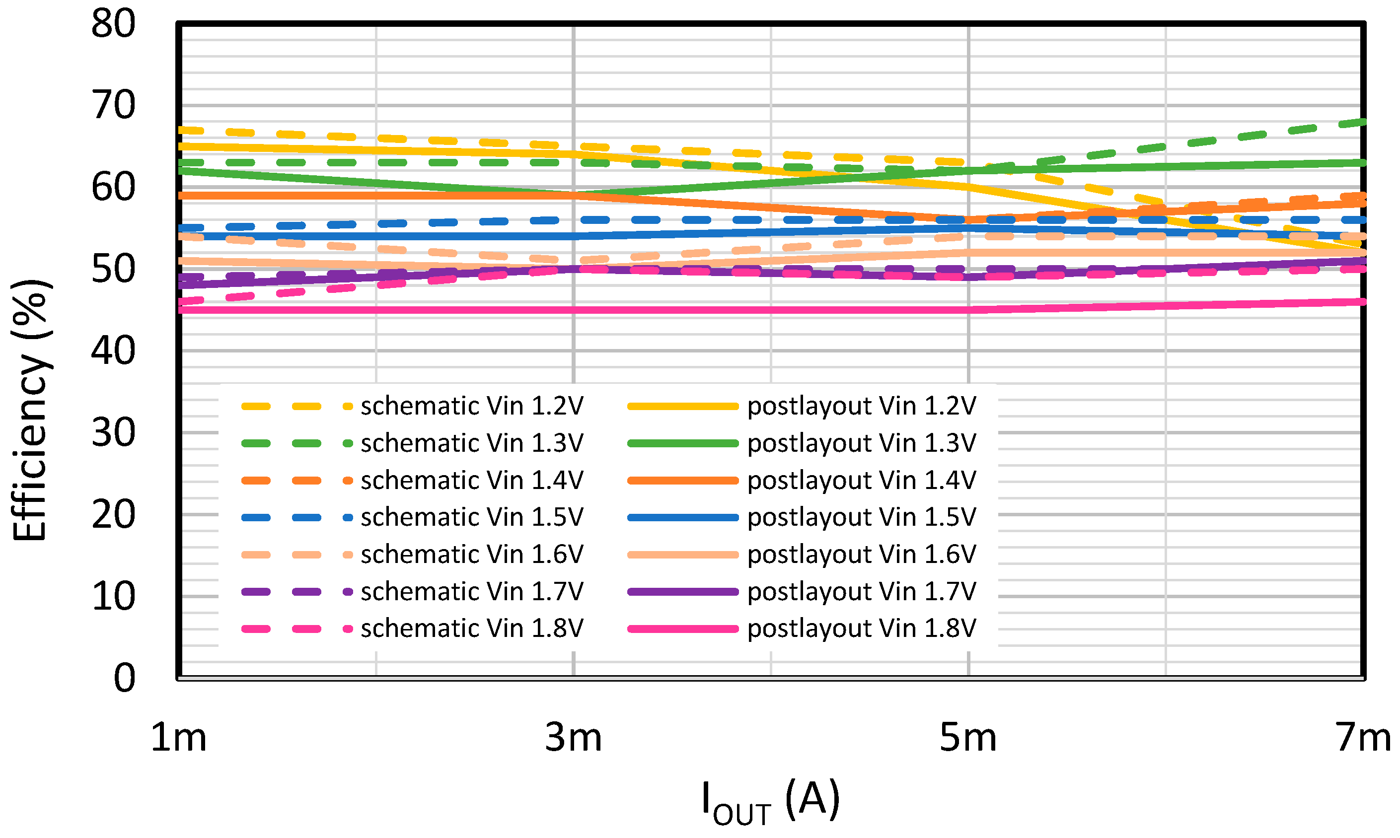
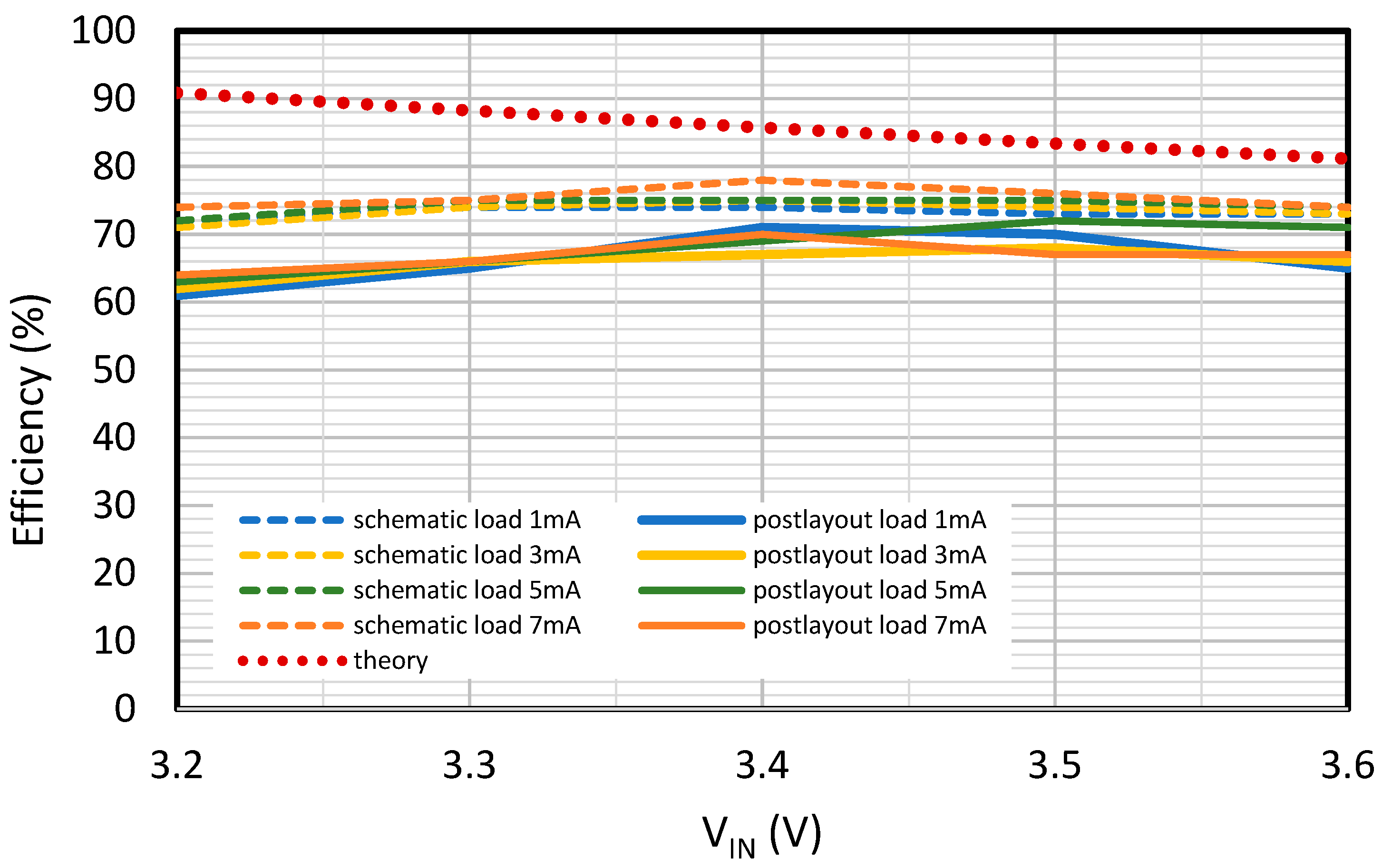
This paper presents a novel inductorless dual-mode buck-boost charge pump (CP) based DC-DC converter. The proposed architecture allows the same circuit to accomplish two modes of operation, buck and boost, for degrading or elevating the output voltage, respectively, compared to the input. To achieve each mode, only a switching of the input–output connections is needed without any other modification in the design of the DC-DC converter. The dual-mode configuration aims to merge two different functions into one circuit, minimizing the design time and the area the DC-DC converter occupies on the die. The proposed buck-boost CP has been designed using TSMC 65 nm complementary metal–oxide–semiconductor (CMOS) technology. The functional input voltage range of the CP in boost mode is 1.2 V to 1.8 V and the typical output voltage is 1.8 V. For the buck mode, the input voltage range is 3.2 V to 3.6 V and the output is 1.5 V. For both modes, the output can be easily modified to new values by changing the comparator configuration. Efficiency results are also provided for the two modes.
Keywords: switched capacitor converter; dual-mode charge pump; buck-boost DC-DC converter; power management switched capacitor converter; dual-mode charge pump; buck-boost DC-DC converter; power management