Article

A Time-Mode PWM 1st Order Low-Pass Filter †

by
Konstantinos P. Pagkalos
*,
Orfeas Panetas-Felouris
and
Spyridon Vlassis
Electronics Laboratory, Physics Department, University of Patras, 26504 Patras, Greece
*
Author to whom correspondence should be addressed.
This paper is an extended version of our paper publish in Pagkalos, K.P.; Panetas-Felouris, O.; Vlassis, S. Charge-Based Time Registers for z−1 Implementation. In Proceedings of the 2022 6th Panhellenic Conference on Electronics and Telecommunications (PACET), Tripolis, Greece.
J. Low Power Electron. Appl. 2023, 13(2), 32; https://doi.org/10.3390/jlpea13020032
Submission received: 20 March 2023 / Revised: 26 April 2023 / Accepted: 3 May 2023 / Published: 6 May 2023

Abstract

:
In this work, a first-order low-pass filter is proposed as suitable for time-mode PWM signal processing. In time-mode PWM signal processing, the pulse width of a rectangular pulse is the processing variable. The filter is constructed using basic time-mode building blocks such as time registers and time adders and so it is characterized by low complexity which can lead to the modular and versatile design of higher-order filters. All the building blocks of the filter were designed and verified in a TSMC 65 nm technology process. The sampling frequency was 5 MHz, the gain of the filter at low frequencies was at −0.016 dB, the cut-off frequency was 1.2323 MHz, and the power consumption was around 59.1 μW.

1. Introduction

Analog circuits are continuously losing benefits through technology scaling. The reduction of the voltage headroom has resulted in limitations in the voltage swing of analog signals. In addition, the shrinkage of the channel length of transistors makes analog circuits vulnerable to non-linearities and current leakage. On the other hand, digital circuits are benefiting from the constant device scaling, improving their processing speed and resolution due to the superiority of time resolution to the voltage equivalent in these processes [1,2].
An interesting alternative to conventional analog circuits is time-mode circuits. The difference in this procedure is that the information is expressed in the field of time instead of voltage or current as it happens in the typical approaches. There are two types of time-mode processing with respect to the way that the information is represented. In the first, the information is expressed as the time interval between the positive edges of two pulse signals. In the second, the information is represented by different values of the pulse widths (PWM) of a pulse [3]. The advantages of time-mode circuits are that they are constructed by standard digital logic gates, which benefit from the device scaling due to the superiority of time resolution and are not affected by voltage supply reduction.
A block diagram of a time-mode system suitable for pulse-width modulation signal processing is presented in Figure 1. Firstly, a voltage-to-time converter (VTC) is employed to convert the analog continuous-time signal Vin into a time-mode signal Tin [4,5]. The VTC consists of a sample-and-hold circuit that samples the continuous voltage signal with a sampling period Ts and a pulse-width modulator that converts every voltage sample into a rectangular pulse. The input signal of the time-mode unit will actually be a pulse train in which every pulse will have the same frequency as the sampling signal, but the pulse width will be equal to a linear function of the corresponding voltage sample. After the conversion, the information is processed in the time mode. The time-mode processing unit could include many simple operations like a z−1 operation, addition, subtraction, amplification [6], or multiplication [7,8]. Furthermore, a combination of these simple operations can be achieved if more complex processing is needed (e.g., time-mode filtering [9,10,11] and time-mode integrators [12,13,14]). Finally, the processed time-mode signal is converted back to the voltage mode via a time-to-voltage converter (TVC). It should be mentioned that the processed time-mode information can be quantized via a time-to-digital converter (TDC) if further processing is needed by a digital signal processing unit [15,16,17].
Analog signal filtering is very important in many applications such as sensor interfaces, wireless transceivers, and signal/image processing. Low-order filters can be used in systems where the cut-off frequency is relaxed, offering low complexity and a small layout area. According to the author’s best knowledge, there is no implementation of a first-order low-pass filter that operates in time mode, already published in the literature. This is the main contribution made in this work.
More specifically, this work presents a time-mode first-order low-pass filter as a design example suitable for time-mode signal processing (TMSP). The circuit consists of a time-mode z−1 operator and a z−1 weighted time-mode adder with gain ½. All the building blocks of the z−1 operator and the weighted time adder are based on the time-register circuit. The low-pass filter is achieving the desired operation over process and temperature corners. Lastly, it is characterized by modular design, so it can be used as a building block for higher-order filters.
The paper is organized as follows. In Section 2, the top-level topology of the low-pass filter is presented as well as the time-mode building blocks that the filter consists of. In Section 3, a brief presentation of the digital calibration loop is presented which was used in order to achieve the desired frequency response, phase response, and cut-off frequency over process and temperature corners. Section 4 presents the simulation results to evaluate the filters’ behavior with respect to their frequency response, phase response, cut-off frequency, and power consumption. Finally, the conclusions from this work are presented in Section 5.

2. Implementation of the Time-Mode PWM Low-Pass Filter

2.1. Top-Level Architecture

The proposed top-level topology of the time-mode PWM low-pass filter is presented in Figure 2a. The circuit architecture, which is presented in Figure 2b, consists of a z−1 operator and a z−1 time adder with a gain equal to ½. The operation principle is based on the application of z-transformation to the analog circuits and systems [18]. The timing diagram of the circuit is presented in Figure 2c. The first input of the time adder receives the input signal directly and so the Tint.1(k) signal will be equal to the Tin(k) signal. It is assumed that the input signal is basically a pulse train in which every pulse has the same frequency as the sampling signal and is synchronous with it. On the second input of the time adder, the input pulse train is first passed through a z−1 operator which delays every input pulse by one sampling clock and then it is connected on the second input of the time adder. Hence, the node Tint.2(k) will be equal to:
T i n t .2 ( k ) = T i n ( k 1 )
Lastly, the time adder sums the two inputs and multiplies their product with a weight equal to ½. The time adder also adds one more time delay, which is equal to the sampling clock, to both input signals due to its inherent z−1 operation. As a result, the relationship between the output pulse width Tout and the input pulse width Tin of the low-pass filter is:
T o u t ( k ) = 1 2 [ T i n t .1 ( k 1 ) + T i n t .2 ( k 1 ) ] = 1 2 [ T i n ( k 1 ) + T i n ( k 2 ) ]
where k is the time index. The z-domain transfer function of the above input–output equation is:
H ( z ) = z 1 2 ( z 1 + 1 )
At low frequencies, the signal time delay, which is always equal to one sampling clock due to the z−1 operation, is small compared to the period of the input signal. Hence, for those frequencies, the z−1 variable of Equation (3) is approximately equal to unity and therefore the gain of the impulse response that is described by Equation (3) will be approximately equal to 1. As the frequency increases, the time delay of the input signal becomes comparable to the sampling period. At the point where the frequency of the input signal becomes half the sampling frequency, the input signals of the time adder will have a 180° difference in phase. Therefore, their sum will be neglected and the gain of the transfer function will be zero. Therefore, the z-domain transfer function that was mentioned in Equation (3) describes a low-pass filter behavior in which, for frequencies sufficiently lower than the sampling frequency, the input signal will pass to the output and, for frequencies compared to the sampling frequency, the input signal will be attenuated [18]. It should be mentioned that for frequencies above half of the sampling frequency, the transfer function rebounds due to the aliasing effect as happens in many discrete-time systems. Thus, an anti-aliasing filter is needed during the reconstruction of the information to the voltage mode [18].
Finally, the transfer function of an ideal discrete time z-domain low-pass filter is given by H(z) = (½)(z−1 + 1) because it is assumed that the time adder does not add a time delay. Comparing the aforementioned equation with Equation (3), an extra phase difference between the output and input signals will be expected due to the additional delay added by the time adder.

2.2. Time-Mode PWM Building Blocks

2.2.1. Time Register Based on Gate-Controlled Current Source

The time register that has been used is based on the gate-controlled approach that is presented in Figure 3 [19]. The behavior of the time register is based on the constant discharging slope of capacitor C. The Tset signal is equal to the sampling signal. During the time where Tset = ‘0’ (‘0’ means asserted to the ground), the capacitor is connected to the supply via transistor M1 which acts as a switch. Hence, the capacitor is charged to the voltage supply VDD. On the other hand, when Tset = ‘1’ (‘1’ means asserted to the voltage supply), there are three distinct operations of the circuit. During the time interval of which Tin = ‘1’, the capacitor is discharged via transistor M2 which acts as a current source, delivering constant discharging current equal to Iref. The current Iref that the current source delivers is controlled by its’ gate voltage VCTRL. The gate voltage of M2 is controlled through switches in order to be connected to VCTRL or to the ground with respect to digital control signal TRin, where TRin = Tin + Tclk due to the OR gate. The value of the discharging capacitors’ slope is equal to:
s l p = I r e f C
At the time when both Tin = ‘0’ and Tclk = ‘0’ (they are both equal to zero voltage), the capacitor is floating and hence voltage Vcap remains constant. Finally, during the time interval of which Tclk = ‘1’, the capacitor is also discharging with the constant slope described in Equation (4). During Tclk = ‘1’ and when the voltage on the top plate of capacitor C crosses the reference voltage Vtp of the comparator, the latter changes state. The digital logic that follows the comparator results in an output pulse with a frequency equal to Tset while the phase between those two is equal to 180°. The pulse width of the output will be:
T o u t . r e g ( k ) = T c l k T i n ( k 0.5 )

2.2.2. Time-Adder Core Implementation with Gain ½

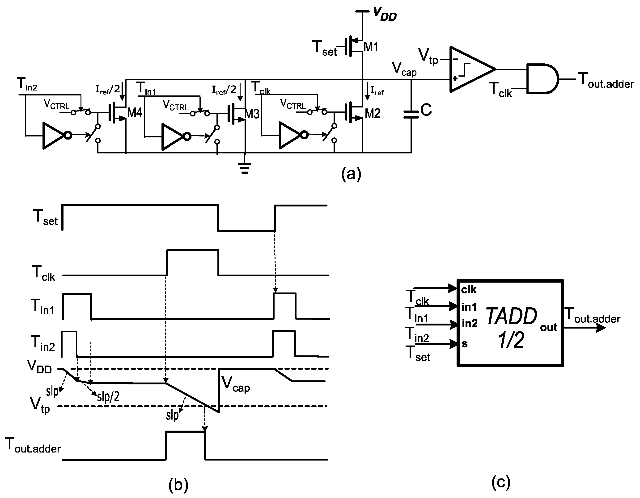
The time-adder core with gain ½ is presented in Figure 4. The operation principle of the circuit is based on the gate-controlled time register that is described earlier.
The difference here is that there are three discharging branches that deliver constant discharging currents with magnitudes equal to Iref/2, Iref /2, and Iref, respectively. For this option, there are three different operations that affect the value of the discharging slope. At the time interval where Tin1 = ‘1’ and Tin2 = ‘1’, transistors M3 and M4 are both open and deliver constant discharging current. As a result, the total discharging current of the capacitor will be equal to Iref and the value of the discharging slope will be given by Equation (4). When only one of the two inputs is connected to the supply, then the discharging current will drop to half and so will decrease the value of the discharging slope. Finally, during Tclk = ‘1’, the circuit will have the same behavior as it had on the simple time register. Hence, every input signal will result in half of the voltage drop across the capacitor compared with the voltage drop from the Tclk signal. As a result, on the output of the time adder with gain ½, a pulse will be generated which will be delayed by half of a period of the Tset signal and with an output pulse width equal to:
T o u t . a d d e r ( k ) = T c l k + 1 2 [ T i n 1 ( k 0.5 ) + T i n 2 ( k 0.5 ) ]

2.2.3. Implementation of a z−1 Operator Using a Time Register

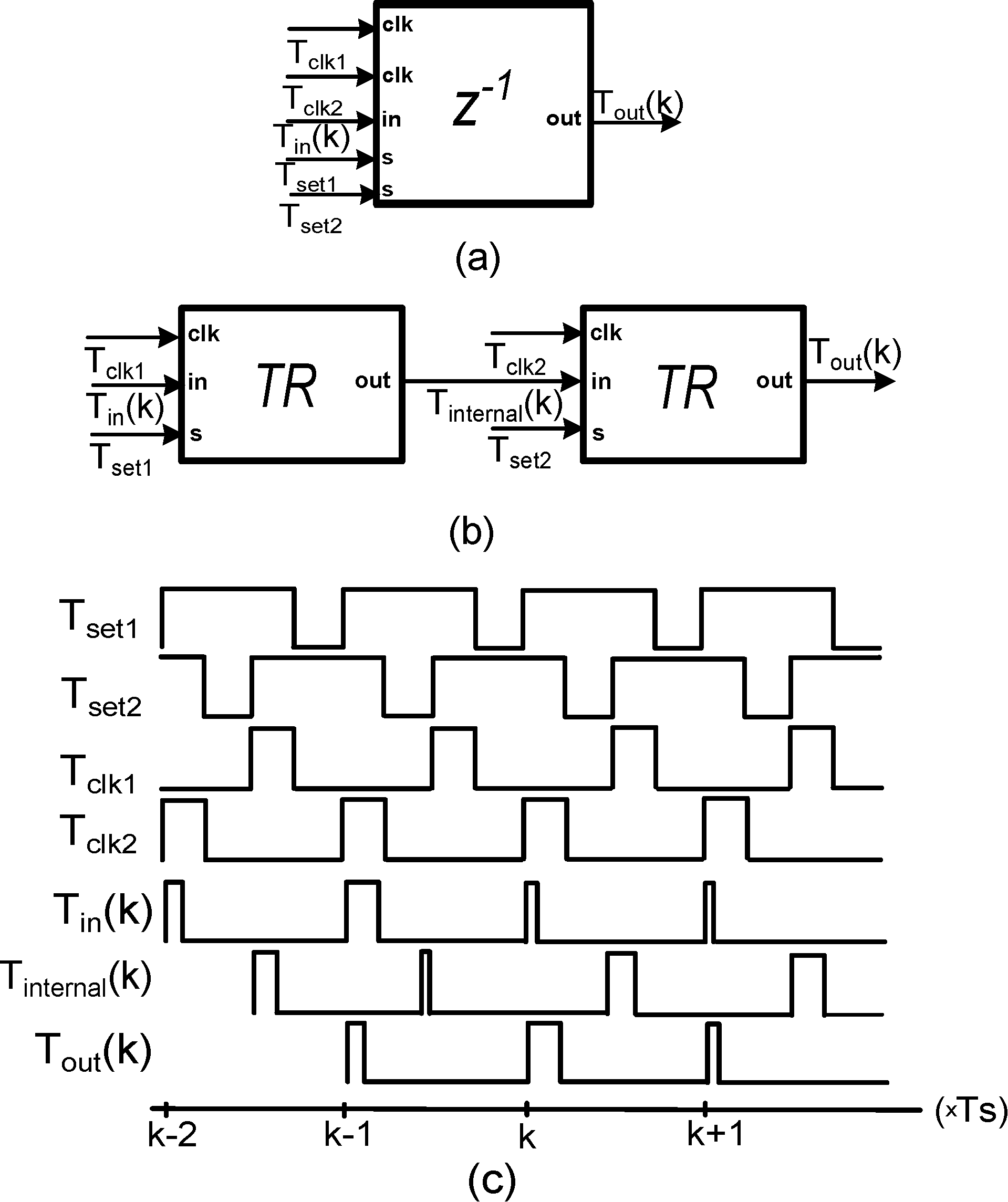
The z−1 operation is achieved by employing two cascaded time registers as presented in Figure 5. For the z−1 operation, the architecture which employs two cascaded time registers is selected instead of the architecture which uses four, in order to achieve less layout area, lower power consumption, and larger resolution [19].
The Tset1 signal (sampling signal) and the Tset2 signal have the same pulse width but with a phase difference equal to 180°. Furthermore, the Tclk1 and Tclk2 signals have the same pulse width but with phases equal to 180° and 0°, respectively, with respect to the sampling signal (Tset1 signal).
The front-end time register receives an input pulse Tin, synchronous with the sampling signal, and produces an output pulse Tinternal delayed by half of a period of the Tset1 signal and with a pulse width equal to the complementary value of Tin in respect to Tclk:
    T i n t e r n a l ( k ) = T c l k T i n ( k 0.5 )
The second time register receives Tinternal and produces output pulses delayed by half of a period of the Tset2 signal and with a pulse width equal to the complementary value of Tinternal with respect to Tclk. As a result, the output pulse of the whole z−1 operator will be a pulse delayed by one Tset1 clock and with a pulse width equal to the inputs’ pulse width:
T o u t ( k ) = T c l k T i n t e r n a l ( k 1 ) = T i n ( k 1 )

2.2.4. Implementation of the z−1 Time Adder with Gain ½

The implementation of the z−1 time adder with time gain ½ is illustrated in Figure 6. The Tset1 signal is the sampling signal. In the implementation of the time adder, the time register is replaced by the time-adder core with gain ½ that was described earlier. As a result, the internal signal of the circuit will also be a pulse delayed by half of a period of the sampling signal but with a pulse width equal to the complementary value of half of the sum of the two inputs Tin1 and Tin2 of the time-adder core with respect to the Tclk signal:
T i n t e r n a l ( k ) = T c l k + 1 2 [ T i n 1 ( k 0.5 ) + T i n 2 ( k 0.5 ) ]
The time register has the same behavior as it had on the z−1 operation, shifting the Tinternal signal by half of a period of the Tset1 signal and producing an output pulse with a pulse width equal to:
T o u t ( k ) = T c l k T i n t e r n a l ( k 0.5 ) = 1 2 [ T i n 1 ( k 1 ) + T i n 2 ( k 1 ) ]
Hence the output of the circuit will be a pulse delayed by sampling signal and with a pulse width equal to half of the sum of the two inputs of the circuit.

3. Discharging Slope Digital Calibration

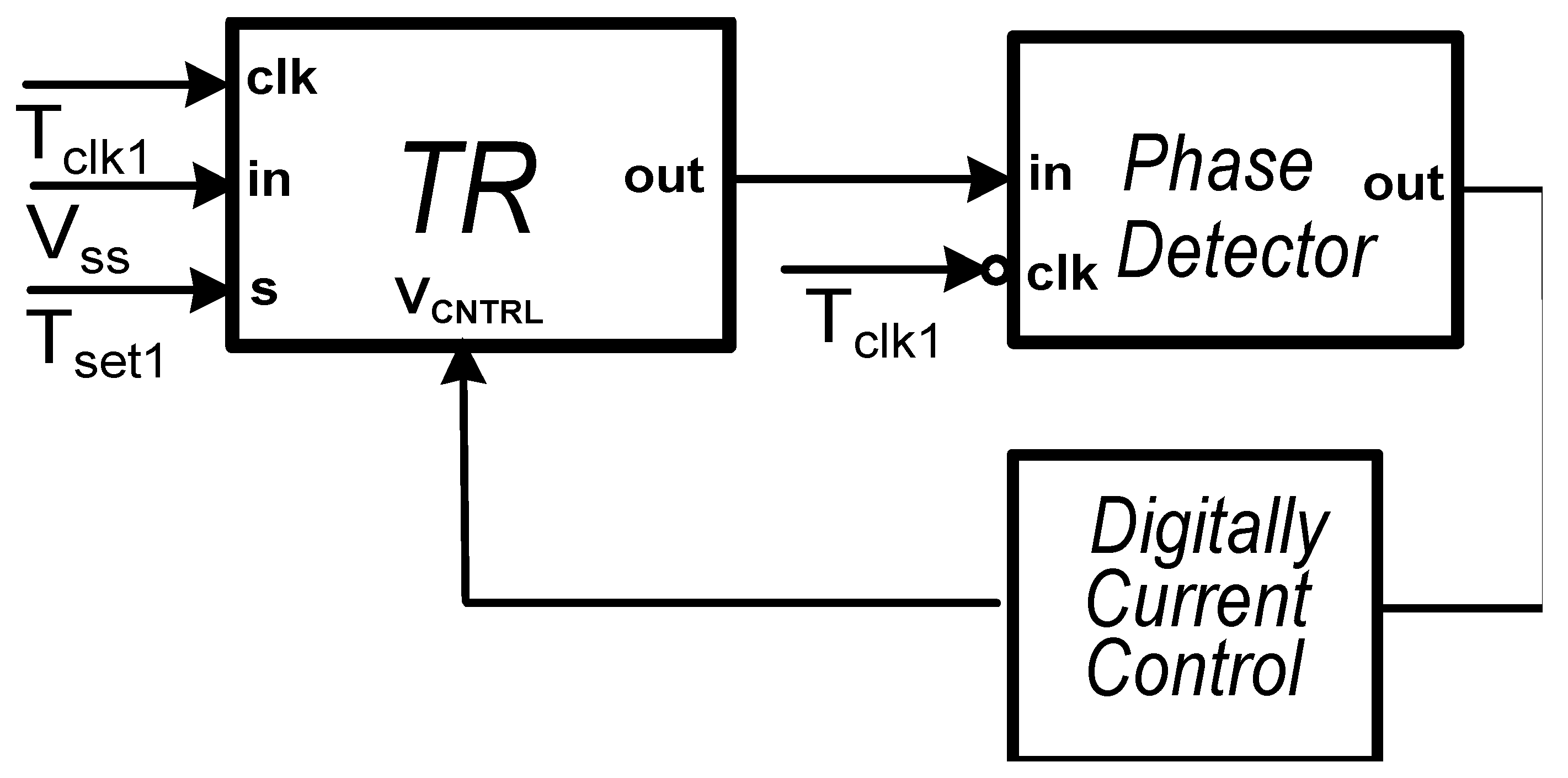
The value of the constant discharging slope of the time register and time-adder with gain ½ must be well defined for the maximum available input range to be achieved by the time-mode building blocks [19]. However, the discharging current and, also, the capacitor’s capacitance that directly affects the value of the discharging slope are sensitive to process (P) and temperature (T) variations (PT variations). To compensate for the PT variations of the discharging slope, a digitally controlled calibration loop is adopted as described in [20] and briefly presented in Figure 7.
Briefly, in this calibration loop, the discharging current is controlled by an 8-bit digital control code. At the beginning of the calibration, the digital code takes its minimum value, generating the minimum value for the discharging current of the time register. In each calibration cycle, the value of the digital code (and the discharging current) increases until, during a time interval of the Tclk signal, the capacitor voltage drops from the voltage supply to the triple point of the leading comparator. At this point, the digital code stops increasing and locks to a specific value, delivering the desirable constant discharging current to achieve maximum input range.

4. Simulation Results

The low-pass time-mode filter was designed and described with respect to its frequency response, cut-off frequency, phase response, and power consumption over PT corners. The circuit was designed using the Cadence Virtuoso environment and simulated using the Spectre simulator. The time-mode building blocks were designed using the TSMC 65 nm technology process. The voltage supply was set in 1.2 V and the sampling frequency was equal to 5 MHz. The capacitor value in every time-mode building block was 2 pF. Transistor M1 size was selected to be 650 nm/260 nm in order to deliver enough current to charge the output capacitor and to have relatively large resistance when it is in the off state. Transistors M2, M3, and M4 had lengths equal to 2 μm in order to be characterized by large gate-to-source resistance and work as current sources. They also had widths equal to 2 μm, 1 μm, and 1 μm, respectively, to deliver discharging current equal to Iref, Iref/2, and Iref/2 accordingly.
In Figure 8, the testbench that was used to simulate the behavior of the low-pass filter is presented. The VTC converts the input signal from voltage mode to time mode and the TVC converts the time-mode signal to the voltage-mode. These two blocks are ideal Verilog-A models in order to not disturb the performance metrics. On the input of the entire system, a sinusoidal signal is applied equal to Vin = 0.5   V D D + V i n . p e a k   sin(2πfin · t), where 0.5 VDD is the average voltage, Vin.peak is the amplitude, and fin is the input frequency. The VTC converts this signal into a pulse train in which every pulse has magnitude:
T i n ( t ) = 25   ns + T i n . p e a k sin ( 2 π f i n t )  
where Tin.peak is the corresponding pulse magnitude width and ranges from 0 to 25 ns. Therefore, the width of every pulse ranges from 0 to 50 ns in a sinusoidal manner.
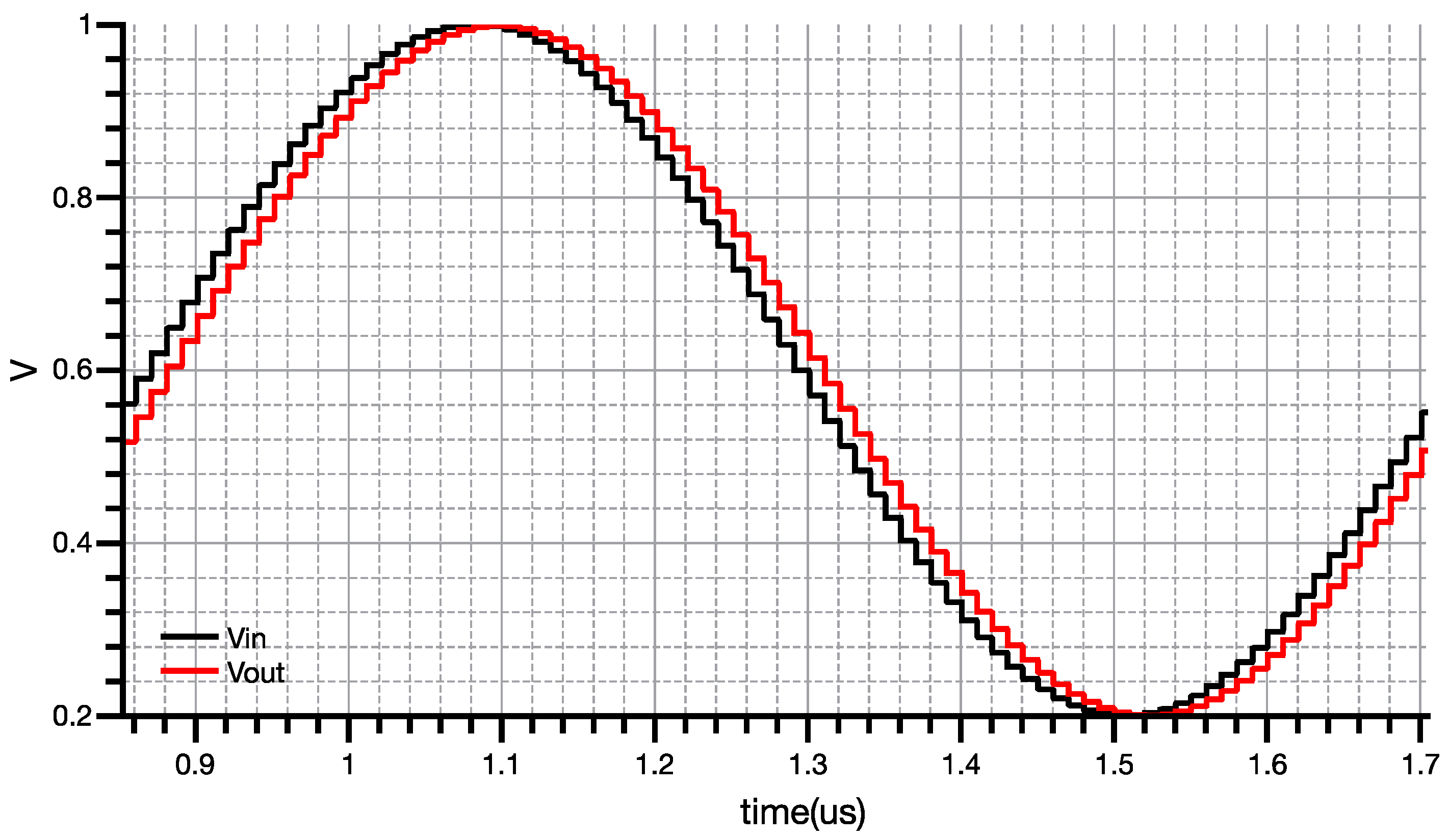
In Figure 9, the transient response of the input and the output are presented for a signal with a frequency equal to 58.59375 kHz. As can be seen, the input and the output signals have equal magnitudes, since the input signal has a frequency much smaller than the sampling frequency. Hence, the filter achieves unit gain for small frequency signals, verifying the correct behavior of the filter in this frequency range. The output signal is delayed by one sampling clock period due to the z−1 operation which is inherent to the time adder.
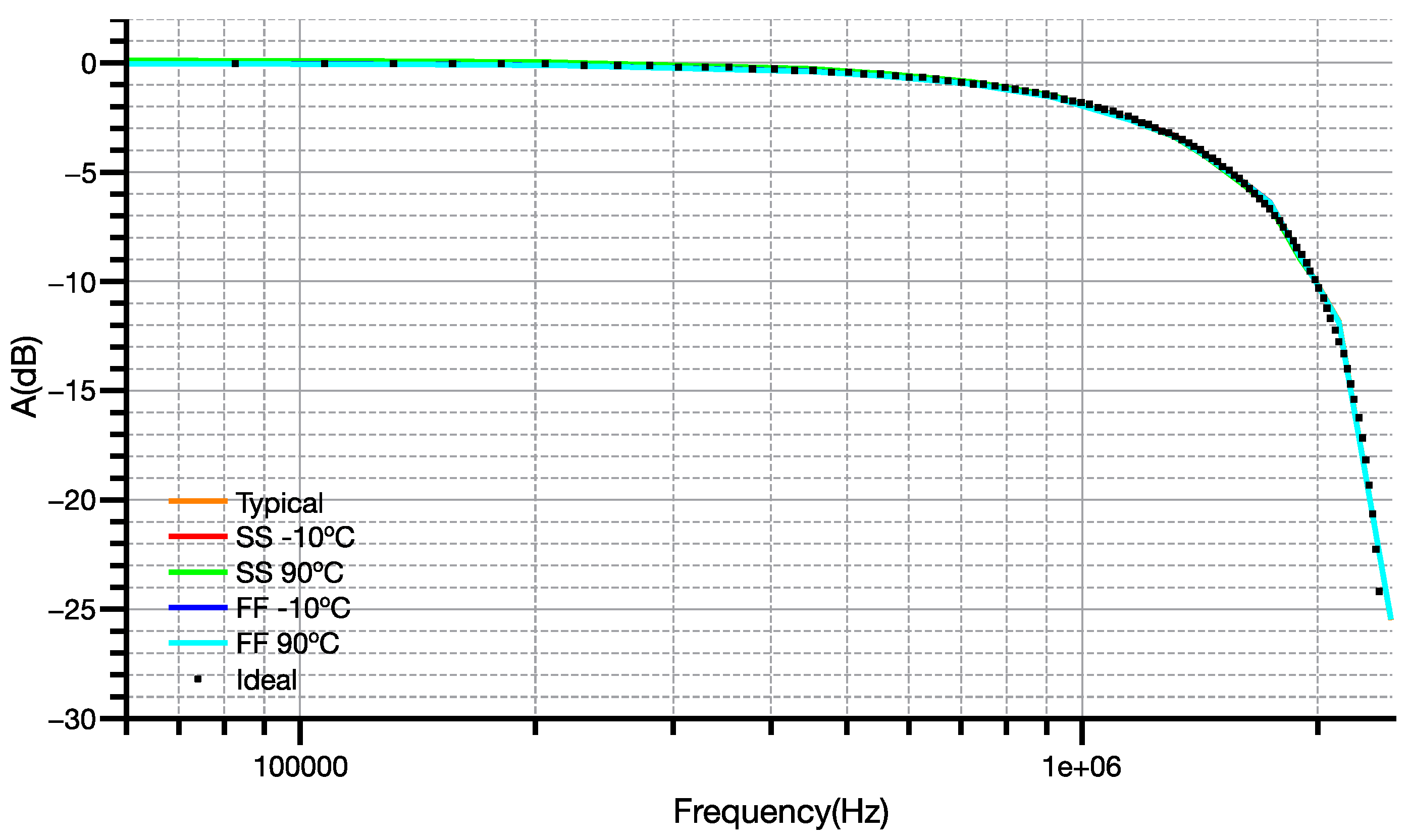
In Figure 10, the frequency response over PT corners of the first-order low-pass filter for a frequency range between 10 kHz and 2.5 MHz is presented. The filter’s gain response for several input frequencies was measured by employing discrete Fourier transform (DFT) on the input and output signals of the system that is presented in Figure 8. The formula that was used to calculate the gain response is:
A d B = A o u t . f 0 A i n . f 0  
where f0 is the fundamental frequency of the input signal, and Ain.f0 and Aout.f0 are the magnitudes on the fundamental frequency of input and output signals, respectively.
As it can be observed, the filter almost perfectly matched the ideal frequency response that is described with the dotted waveform for every corner. The gain in low frequencies (e.g., 58.59375 kHz) is equal to −0.016 dB for the typical case and 0.1 dB maximum variation over the worst PT corners. The cut-off frequency of the filter for the typical case is equal to 1.2323 MHz featuring 4.13 kHz worst-case variation over PT corners. The difference in the cut-off frequency between the ideal behavior and the typical behavior of the circuit is around 13 kHz.
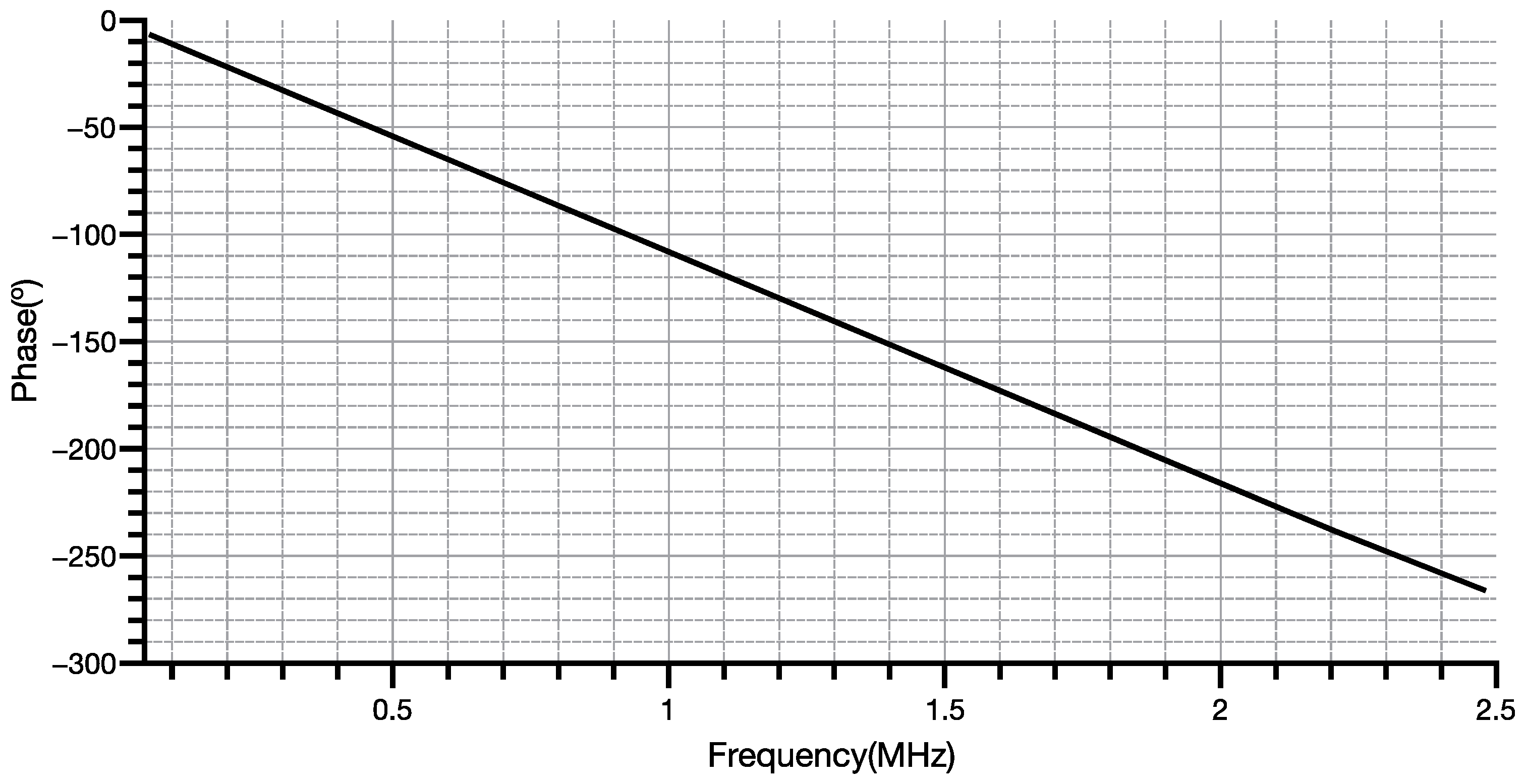
In Figure 11, the phase response of the time-mode low-pass filter is illustrated for a frequency range between 10 kHz and 2.5 MHz. The phase response was measured by employing DFT in the input and output signals of the system, calculating the phase difference described by:
P h a s e ( o ) = θ o u t . f 0 θ i n . f 0
where θin.f0 and θout.f0 are the phases of the input and output signals, respectively. The phase difference between the output and input of the system has a linear relationship with the frequency of the input signal, as is expected by discrete-time system theory. It should be mentioned that, in relation to the phase response of an ideal discrete z-domain low-pass filter, an additional phase difference is added due to the inherent z−1 operation of the time adder. As a result, the proposed system presents a phase difference of −135° at the cut-off frequency instead of −45° of the ideal discrete low-pass filter in which the time adder does not add additional time delay.
Lastly, the summary results of the time-mode z-domain low-pass filter are presented in Table 1.

5. Conclusions

In this work, a first-order low-pass time-mode filter was designed. The filter is constructed using a z−1 operator and a time adder with gain ½. The circuit achieves the desired frequency response, cut-off frequency, and phase response over process and temperature corners. Due to its modular design and the fact that is synchronous with the sampling signal of the system, it can be used as a fundamental building block in the field of time-mode z-domain circuits and systems. As a result, this topology is going to be employed in the implementation of more complex filters suitable for time-mode z-domain signal processing, such as z-domain filters based on bilinear approximation and analog FIR/IIR filters. The implementation of time-mode z-domain filters is an interesting approach because it uses mainly digital standard cells while the analog part is minimized. Hence, it is characterized by low power consumption, high speed, and adaptation of technology scaling, in which the conventional pure analog approach fails [21].

Author Contributions

Conceptualization, K.P.P., O.P.-F. and S.V.; methodology, S.V.; validation, K.P.P.; formal analysis, K.P.P., O.P.-F. and S.V.; investigation, K.P.P., O.P.-F. and S.V.; resources, S.V.; data curation, K.P.P.; writing—original draft preparation, K.P.P. and O.P.-F.; writing—review and editing, S.V.; visualization, K.P.P. and S.V.; supervision, S.V.; project administration, S.V. All authors have read and agreed to the published version of the manuscript.

Funding

This research received no external funding.

Data Availability Statement

Not applicable.

Conflicts of Interest

The authors declare no conflict of interest.

References

  1. Asada, K.; Nakura, T.; Iizuka, T.; Ikeda, M. Time-Domain Approach for Analog Circuits in Deep Sub-Micron LSI. IEICE Electron. Express 2018, 15, 20182001. [Google Scholar] [CrossRef]
  2. Roberts, G.W.; Ali-Bakhshian, M. A Brief Introduction to Time-to-Digital and Digital-to-Time Converters. IEEE Trans. Circuits Syst. II Express Briefs 2010, 57, 153–157. [Google Scholar] [CrossRef]
  3. Lee, D.; Lee, D.; Lee, T.; Kim, Y.H.; Kim, L.S. An Integrated Time Register and Arithmetic Circuit with Combined Operation for Time-Domain Signal Processing. In Proceedings of the 2015 IEEE International Symposium on Circuits and Systems, Lisbon, Portugal, 24–27 May 2015; pp. 1830–1833. [Google Scholar] [CrossRef]
  4. Elgreatly, A.; Dessouki, A.; Mostafa, H.; Abdalla, R.; El-Rabaie, E. A Novel Highly Linear Voltage-to-Time Converter (VTC) Circuit for Time-Based Analog-to-Digital Converters (ADC) Using Body Biasing. Electronics 2020, 9, 2033. [Google Scholar] [CrossRef]
  5. Pekau, H.; Yousif, A.; Haslett, J.W. A CMOS Integrated Linear Voltage-to-Pulse-Delay-Time Converter for Time Based Analog-to-Digital Converters. In Proceedings of the IEEE International Symposium on Circuits and Systems, Kos, Greece, 21–24 May 2006; pp. 2373–2376. [Google Scholar] [CrossRef]
  6. Kwon, H.J.; Lee, J.S.; Kim, B.; Sim, J.Y.; Park, H.J. Analysis of an Open-Loop Time Amplifier with a Time Gain Determined by the Ratio of Bias Current. IEEE Trans. Circuits Syst. II Express Briefs 2014, 61, 481–485. [Google Scholar] [CrossRef]
  7. Yuan, F. Design Techniques of All-Digital Arithmetic Units for Time-Mode Signal Processing. IET Circuits Devices Syst. 2018, 12, 753–763. [Google Scholar] [CrossRef]
  8. Ali-Bakhshian, M.; Roberts, G.W. Digital Storage, Addition and Subtraction of Time-Mode Variables. Electron. Lett. 2011, 47, 910–911. [Google Scholar] [CrossRef]
  9. Panetas-Felouris, O.; Vlassis, S. A 3rd-Order FIR Filter Implementation Based on Time-Mode Signal Processing. Electronics 2022, 11, 902. [Google Scholar] [CrossRef]
  10. Abdelfattah, M.; Roberts, G.W.; Chodavarapu, V.P. All-Digital Time-Mode Elliptic Filters Based on the Operational Simulation of LC Ladders. In Proceedings of the IEEE International Symposium on Circuits and Systems, Melbourne, VIC, Australia, 1–5 June 2014; pp. 2125–2128. [Google Scholar] [CrossRef]
  11. Abdelfattah, M.; Roberts, G.W. All-Digital Time-Mode Direct-Form All-Pole Biquadratic Filter Realization. IEEE Trans. Circuits Syst. II Express Briefs 2017, 64, 1262–1266. [Google Scholar] [CrossRef]
  12. Ali-Bakhshian, M.; Roberts, G.W. A Digital Implementation of a Dual-Path Time-to-Time Integrator. IEEE Trans. Circuits Syst. I Regul. Pap. 2012, 59, 2578–2591. [Google Scholar] [CrossRef]
  13. Karmakar, A.; De Smedt, V.; Leroux, P. Pseudo-Differential Time-Domain Integrator Using Charge-Based Time-Domain Circuits. In Proceedings of the 2021 IEEE 12th Latin America Symposium on Circuits and System (LASCAS), Arequipa, Peru, 21–24 February 2021; IEEE: Piscataway, NJ, USA; pp. 1–4. [Google Scholar]
  14. Park, Y.J.; Jarrett-Amor, D.; Yuan, F. Time Integrator for Mixed-Mode Signal Processing. In Proceedings of the IEEE International Symposium on Circuits and Systems, Montreal, QC, Canada, 22–25 May 2016; pp. 826–829. [Google Scholar] [CrossRef]
  15. Kim, D.; Kim, K.; Yu, W.; Cho, S. A Second-Order ΔΣ Time-to-Digital Converter Using Highly Digital Time-Domain Arithmetic Circuits. IEEE Trans. Circuits Syst. II Express Briefs 2019, 66, 1643–1647. [Google Scholar] [CrossRef]
  16. Yuan, F. CMOS Time-to-Digital Converters for Mixed-Mode Signal Processing. J. Eng. 2014, 2014, 140–154. [Google Scholar] [CrossRef]
  17. Ziabakhsh, S.; Gagnon, G.; Roberts, G.W. A Second-Order Bandpass ΔΣ Time-to-Digital Converter with Negative Time-Mode Feedback. IEEE Trans. Circuits Syst. I Regul. Pap. 2019, 66, 1355–1368. [Google Scholar] [CrossRef]
  18. Razavi, B. The Z-Transform for Analog Designers [The Analog Mind]. IEEE Solid-State Circuits Mag. 2020, 12, 8–14. [Google Scholar] [CrossRef]
  19. Pagkalos, K.P.; Panetas-Felouris, O.; Vlassis, S. Charge-Based Time Registers for z−1 Implementation. In Proceedings of the Panhellenic Conference on Electronics & Telecommunications, Tripolis, Greece, 2–3 December 2022; pp. 1–6. [Google Scholar] [CrossRef]
  20. Panetas-Felouris, O.; Vlassis, S. A Time-Domain Z−1 Circuit with Digital Calibration. J. Low Power Electron. Appl. 2022, 12, 3. [Google Scholar] [CrossRef]
  21. Ravinuthula, V.; Garg, V.; Harris, J.G.; Fortes, J.A.B. Time-Mode Circuits for Analog Computation. Int. J. Circuit Theory Appl. 2009, 37, 631–659. [Google Scholar] [CrossRef]
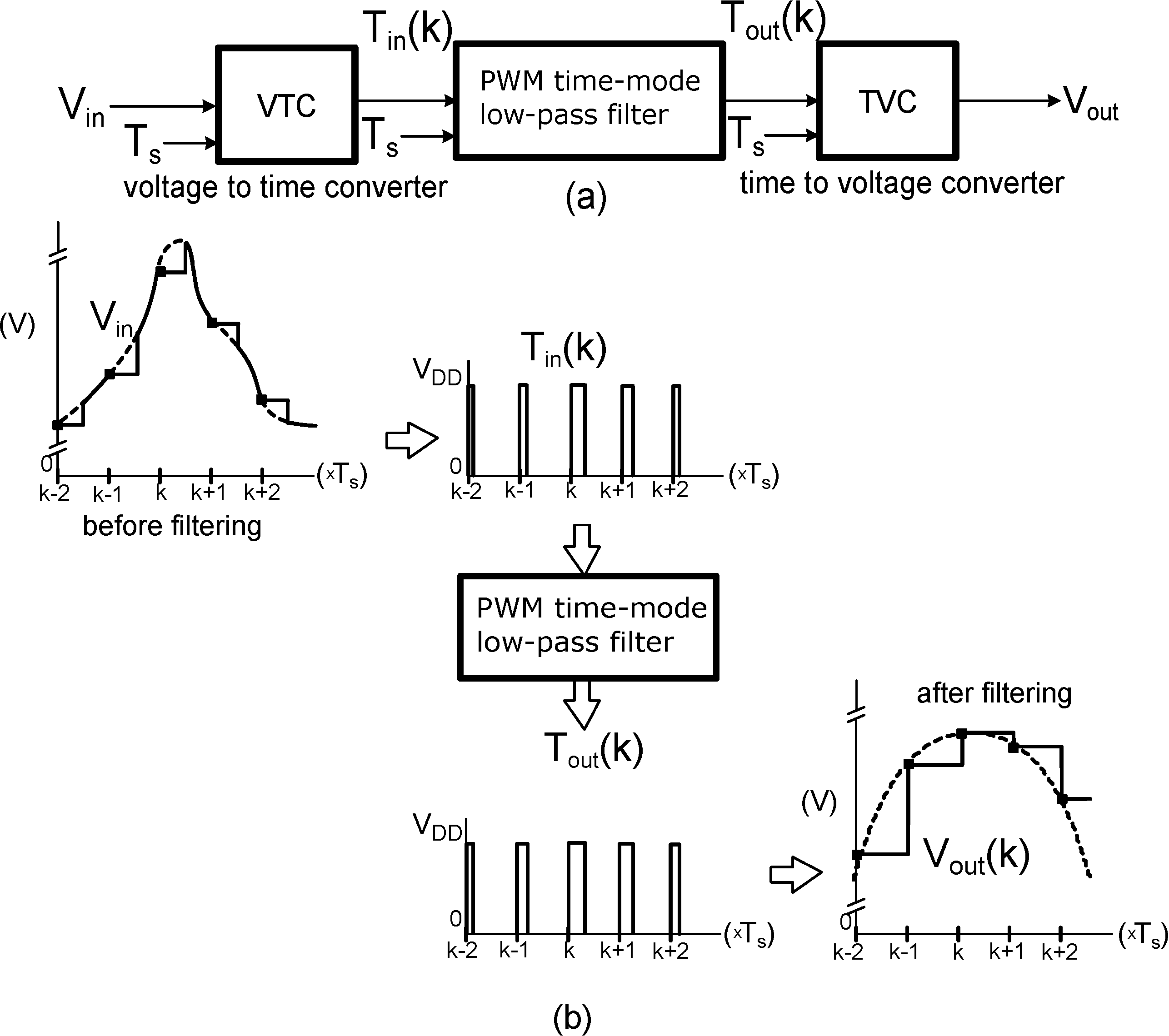
Figure 1. (a) Conceptual system block of the PWM time-mode low-pass filter, (b) Signal flow of the PWM time-mode filter.
Jlpea 13 00032 g001
Figure 2. (a) Top-level topology, (b) circuit architecture, and (c) timing diagram.
Jlpea 13 00032 g002
Figure 3. (a) Intuitive circuit schematic of the gate-controlled time register, (b) timing diagram, and (c) symbol.
Jlpea 13 00032 g003
Figure 4. (a) Implementation of the time-adder core circuit with gain ½, (b) timing diagram, and (c) symbol.
Jlpea 13 00032 g004
Figure 5. (a) Symbol of z−1 operator, (b) architecture with two cascaded time registers, and (c) timing diagram.
Jlpea 13 00032 g005
Figure 6. (a) Symbol of z−1 time-adder with gain ½. (b) architecture with the TADD ½ in series with time register, and (c) timing diagram.
Jlpea 13 00032 g006
Figure 7. Intuitive topology of digital calibration loop.
Jlpea 13 00032 g007
Figure 8. Simulation test bench for the characterization of the time-mode PWM low-pass filter.
Jlpea 13 00032 g008
Figure 9. Input and output transient response of the low-pass filter for frequency 58.59375 kHz.
Jlpea 13 00032 g009
Figure 10. Frequency response of the time-mode low-pass filter over PT corners.
Jlpea 13 00032 g010
Figure 11. Phase response of the time-mode low-pass filter.
Jlpea 13 00032 g011
Table 1. Summary results of the first-order time-mode low-pass filter.
UnitsMin.Typ.Max.
FsamplingMHz5
Gain @ 58.59 kHzdB−0.045−0.0310.106
fcut.offMHz1.22731.23231.2352
Power ConsumptionμW59.04
Disclaimer/Publisher’s Note: The statements, opinions and data contained in all publications are solely those of the individual author(s) and contributor(s) and not of MDPI and/or the editor(s). MDPI and/or the editor(s) disclaim responsibility for any injury to people or property resulting from any ideas, methods, instructions or products referred to in the content.