Article

Ocelli: Efficient Processing-in-Pixel Array Enabling Edge Inference of Ternary Neural Networks

1
School of Computing, University of Nebraska-Lincoln, Lincoln, NE 68588, USA
2
Department of Electrical and Computer Engineering, New Jersey Institute of Technology, Newark, NJ 07102, USA
*
Authors to whom correspondence should be addressed.
J. Low Power Electron. Appl. 2022, 12(4), 57; https://doi.org/10.3390/jlpea12040057
Submission received: 28 September 2022 / Revised: 20 October 2022 / Accepted: 27 October 2022 / Published: 30 October 2022
(This article belongs to the Special Issue Low-Power Computation at the Edge)

Abstract

:
Convolutional Neural Networks (CNNs), due to their recent successes, have gained lots of attention in various vision-based applications. They have proven to produce incredible results, especially on big data, that require high processing demands. However, CNN processing demands have limited their usage in embedded edge devices with constrained energy budgets and hardware. This paper proposes an efficient new architecture, namely Ocelli includes a ternary compute pixel (TCP) consisting of a CMOS-based pixel and a compute add-on. The proposed Ocelli architecture offers several features; (I) Because of the compute add-on, TCPs can produce ternary values (i.e., −1, 0, +1) regarding the light intensity as pixels’ inputs; (II) Ocelli realizes analog convolutions enabling low-precision ternary weight neural networks. Since the first layer’s convolution operations are the performance bottleneck of accelerators, Ocelli mitigates the overhead of analog buffers and analog-to-digital converters. Moreover, our design supports a zero-skipping scheme to further power reduction; (III) Ocelli exploits non-volatile magnetic RAMs to store CNN’s weights, which remarkably reduces the static power consumption; and finally, (IV) Ocelli has two modes, including sensing and processing. Once the object is detected, the architecture switches to the typical sensing mode to capture the image. Compared to the conventional pixels, it achieves an average 10% efficiency on its lane detection power consumption compared with existing edge detection algorithms. Moreover, considering different CNN workloads, our design shows more than 23% power efficiency over conventional designs, while it can achieve better accuracy.

1. Introduction

Internet of Things (IoT) devices are projected to attain an $1100B market by 2025 [1]. Energy harvesting systems (EHSs) and wireless sensor networks (WSNs) with ambient energy sources and low maintenance have impacted a wide range of IoT applications such as wearable devices, agriculture, smart cities, and many more, while in scene interpretation, IoT nodes include sensory systems enabling massive data collection from the environment and people to process with on-/off-chip processors ( 10 18 bytes/s or ops). These emerging systems require both continuous sensing and instant processing. Nonetheless, the high energy data conversion/transmission of raw data and the limited available energy from ambient energy sources make designing energy-efficient and low bandwidth CMOS vision sensors challenging. Moreover, even using low-power sensors to realize artificial intelligence tasks such as object detection faces serious challenges for their tractability in computational and storage resources. Effective techniques in both software and hardware domains have been developed to improve CNN efficiency by alleviating the “power and memory wall” bottleneck.
In algorithm-based approaches, the use of shallower but wider CNN models, quantizing parameters, and low-precision computing has been explored thoroughly [2,3,4]. From the hardware point of view, the underlying operations should be realized using efficient mechanisms such as beyond CMOS technology nodes, and non-Von Neumann architectures [5,6,7]. This paves the way for new sensor paradigms such as processing-near-sensor (PNS), processing-in-sensor (PIS), and processing-in-pixel (PIP), where digital outputs of a pixel are accelerated near/in the sensor. The vision sensors’ processing energy has been reduced significantly, from 0.1 pJ/OP to 1 pJ/OP, by leveraging these methods. Besides, a remarkable reduction in off-chip data transfer energy has been reported. In addition to reducing the processing power, the sensing part should be optimally designed, enabling an acceptable accuracy.

2. Near/In-Sensor Processing Background

Systematic integration of computing and sensor arrays has been widely studied to eliminate off-chip data transmission and reduce ADC bandwidth by combining CMOS image sensors and processors in one chip, known as PNS [8,9,10,11,12], or even integrating pixels and computation unit so-called PIS [13,14,15,16]. In [9], photocurrents are transformed into pulse-width modulation signals, and a dedicated analog processor is designed to execute feature extraction reducing ADC power consumption. In [17], 3D-stacked column-parallel ADCs and Processing Elements (PE) are implemented to run spatiotemporal image processing. In [18], a CMOS image sensor with dual-mode delta-sigma ADCs is designed to process 1st-conv, layer of binarized-weight neural networks (BWNN). RedEye [6] executes the convolution operation using charge-sharing tunable capacitors. Although this design shows energy reduction compared to a CPU/GPU by sacrificing accuracy, to achieve high accuracy computation, the required energy per frame increases dramatically by 100×. MACSEN [5] as a PIS platform processes the 1st-conv. layer of BWNNs with the correlated double sampling procedure achieving 1000 fps speed in computation mode. However, it suffers from humongous area-overhead and power consumption mainly due to the SRAM-based PIS method. In [19], a pulse-domain algorithm uses fundamental building blocks, photodiode arrays, and an ADC to perform near-sensor image processing that reduces design complexity and enhances both cost and speed. Finally, the PIP scheme allows simultaneous sensing and computing. Thus, several works accelerated the first layers using PIP architecture and submitted the rest to the digital neural network accelerator [20,21]. Putting all together, there are three main bottlenecks in IoT imaging systems that this work explores and aims to solve: (1) the conversion and storage of pixel values consume most of the power (>96% [22]) in conventional image sensors; (2) the computation imposes a large area-overhead and power consumption in more recent PNS/PIS units and requires extra memory for intermediate data storage; and (3) the system is hardwired so the functionality is limited to simple pre-processing tasks such as 1st-layer BWNN computation and cannot go beyond that.

3. Proposed Ternary Compute Pixel

Figure 1a depicts a possible high-performance and energy-efficient architecture enabling machine learning tasks for edge devices. It consists of an m × n Compute Focal Plane (CFP) array, row and column controllers (Ctrl), command decoder, sensor timing Ctrl, and sensor I/O operating in two modes, i.e., sensing and processing. The CFP is designed to co-integrate sensing and processing of the 1st-layer of ternary weight neural network (TWNN), targeting a low-power but high classification accuracy. Because the first layer’s convolution operations are the performance bottleneck of almost all hardware/software co-design accelerators [23], the proposed Ocelli is introduced as a promising solution to efficiently perform computation and sensing for the first layer of NNs. To further accelerate, the output of the first layer is transmitted to an on-chip deep learning accelerator unit to compute the remaining TWNN layers. Designing a domain-specific accelerator is out of scope. Once the object is roughly detected, the architecture switches to the sensing mode like a traditional rolling-shutter CMOS image sensor. In order to enable an integrated sensing and processing mode, a conventional 4T-pixel is upgraded to a ternary compute pixel (TCP), which is composed of a pixel, including five transistors and one photodiode (PD), and compute add-ons (CAs) as shown in Figure 1b. The compute add-on includes three transistors, where T6 and T7 operate as deep triode region current sources and a 2:1 multiplexer (MUX) controlled by a non-volatile memory (NVM) element. There are two common signals among TCPs, RowIndex ( R i ) and ComputeRow (CR) signals. The R i signal is controlled by Row Ctrl and shared across pixels located in the same row to enable access during the row-wise sensing mode. However, the CR is a unique, controlling signal connected to entire TCP units activated during processing mode. A sense bit-line (SBL) is shared across the pixels on the same column connected to sensor peripherals for integrated sensing-processing mode. Moreover, TCPs share s compute bit-lines (CBLs), each connected to a sense amplifier for processing. The 1st-layer ternary weights (i.e., −1, 0, +1) corresponding to each pixel is pre-stored into NVMs based on Equation (1), where w i denotes the full precision weight tensor, w i is the weight after quantization, and Δ th is symmetric threshold [3]:
w i = 1 × s i g n ( w i ) | w i | Δ th 0 | w i | < Δ th
We selected STT-MRAM [24] as the NVM unit using parameters listed in Table 1, depicted in Figure 1b. The binary data is stored as the magnetization direction in the MTJ’s free layer, which could be programmed through the current-induced STT by NVM write driver. A reference resistor is then used to realize a voltage divider circuit to read out the weight value from memory. Although STT-MRAM provides interesting features such as near-zero standby power and high integration density, it can be replaced by other NVM technologies. Due to the high write power of STT-MRAM, the network weights are written once and then leveraged during the inference phase without any update.
The TCP has one more transistor (T1) than the conventional 4T-pixel, which is connected to the enable (En) signal. This extra transistor supports a zero-skipping scheme that can enable/disable TCPs. If the weight is zero, the TCP is OFF, considered an ineffective pixel, and its capacitor does not charge, resulting in a significant power saving. The effectiveness of this approach is demonstrated by applying it to the neural networks with quantized weights, especially in extremely high sparsity ratios (e.g., 95%), such as BWNNs and TWNNs. It is worth mentioning that for a wide variety of image processing tasks such as sharpening, edge detection, and smoothing, they can be readily implemented within a TCP due to their simple filters (masks). In TCP architecture, to create positive and negative currents, the drains of T6 and T7 are connected to V D D and − V D D / 3 , respectively. After exposure, the set of input sensor voltages ( V P D ) is applied to the gates of T6, generating a current set on the C B L s lines. If the binary value equals ‘1’ ( w i = + 1 ), T6 acts as a current source and generates a positive current on the shared C B L , shown by the red dashed line in Figure 1b. However, if the binary value equals ‘0’ ( w i = 1 ), T7 produces the same current magnitude but in the opposite direction, indicated by the blue dashed line shown in Figure 1b. The generated currents directly correlate with the input’s intensity (voltage value of C P D ). By leveraging this mechanism, every input pixel value is converted to a weighted current according to the NVM, and E n is interpreted as the multiplication in TWNNs. Then, by disabling T1, values of T6 and T7 gates will be completely discharged to zero, which means none of the transistors can produce current. More pixels with even non-zero weights can be turned off to save more power at the cost of accuracy degradation. If E n = 0 , the TCP turns on, and it can operate in one of the two sensing or processing modes.

3.1. Sensing Mode

In the sensing mode, initially setting R s t = ‘high’, the PD connected to the T2 transistor turns into inverse polarization. In this way, turning on the access transistor T4 and k 1 switch at the shared ADC (Figure 1c) allows the C 1 capacitor to charge through S B L fully. By turning off T2, PD generates a photo-current concerning the external light intensity, which in turn leads to a voltage drop ( V P D ) at the gate of T3. Once again, by turning on T4 and this time k 2 switch, C 2 is selected to record the voltage drop. Therefore, the voltage values before and after the image light exposure, i.e., V 1 and V 2 in Figure 1c, are sampled. The difference between two voltages is sensed with an amplifier, while this value is proportional to the voltage drop on V P D . In other words, the voltage at the cathode of PD can be read at the pixel output. Throughout the sensing mode, the C R signal is grounded. Reading the pixels’ values in the sensing mode is performed in a row-by-row manner; therefore, reading all pixels requires r clock cycles, where r is the number of rows. Figure 2a depicts the sensing mode, where the first row and n columns are selected and connected to the dedicated ADCs.

3.2. Processing Mode

Figure 2b shows a selected r × 1 TCP array. In the processing mode, the C P D capacitor is initialized to the fully-charged state by setting R s t = ‘high’, similar to the sensing mode. During an evaluation cycle, by turning off T1, T2, and T3, the Row Ctrl activates the C R signal while the R i signals are deactivated. This activates the entire array for a single-cycle multiply-accumulate operation. In this mode, the CA is utilized to leverage pixel’s V P D as a sampling voltage in s-NVM units to simultaneously generate (/pull) current through T6 (/T7) on the C B L . To implement multiplications between the pixel value identified by V P D and the binary weight stored in NVM, a 2:1 MUX unit is devised in every TCP, taking the T6s and T7 source signals as inputs and NVM sensed data as the selector.
Although NVM elements can only store binary values, i.e., ‘0’ and ‘1’, the proposed Ocelli is able to produce ternary values. To do so, first, the absolute values of pre-trained weights ( w i ) are connected to the E n signal; the NVM components are then filled by ‘0’ and ‘1’ to denote weights −1 and +1, respectively. Table 2 summarizes the CA output based on the E n signal and NVM value where β is the β ratio of the transistors. Due to the specific features of STT-MRAM, the Ocelli obtains a high speed, reliability, and low power consumption in processing mode compared to previous designs. It is noteworthy that the TCP can disconnect PD using T5 to stop discharging C P D and freeze the pixel value. Then, the values are read in a row-by-row manner, and because of preventing unnecessary C P D discharge, power consumption reduces, and better-quality images might be captured. The current flow of each transistor is measured using Equation (2) based on the transistors’ working regions:
i D = K n v g s V T 2 i D = K n 2 ( v g s V T ) v d s v d s 2
K n = 1 / 2 μ n C o x W / L
where v g s ( v d s ) is the voltage between of gate and source (drain and source), V T is the threshold voltage, and K n is MOSFET transconductance. The MOSFET transconductance is determined by the manufacturing process and calculated based on Equation (3), where μ n is the mobility of electrons at the surface of the channel, C o x is oxide capacitance, and W and L are width and length of the chancel, respectively. According to the equations, the current flow of the transistors has a direct relation with v g s and K n . In the proposed design, T6 and T7 have different v g s voltages. Therefore, to produce approximately the same current using T6 and T7, we change the width of the transistors based on Equation (3). In this paper, we define β regarding transistors’ parameters to produce the same current in both transistors.
The developed sense amplifier, shown in Figure 1d and Figure 2b, requires two clock phases: pre-charge (Clk ‘high’) and sensing (Clk ‘low’). The summation current corresponding to V P D s, on CBL, is converted to the voltage ( V s e n s e ) at the input of the sense amplifier. This voltage is compared with the reference voltage by applying a proportional current over a processing reference resistor ( R p r o ) activated by the mode signal, as shown in Figure 1d. In our design, the sense amplifier output ( V o u t ) sets to 0 for values lower than ‘0’ and sets to 1 for higher than ‘0’. According to Kirchhoff’s law, the multiplications of MACs are performed using the conductance of the nodes consisting of the weights and the generated voltages based on the input light intensities, while the accumulation is done by summing the currents. Note that T6’s and T7’s gate capacitors, as well as parasitic capacitors, will be fully charged to V D D through T1 and T2 in the pre-charge cycle; this will significantly keep the pixel sensitivity high when the number of CAs increases.

4. Simulation Results

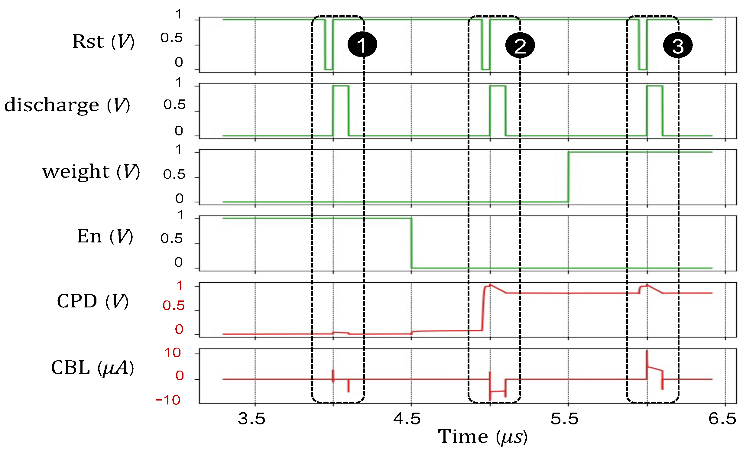
In this paper, simulations are conducted using the HSpice simulator for a 45 nm PTM low power metal gate at room temperature (25 °C). Figure 3 shows the functionality of one TCP. In this figure, as shown in ❶, when E n equals V D D , V P D is never charged, and the produced current on C B L is approximately zero. On the other hand, in ❷, by changing the E N value to zero, with the first R s t clock (0), CPD is charged to V D D , and when R s t is returned to 1 again, and d i s c h a r g e is V D D , C P D start discharging. At the end of ❷, the value of the V P D has remained the same. Everything in ❸ is similar to ❷ except the weight values. Before starting the sensing and processing phases, the pre-trained weights should be written into NVMs and remain unchanged in the TCPs. Nevertheless, to evaluate the output current, we changed the TCP weights. This simulation indicates TCP with negative and positive weights produces a current value of approximately −5 μA and +5 μA, respectively.
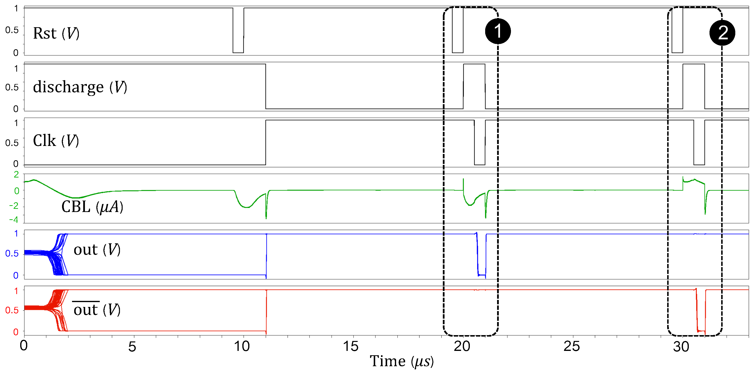
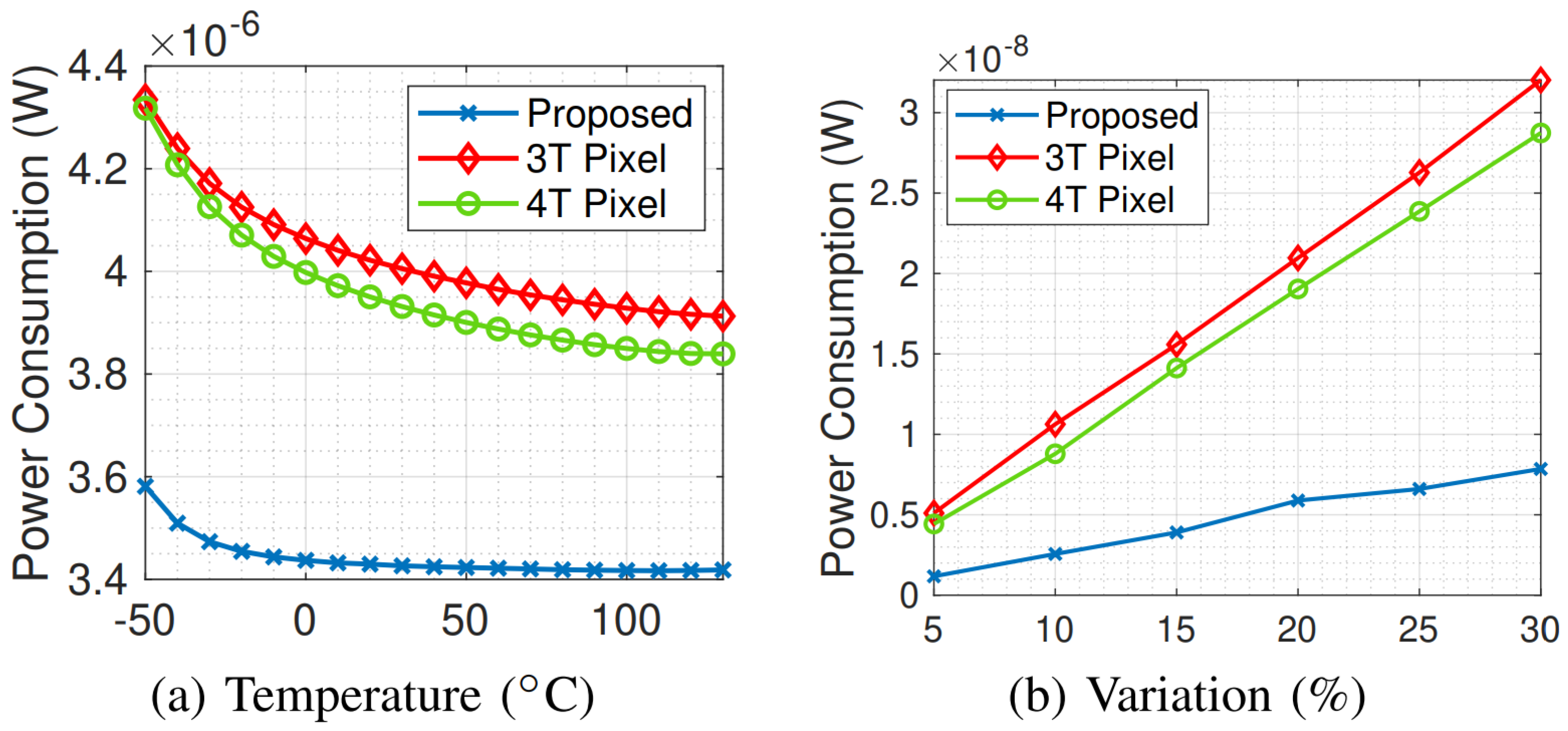
The transient simulation results of an 8 × 1 TCP array are shown in Figure 4. Herein, eight TCPs are connected to the C B L . The results are obtained in the presence of 15% process variation in transistor sizing for 1000 simulation runs. Furthermore, the proposed pixel simulates various situations, including temperature and mismatching of both capacitor and transistor sizes. As shown in Figure 5a,b, the proposed design is more resilient in both situations. To verify Ocelli’s functionalities, the evaluation phase can be divided into two phases. In phase ❶, some sensors were disabled. Therefore, the sum of the current according to their weight becomes approximately 1 μ A in the evaluation phase at the rising edge of the Clk signal. As previously mentioned, the current value smaller than 0 interprets as ‘0’, and bigger than 0 denotes as ‘1’. Therefore in ❶, the output of the SA (out) is 0, whereas, in ❷, the weights changed and generated a positive current, and out became 1. As depicted in Figure 4, the proposed pixel is resilient during the process variation, and all waveforms approximately have the same value in each iteration.

Comparison Results

We demonstrate the advantages of the Ocelli design through an application-level evaluation. Regarding edge detection techniques, although the Soble mask is the most widely used algorithm, implementing two 3 × 3 matrices, the X-direction and the Y-direction, consisting of five different weights { 2 , 1 , 2 } is challenging. Thus, in our study, three energy-efficient filters are considered: the Prewitt (two 3 × 3 matrices), the Roberts (two 2 × 2 matrices), and the Column-Comparing (CC) technique (one 2 × 2 matrix) including { 1 , 0 , 1 } weights [25]. Figure 6 illustrates the power consumption results for three sensors after the masks have been applied. As a first observation, the simpler a mask is, the less accurate the results, and correspondingly, the less power is consumed. The CC mask is the smallest and simplest one that shows power efficiency at the cost of lower accuracy.
In this study, Pratt’s figure of merit (PFOM) [26] is used in order to analyze the accuracy of the edge detected images since determining their accuracy is difficult. In PFOM, a comparison is conducted between the detected edges and the ideal image to determine how many pixels are different. Therefore, the closer the PFOM (%) comes to 100, the more ideal it is. Here the Sobel mask is considered as a baseline because it is the most highly-used one for diagonal detection [27].
The second observation is that the proposed Ocelli shows the most optimal results due to its zero-skipping and ternary weights. We obtained our results based on a grayscale image of 240 × 160 with a stride of 1 and padding of 0. We demonstrate the advantages of the proposed design through various NN workloads. Since these modern workloads have different degrees of weight sparsity ratio, from 60% to 90% [23], developing an efficient and promising approach is vital but challenging. Table 3 illustrates three various application domains, which cover a wide range of machine learning models. To make a fair comparison, three PIP designs, including 3T and 4T-pixels, and the proposed TCP are considered. The first two architectures can implement BWNNs (−1, +1), while our TCP implements TWNN (−1, 0, +1). After performing the first layer’s computations, the remaining layers can be accelerated with an identical NN accelerator. The obtained power-normalized results considering the first layers are summarized in Table 3. The results show that the Ocelli architecture provides better power efficiency while higher accuracy can be achieved rather than BWNNs based on 3T and 4T-pixels [3]. This improvement is because of the zero-skipping technique realized by the TCP. It is worth noting that we can alter BWNNs’ values from (−1, +1) to (0, +1), which causes several issues like no guarantee for convergence.

5. Conclusions

This paper proposed an efficient processing-in-pixel approach enabling edge inference. The proposed Ocelli architecture provides ternary values that realize low-precision TWNNs at the cost of a small area overhead. The proposed Ocelli targets the first layer of NNs to significantly reduce the overhead of analog buffers and analog-to-digital converters. Moreover, it supports the zero-skipping technique, vital for evolving DNN models. The Ocelli design achieves better performance than a BWNN using conventional 3T and 4T -pixels, while it can show better accuracy due to its higher precision.

Author Contributions

Investigation, S.T. and S.A.; Methodology, S.T.; Supervision, A.R.; Visualization, A.R.; Writing—original draft, S.T.; Writing—review & editing, S.A. and A.R. All authors have read and agreed to the published version of the manuscript.

Funding

This work is supported in part by the National Science Foundation under Grant No. 2216772, 2216773 and 2228028.

Data Availability Statement

Not applicable.

Conflicts of Interest

The authors declare no conflict of interest.

References

  1. Hsu, T.H.; Chiu, Y.C.; Wei, W.C.; Lo, Y.C.; Lo, C.C.; Liu, R.S.; Tang, K.T.; Chang, M.F.; Hsieh, C.C. AI edge devices using computing-in-memory and processing-in-sensor: From system to device. In Proceedings of the 2019 IEEE International Electron Devices Meeting (IEDM), San Francisco, CA, USA, 7–11 December 2019; IEEE: Piscataway, NJ, USA, 2019; pp. 22.5.1–22.5.4. [Google Scholar]
  2. Rastegari, M.; Ordonez, V.; Redmon, J.; Farhadi, A. Xnor-net: Imagenet classification using binary convolutional neural networks. In Proceedings of the European Conference on Computer Vision, Amsterdam, The Netherlands, 8–16 October 2016; Springer: Berlin/Heidelberg, Germany, 2016; pp. 525–542. [Google Scholar]
  3. Zhu, C.; Han, S.; Mao, H.; Dally, W.J. Trained Ternary Quantization. In Proceedings of the International Conference on Learning Representations (ICLR) 2017, Toulon, France, 24–26 April 2017. [Google Scholar]
  4. Zhou, S.; Wu, Y.; Ni, Z.; Zhou, X.; Wen, H.; Zou, Y. DoReFa-Net: Training low bitwidth convolutional neural networks with low bitwidth gradients. arXiv 2016, arXiv:1606.06160. [Google Scholar]
  5. Xu, H.; Li, Z.; Lin, N.; Wei, Q.; Qiao, F.; Yin, X.; Yang, H. Macsen: A processing-in-sensor architecture integrating mac operations into image sensor for ultra-low-power bnn-based intelligent visual perception. IEEE Trans. Circuits Syst. II Express Briefs 2020, 68, 627–631. [Google Scholar] [CrossRef]
  6. LiKamWa, R.; Hou, Y.; Gao, J.; Polansky, M.; Zhong, L. Redeye: Analog convnet image sensor architecture for continuous mobile vision. ACM SIGARCH Comput. Archit. News 2016, 44, 255–266. [Google Scholar] [CrossRef]
  7. Xu, H.; Lin, N.; Luo, L.; Wei, Q.; Wang, R.; Zhuo, C.; Yin, X.; Qiao, F.; Yang, H. Senputing: An Ultra-Low-Power Always-On Vision Perception Chip Featuring the Deep Fusion of Sensing and Computing. IEEE Trans. Circuits Syst. I Regul. Pap. 2021, 69, 232–243. [Google Scholar] [CrossRef]
  8. Li, Q.; Liu, C.; Dong, P.; Zhang, Y.; Li, T.; Lin, S.; Yang, M.; Qiao, F.; Wang, Y.; Luo, L.; et al. NS-FDN: Near-Sensor Processing Architecture of Feature-Configurable Distributed Network for Beyond-Real-Time Always-on Keyword Spotting. IEEE Trans. Circuits Syst. I Regul. Pap. 2021, 68, 1892–1905. [Google Scholar] [CrossRef]
  9. Hsu, T.H.; Chen, Y.R.; Liu, R.S.; Lo, C.C.; Tang, K.T.; Chang, M.F.; Hsieh, C.C. A 0.5-V Real-Time Computational CMOS Image Sensor with Programmable Kernel for Feature Extraction. IEEE J. Solid-State Circuits 2020, 56, 1588–1596. [Google Scholar] [CrossRef]
  10. Bhowmik, P.; Pantho, M.J.H.; Bobda, C. Visual cortex inspired pixel-level re-configurable processors for smart image sensors. In Proceedings of the 2019 56th ACM/IEEE Design Automation Conference (DAC), Las Vegas, NV, USA, 2–6 June 2019; IEEE: Piscataway, NJ, USA, 2019; pp. 1–2. [Google Scholar]
  11. Angizi, S.; Morsali, M.; Tabrizchi, S.; Roohi, A. A Near-Sensor Processing Accelerator for Approximate Local Binary Pattern Networks. arXiv 2022, arXiv:2210.06698. [Google Scholar]
  12. Angizi, S.; Roohi, A. Integrated Sensing and Computing using Energy-Efficient Magnetic Synapses. In Proceedings of the 2022 23rd International Symposium on Quality Electronic Design (ISQED), Santa Clara, CA, USA, 6–7 April 2022; IEEE: Piscataway, NJ, USA, 2022; pp. 1–4. [Google Scholar]
  13. Xu, H.; Nazhamaiti, M.; Liu, Y.; Qiao, F.; Wei, Q.; Liu, X.; Yang, H. Utilizing direct photocurrent computation and 2D kernel scheduling to improve in-sensor-processing efficiency. In Proceedings of the 2020 57th ACM/IEEE Design Automation Conference (DAC), San Francisco, CA, USA, 20–24 July 2020; IEEE: Piscataway, NJ, USA, 2020; pp. 1–6. [Google Scholar]
  14. Xu, H.; Liu, Z.; Li, Z.; Ren, E.; Nazhamati, M.; Qiao, F.; Luo, L.; Wei, Q.; Liu, X.; Yang, H. A 4.57 μW@ 120fps Vision System of Sensing with Computing for BNN-Based Perception Applications. In Proceedings of the 2021 IEEE Asian Solid-State Circuits Conference (A-SSCC), Busan, Korea, 7–10 November 2021; IEEE: Piscataway, NJ, USA, 2021; pp. 1–3. [Google Scholar]
  15. Abedin, M.; Roohi, A.; Liehr, M.; Cady, N.; Angizi, S. MR-PIPA: An Integrated Multi-level RRAM (HfO x) based Processing-In-Pixel Accelerator. IEEE J. Explor.-Solid-State Comput. Devices Circuits 2022, 1. [Google Scholar] [CrossRef]
  16. Angizi, S.; Tabrizchi, S.; Roohi, A. Pisa: A binary-weight processing-in-sensor accelerator for edge image processing. arXiv 2022, arXiv:2202.09035. [Google Scholar]
  17. Yamazaki, T.; Katayama, H.; Uehara, S.; Nose, A.; Kobayashi, M.; Shida, S.; Odahara, M.; Takamiya, K.; Hisamatsu, Y.; Matsumoto, S.; et al. 4.9 A 1ms high-speed vision chip with 3D-stacked 140GOPS column-parallel PEs for spatio-temporal image processing. In Proceedings of the 2017 IEEE International Solid-State Circuits Conference (ISSCC), San Francisco, CA, USA, 5–9 February 2017; IEEE: Piscataway, NJ, USA, 2017; pp. 82–83. [Google Scholar]
  18. Kim, W.T.; Lee, H.; Kim, J.G.; Lee, B.G. An on-chip binary-weight convolution CMOS image sensor for neural networks. IEEE Trans. Ind. Electron. 2020, 68, 7567–7576. [Google Scholar] [CrossRef]
  19. Taherian, F.; Asemani, D. Design and implementation of digital image processing techniques in pulse-domain. In Proceedings of the 2010 IEEE Asia Pacific Conference on Circuits and Systems, Kuala Lumpur, Malaysia, 6–9 December 2010; IEEE: Piscataway, NJ, USA, 2010; pp. 895–898. [Google Scholar]
  20. Tabrizchi, S.; Angizi, S.; Roohi, A. TizBin: A Low-Power Image Sensor with Event and Object Detection Using Efficient Processing-in-Pixel Schemes. In Proceedings of the 2022 IEEE International Conference on Computer Design (ICCD), Lake Tahoe, NV, USA, 23–26 October 2022. [Google Scholar]
  21. Song, R.; Huang, K.; Wang, Z.; Shen, H. A reconfigurable convolution-in-pixel cmos image sensor architecture. IEEE Trans. Circuits Syst. Video Technol. 2022, 32, 7212–7225. [Google Scholar] [CrossRef]
  22. Choi, J.; Park, S.; Cho, J.; Yoon, E. An energy/illumination-adaptive CMOS image sensor with reconfigurable modes of operations. IEEE J. Solid-State Circuits 2015, 50, 1438–1450. [Google Scholar] [CrossRef]
  23. Muñoz-Martínez, F.; Abellán, J.L.; Acacio, M.E.; Krishna, T. STONNE: Enabling Cycle-Level Microarchitectural Simulation for DNN Inference Accelerators. In Proceedings of the 2021 IEEE International Symposium on Workload Characterization (IISWC), Storrs, CT, USA, 7–9 November 2021; pp. 201–213. [Google Scholar]
  24. Huai, Y. Spin-transfer torque MRAM (STT-MRAM): Challenges and prospects. AAPPS Bull. 2008, 18, 33–40. [Google Scholar]
  25. Jin, M.; Noh, H.; Song, M.; Kim, S.Y. Design of an edge-detection cmos image sensor with built-in mask circuits. Sensors 2020, 20, 3649. [Google Scholar] [CrossRef] [PubMed]
  26. Abdou, I.E.; Pratt, W.K. Quantitative design and evaluation of enhancement/thresholding edge detectors. Proc. IEEE 1979, 67, 753–763. [Google Scholar] [CrossRef]
  27. Biswas, R.; Sil, J. An improved canny edge detection algorithm based on type-2 fuzzy sets. Procedia Technol. 2012, 4, 820–824. [Google Scholar] [CrossRef] [Green Version]
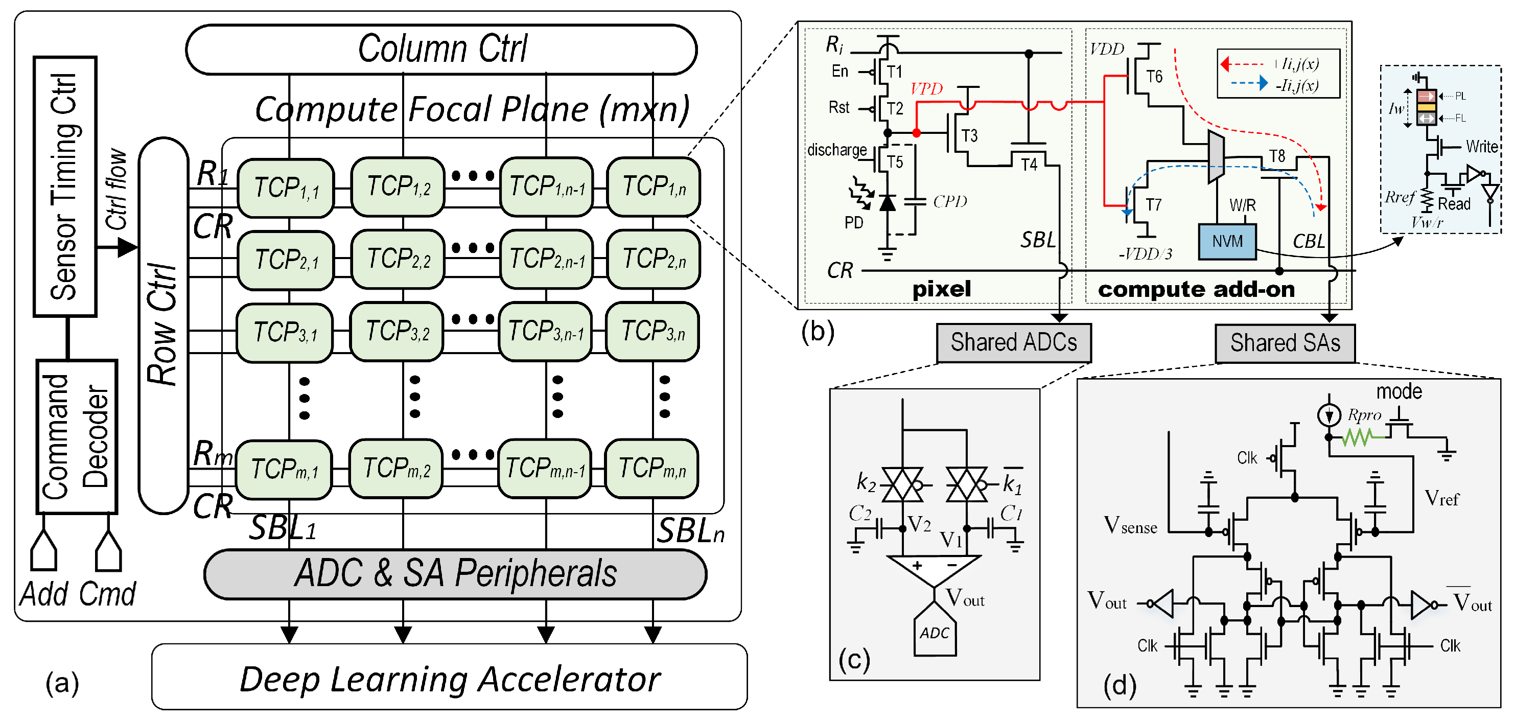
Figure 1. (a) The general Ocelli architecture consists of an m × n TCP array. (b) The proposed TCP includes a pixel and a CA, shared (c) ADCs, and (d) sense amplifier designs.
Jlpea 12 00057 g001
Figure 2. Ocelli’s functionalities in two modes. (a) The sensing mode for a 1 × n TCP array and (b) the processing mode for a m × 1 TCP array.
Jlpea 12 00057 g002
Figure 3. Transient simulation waveform of a TCP with a single CA.
Jlpea 12 00057 g003
Figure 4. Transient simulation waveform of an 8 × 1 TCP array.
Jlpea 12 00057 g004
Figure 5. Relationship between the power consumption and two factors, (a) temperature, and (b) process variation.
Jlpea 12 00057 g005
Figure 6. The obtained images, accuracy, and power consumption results using the examined pixels by applying the three low-cost mask algorithms.
Jlpea 12 00057 g006
Table 1. Simulation Parameters of STT-MTJ.
ParameterDescriptionValue
AreaMTJ Surface100 × 65 × π / 4 nm 2
Reference MTJ Surface100 × 45 × π / 4 nm 3
t o x Thickness of oxide barrier0.85 nm
α Gilbert Damping factor0.007
t f r e e Thickness of free layer1.3 nm
μ B Bohr Magneton9.27e 24 J·T 1
PPolarization (DWNM, MTJ)0.75, 0.5
M s Saturation magnetization200 8e 5 A·m 1
IC0Threshold Current Densitye 10 –e 12 A·m 2
R A P , R P MTJ-1/MTJ-2 Resistance2.5 K Ω , 1.25 K Ω
R p Reference MTJ Resistance1.8 K Ω
TMRTMR ratio100%
H k Out of Plane Anisotropy Field1600∼1800 Oe
k u Uniaxial Anisotropy400e 3 J/m 3
Table 2. Provided currents by a CA regarding E n signal and the stored weights.
Enable Bit
(En)
Stored
NVM Value
Represented
Weight
Output
Current
1x00
00−1 C P D × β
011 C P D × β
Table 3. Normalized power consumption of the first layers for different highly-used CNN models.
DomainDNN Model [23]Power Consumption (1st Layer)
Ocelli (TCP)3T-Pixel4T-Pixel
Image ClassificationMobileNets11.251.21
SqueezeNet11.231.19
AlexNet11.261.22
ResNet-5011.301.26
VGG-1611.311.27
Object DetectionSDD-MobileNets11.251.21
Publisher’s Note: MDPI stays neutral with regard to jurisdictional claims in published maps and institutional affiliations.