3.1. The Effect of C Doping Concentration on the Breakdown Characteristics of cGaN Buffer
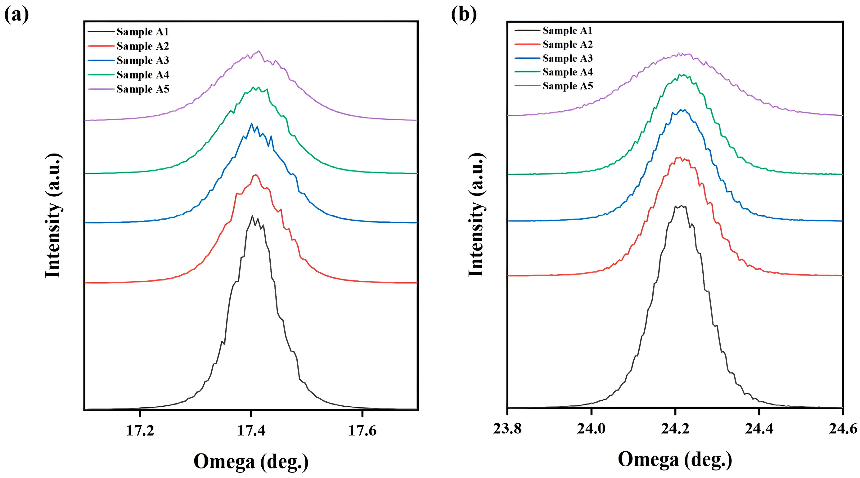
To systematically evaluate the impact of C doping concentration on the crystal quality of GaN buffer layers, we performed HRXRD measurements on all samples as shown in
Figure 3. The FWHM values of (002) and (102) reflections serve as integral indicators of the crystalline quality, as they can be influenced by various factors including dislocations, point defects, and local strain variations. Threading dislocation densities were approximately estimated from the rocking-curve FWHM values measured by HRXRD. According to the GaN-specific methodology summarized by Moram and Vickers [
25], the symmetric (002) reflection of c-plane GaN is mainly sensitive to screw-type threading dislocations, while the asymmetric (102) reflection is more suitable for evaluating edge-type threading dislocations. In this work, the dislocation density was calculated using the relation proposed by Kurtz et al. [
26] for a random dislocation distribution as shown in Equation (1):
Thus, the screw and edge type threading dislocation densities were estimated as
The
ρscrew and
ρedge are the density of screw and edge dislocations, respectively;
β(002) and
β(102) are the FWHM values of the rocking curves for the corresponding crystal planes (converted to radians);
bscrew = <0001> (magnitude of 0.5185 nm) and
bedge = <1120> (magnitude of 0.3189 nm) are the Burgers vectors of screw and edge dislocations in wurtzite GaN, respectively. This method has been proven to be applicable to various GaN heteroepitaxial systems including GaN-on-sapphire, and is a reliable method for dislocation density characterization of GaN epitaxial films [
27,
28].
Since the rocking-curve broadening may also arise from other defects and strain fluctuations, the obtained value should be regarded as an approximate indicator of crystalline quality rather than a strictly exact dislocation density in our research.
Table 2 presents the FWHM values of the XRD (002) and (102) reflections and the corresponding screw and edge dislocation densities derived from these measurements.
As shown in
Table 2, the FWHM values of both crystallographic planes exhibit a monotonic increasing trend with increasing nominal C doping concentration. The FWHM of the (002) reflection increases progressively from 321.6 arcsec to 560.8 arcsec, representing a 74.3% increase; similarly, the (102) reflection FWHM increases from 500.2 to 743.2 arcsec, an increase of 48.6%. The estimated TDDs also rise from 7.47 × 10
8 to 1.73 × 10
9 cm
−2, with a total increase of 131.7%. These results clearly demonstrate that the structural metrics become worse monotonically when nominal carbon concentration increases, and excessive C doping concentration leads to severe deterioration of crystal quality.
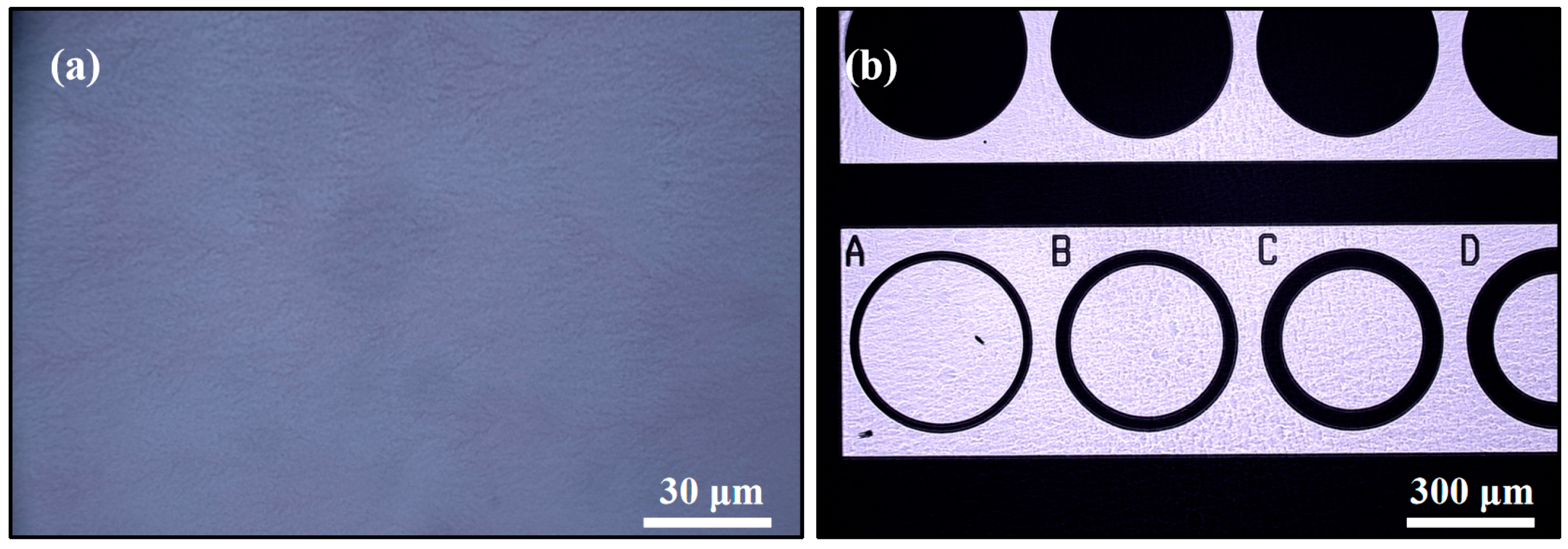
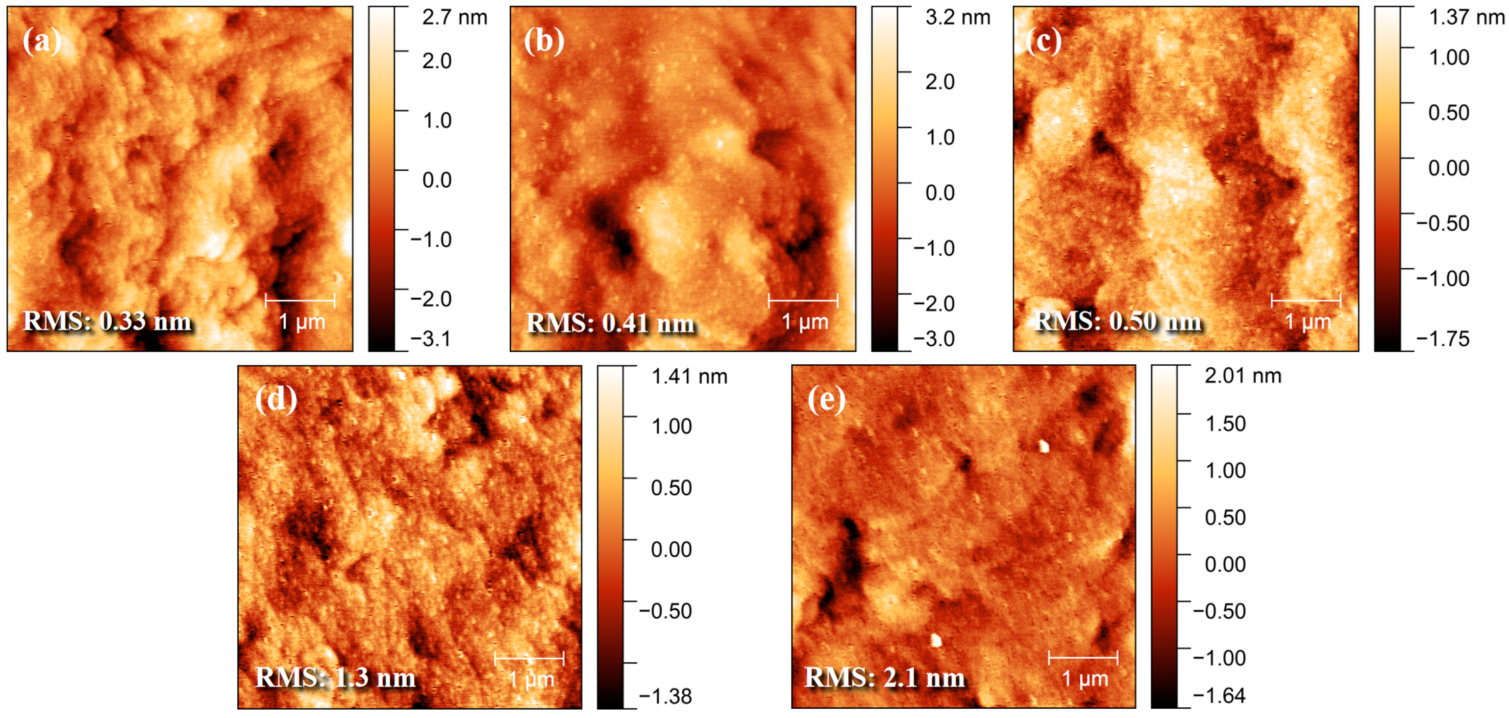
AFM was used to assess the effect of C doping on the surface morphology of the cGaN buffer. As shown in
Figure 4, the RMS roughness increases from 0.33 nm for A1 to 0.41 nm, 0.50 nm, 1.3 nm, and 2.1 nm for A2–A5, respectively. Only a slight increase in roughness is observed at low-to-moderate doping levels (A1–A3), indicating that the surface morphology is well maintained in this range. However, further increasing the C doping level to A4 and A5 results in a marked deterioration of the surface. This phenomenon, in which surface roughness increases monotonically with nominal doping concentration, is consistent with the results obtained from XRD testing. While the RMS roughness provides a general statistical measure of the surface, a closer inspection of the AFM topographical images (as shown in
Figure 4) reveals a more complex hierarchical relief. As correctly pointed out, the surface morphology is characterized by the coexistence of large-scale wavy features and small island-like structures. The large wavy features are typically associated with the step-bunching phenomenon, which occurs due to the step-flow growth mode and localized strain relaxation during the epitaxial process. Superimposed on these steps are densely distributed nanometer-scale small islands. These islands likely originate from localized 3D nucleation or the termination points of threading dislocations at the surface.
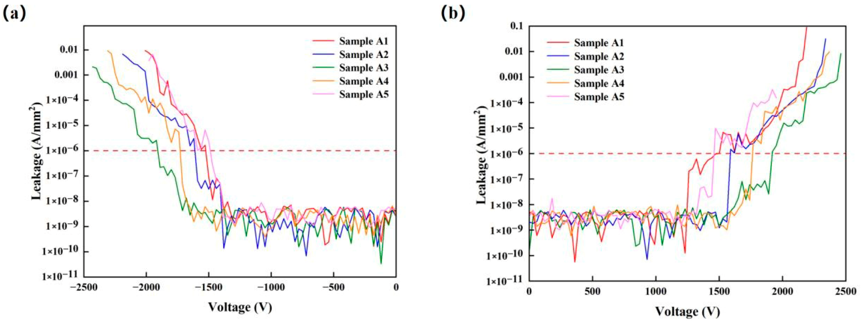
HV measurements were carried out to evaluate the effect of C doping on the lateral breakdown behavior of the cGaN buffer layer. As shown in
Figure 5, all samples exhibit very low leakage current (<10
−8 A/mm
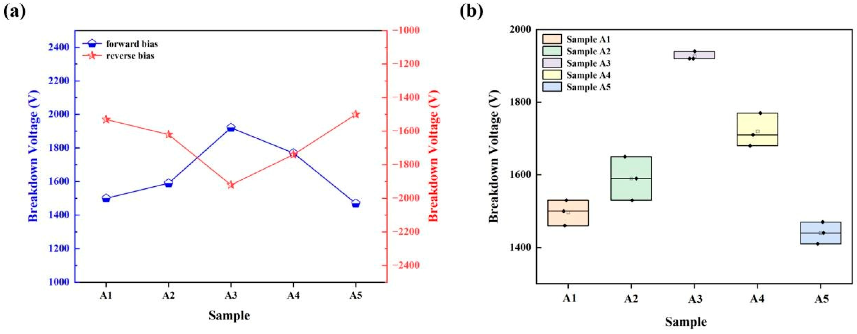
2) at low bias, followed by a sharp current increase at breakdown. Among them, A3 shows the best performance, maintaining low leakage current up to 1920 V and exhibiting symmetric breakdown characteristics with absolute breakdown voltages (|V
BR|) both of 1920 V for reverse and forward biases, respectively. In contrast, A1 and A5 break down at significantly lower voltages, indicating that either insufficient or excessive C doping is unfavorable for breakdown performance.
Figure 6b further confirms that A3 has the narrowest V
BR distribution, reflecting the best stability and reproducibility. The superior breakdown behavior of A3 arises from the synergistic optimization of compensation effect and crystal quality. In this work, V
BR was extracted using a current density of 1 × 10
−6 A/mm
2, which was chosen to limit excessive self-heating during high-voltage measurements and to allow consistent comparison with previous reports. It should be noted that the physical onset of hard breakdown, where the I-V characteristic sharply transitions from trap-mediated leakage to catastrophic breakdown, occurs slightly earlier.
Notably, the (002) and (102) reflection FWHM values of sample A3 (nominal C doping concentration of 4.69 × 1018 cm−3) are 394.3 and 566.7 arcsec, respectively, with TDDs of 9.81 × 108 cm−2. It shows moderately higher FWHM and dislocation density than the lightly doped samples A1 and A2, but outperforms the heavily doped A4 and A5. At the same time, the RMS of A3 is 0.50 nm, which is slightly higher than that of A1 and A2 but still significantly lower than those of A4 and A5. Moreover, the AFM images reveal a relatively uniform surface with clear grain boundaries and limited defects in A3, in contrast to the rough island-like and grooved morphologies observed in A4 and A5. This is in good agreement with the crystal quality results and provides further support for the superior electrical performance of A3. This unique positioning enables sample A3 to simultaneously benefit from moderate C doping while successfully avoiding the severe crystal quality degradation associated with excessive doping, thereby establishing a critical physical foundation for its superior breakdown performance.
The increase in breakdown voltage resulting from moderate C doping is consistent with the enhanced buffer compensation induced by C incorporation, through which vertical and lateral leakage pathways are effectively suppressed. At the same time, its relatively low TDDs and smooth surface help minimize defect-related trap states and electric-field inhomogeneity, delaying the onset of localized current percolation. In contrast, underdoping fails to sufficiently suppress background conduction, while overdoping degrades the crystal quality and surface morphology, leading to enhanced trap-assisted leakage, local field concentration, and earlier breakdown. As a result, the optimum carbon concentration is process-dependent and should be considered together with temperature, pressure, V/III ratio, and layer thickness. The nominal C concentration of A3 is the most favorable in this series under the present growth conditions, which achieved a trade-off between insulation capability and structural quality, giving rise to the highest and most stable lateral breakdown voltage.
3.2. The Effect of Buffer Thickness on Breakdown Characteristics of cGaN Buffer
To further optimize the cGaN buffer, the influence of buffer thickness on crystal quality was examined while keeping the nominal C concentration constant at 4.69 × 10
18 cm
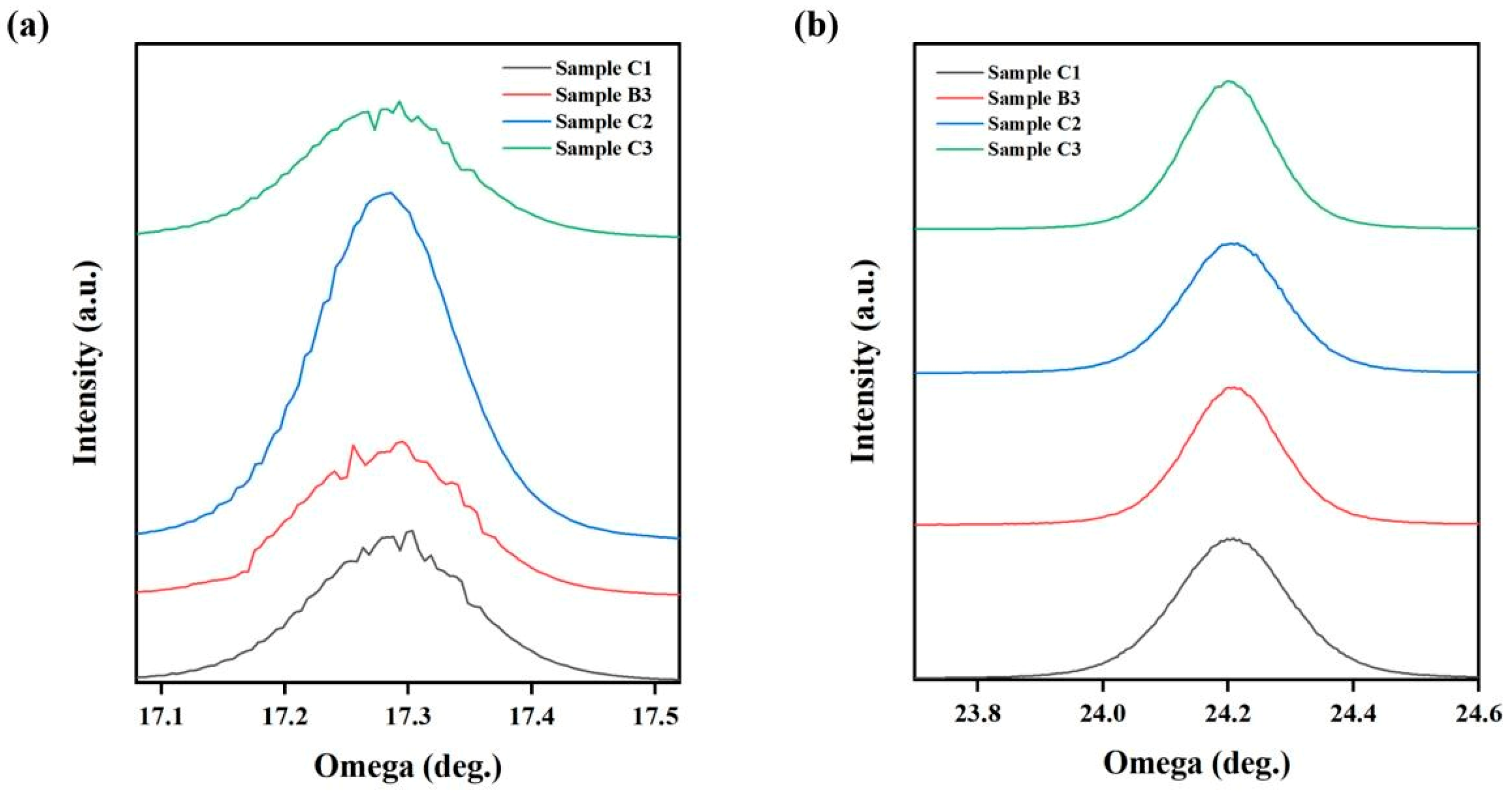
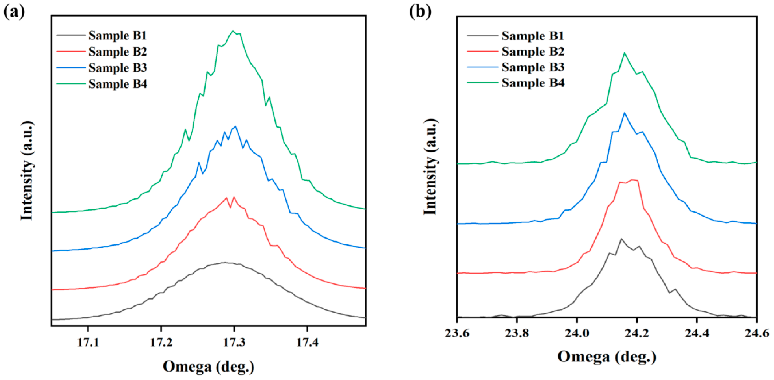
−3. HRXRD characterization was performed for samples B1–B4 with thicknesses ranging from 0.25 to 1.50 μm. As shown in
Figure 7 and
Table 3, the FWHMs of the (002) and (102) reflections first decrease and then increase with increasing thickness, revealing a non-monotonic thickness dependence of crystalline quality. Among all samples, B3 exhibits the narrowest diffraction linewidths, with minimum FWHMs of 449.6 arcsec for (002) and 582.3 arcsec for (102).
This evolution is consistent with the dislocation density analysis. For a relatively thin cGaN buffer such as B1 (TDDs ≈ 1.44 × 109 cm−2), the accommodation of lattice and thermal mismatch between GaN and sapphire may be insufficient, which can result in incomplete strain relaxation, less effective dislocation reduction, and degraded crystalline quality. Increasing the cGaN thickness can improve strain accommodation and defect reduction up to an optimized thickness under the growth conditions, thereby improving the crystal quality, which can be inferred from the reduction in FWHM and dislocation density. For example, B3 achieves the lowest TDDs of 1.07 × 109 cm−2.
In contrast, when the buffer thickness is further increased to 1.50 μm, the crystal quality deteriorates again. This may be related to changes in growth kinetics caused by an excessively thick buffer layer. Under optimized epitaxial conditions, GaN is expected to grow in an ideal 2D step-flow mode. However, during the prolonged epitaxy required for very thick layers, maintaining the strictly optimal growth window becomes challenging. The reduction in Ga adatom mobility disrupts the steady step-flow growth, promoting step bunching and macro-step formation, which manifests as the increased surface roughness observed in our samples. Furthermore, severe deviations can trigger a transition from 2D growth to 3D growth features, such as hillocks or microscopic faceting. Macroscopically, these morphological degradations induce severe structural instabilities, leading to the formation of new grain or tilt boundaries and the generation of secondary threading dislocations. This can also be verified by the subsequent AFM results.
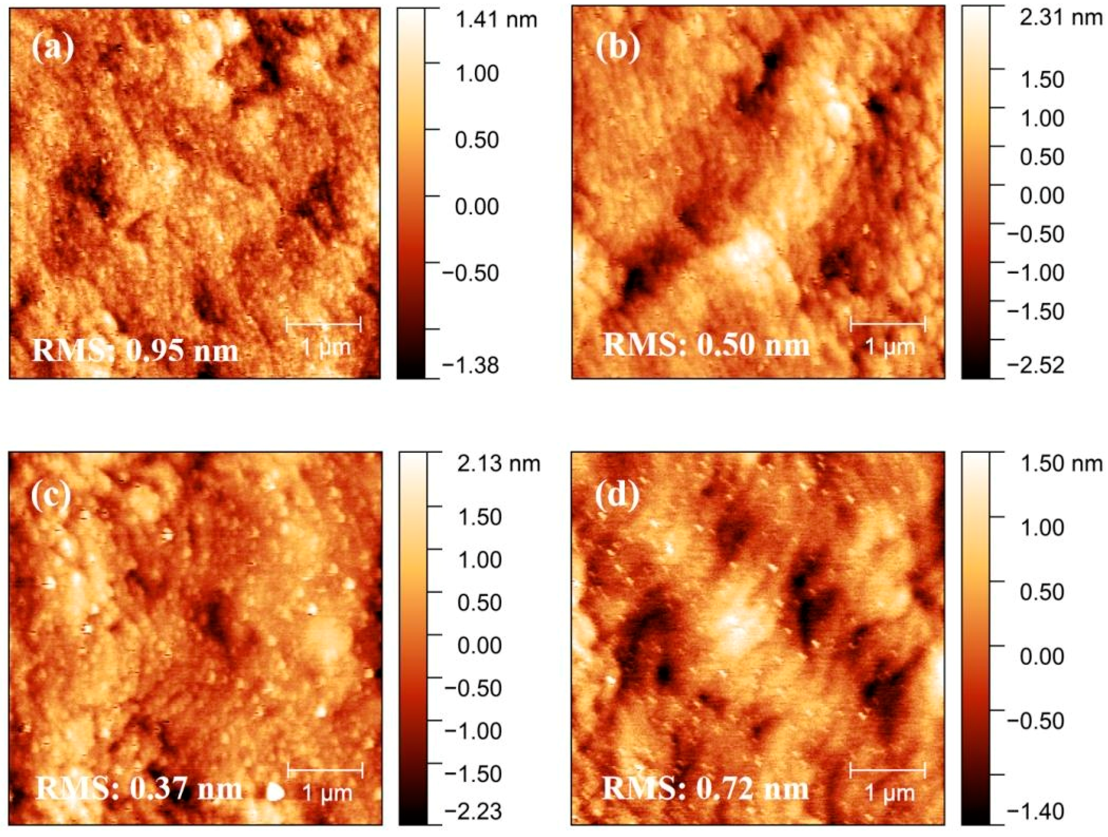
AFM characterization further corroborates the non-monotonic dependence of crystal quality on buffer thickness revealed by XRD. As shown in
Figure 8, the thinnest sample B1 shows pronounced surface undulations and island-like features (RMS ≈ 0.95 nm), consistent with its high dislocation density and broad diffraction peaks. As the buffer thickens to intermediate values (0.50 μm/1.00 μm), opportunities for dislocation interaction, bending, and annihilation increase, leading to markedly improved surface planarity. Sample B3 attains the lowest RMS (≈0.37 nm) and the minimum TDDs, showing that this thickness effectively balances strain relaxation with suppression of defect propagation. This indicates that an insufficient buffer thickness cannot adequately relieve lattice and thermal mismatch, allowing threading dislocations to reach the surface, impede adatom mobility, and disrupt step-flow growth, which together cause surface roughening.
Further increasing the buffer to 1.50 μm degrades both surface and crystal quality. This reversal can be attributed to accumulated strain energy and a prolonged growth/thermal history in thicker layers, which promote new defect formation, local stress concentration, and a transition toward more three-dimensional growth modes that suppress favorable step-flow kinetics. Therefore, the observed correspondence between AFM and XRD demonstrates that the surface instabilities may further generate structural imperfections, including grain or tilt boundaries and additional threading dislocations, which in turn deteriorate the electrical performance by increasing leakage pathways. Thus, the degradation at larger cGaN thicknesses is more reasonably attributed to non-optimal growth kinetics and morphology-induced defect formation, rather than to continued strain relaxation alone. It is worth noting that the non-monotonic dependence of dislocation density on buffer thickness may also be affected by the growth rate, which warrants further investigation in future work.
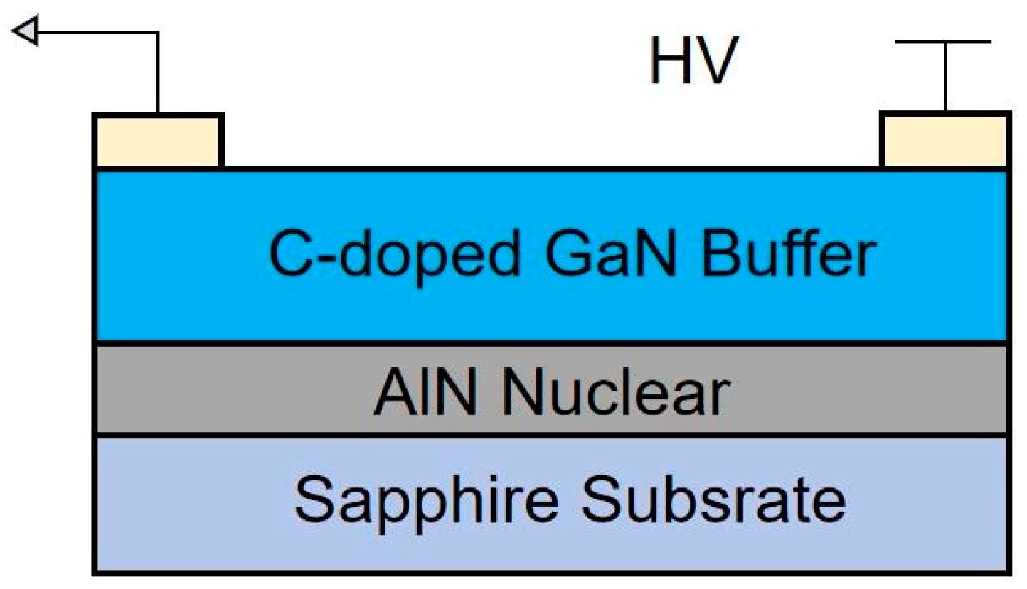
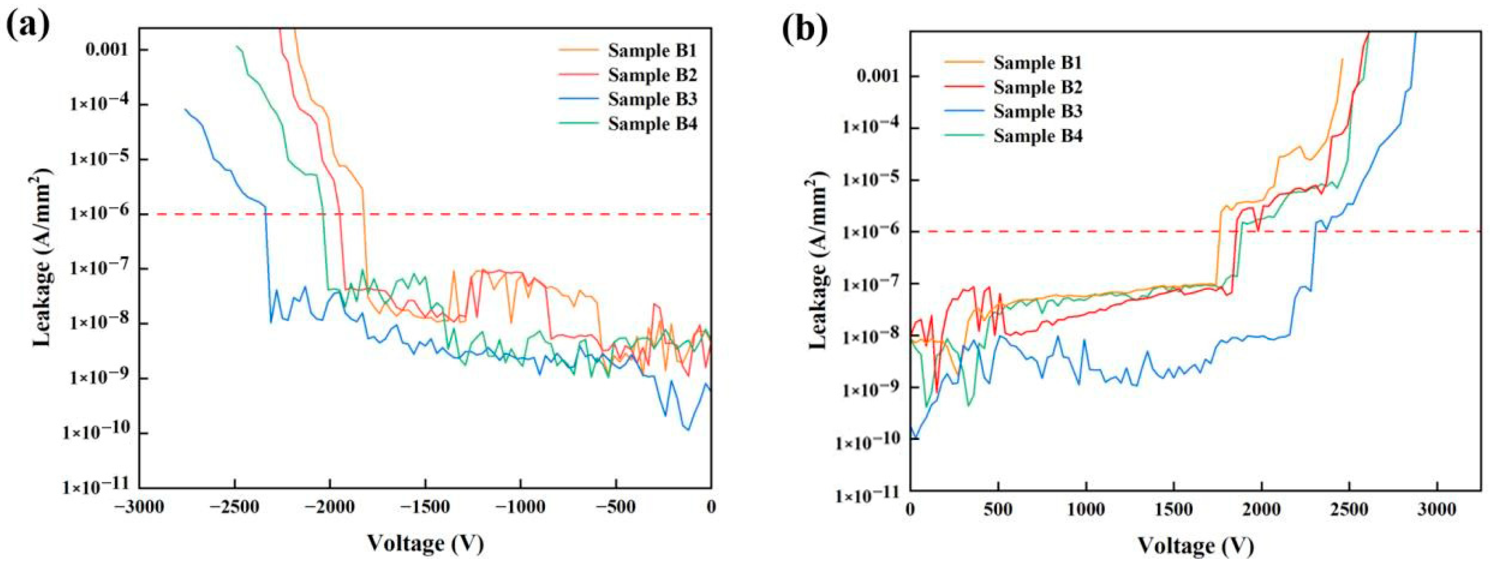
The lateral breakdown behavior was evaluated by HV measurements in a horizontal device geometry (
Figure 9a,b). Breakdown strongly depends on the cGaN buffer thickness. Under reverse bias, the thinnest sample in this series B1 (0.25 μm) with the highest TDDs (≈1.44 × 10
9 cm
−2) and roughest surface (RMS ≈ 0.95 nm) shows the poorest blocking (|V
BR| = 1830 V). Increasing the thickness to B2 (0.50 μm) yields a modest improvement (|V
BR| = 1950 V) associated with reduced TDDs and smoother surface. The best reverse performance occurs at B3 (1.00 μm), which reaches 2340 V and coincides with the lowest TDDs (≈1.07 × 10
9 cm
−2) and minimal RMS (0.37 nm). Further thickening to B4 (1.50 μm) degrades the blocking ability (|V
BR| = 2040 V) as TDDs and surface roughness rise again. The forward bias trends mirror the reverse case: B3 yields the highest forward breakdown (|V
BR| = 2310 V), while both thin and over-thick buffers show reduced forward blocking (|V
BR| = 1770 V for B1; |V
BR| = 1880 V for B4). This bilateral behavior implies that buffer quality—not bias polarity—controls lateral breakdown.
Mechanistically, the thickness dependence reflects a trade-off between strain relaxation and defect generation. An insufficient buffer thickness allows threading dislocations to propagate to the surface, creating leakage paths and local field-enhancement sites that trigger premature impact ionization and breakdown. Moderate thickness (around 1.00 μm) promotes dislocation bending, interaction and partial annihilation during growth, yielding fewer conductive defect channels, more uniform field distribution, and improved surface planarity—together delaying avalanche onset. Excessive thickness, however, accumulates strain energy and extends the growth/thermal history, which can nucleate new defects, enhance local stress concentrations, and induce more three-dimensional growth modes; these effects revive defect-assisted leakage and lower the effective blocking voltage.
In summary, the lateral breakdown voltage exhibits a pronounced non-monotonic dependence on the cGaN buffer thickness. Under our present growth window, the highest and most symmetric breakdown performance is achieved at approximately 1.00 μm, a point where defect annihilation is maximized before the onset of growth kinetic degradation. Rather than indicating an absolute thickness limit, the deterioration in thicker layers emphasizes the necessity of maintaining stable step-flow growth kinetics during prolonged epitaxy. More importantly, realizing high-voltage cGaN buffer layers requires coupling these stabilized growth conditions with a meticulously optimized nominal carbon concentration window. While sufficient carbon incorporation is crucial to compensate background shallow donors and increase the buffer resistivity, excessive carbon doping must be avoided to prevent introducing additional defect-related penalties that would otherwise compromise the device performance.
3.3. The Effect of AlN Nucleation Layer Thickness on Breakdown Characteristics of the cGaN Buffer
The AlN nucleation layer thickness strongly controls cGaN crystal quality via dislocation filtering and strain management mechanisms. Four samples with AlN thicknesses of 320 nm, 400 nm, 480 nm and 640 nm were compared by HRXRD (
Figure 10) and the best crystal quality was obtained near 480 nm as shown in
Table 4. A too thin AlN layer seemingly cannot sufficiently accommodate lattice mismatch or induce the bending/trapping of threading dislocations at the substrate–buffer interface, so defects readily propagate into the GaN (highest TDDs observed for 320 nm). Moderately thick AlN (around 400 nm) already enhances elastic strain relief and promotes dislocation interaction and annihilation, improving FWHM and reducing TDDs. Extending thickness to 480 nm further approaches the ideal balance: the nucleation layer provides enough thickness to redistribute mismatch stress and generate favorable glide/bending of dislocations without introducing new intrinsic defects or interface roughness, yielding the minimum measured TDDs. Beyond this practical thickness range (e.g., above 640 nm in our samples), increased AlN thickness tends to correlate with increased defect generation and surface roughening. This may be attributed to a combination of factors, potentially including accumulated tensile stress within the AlN layer and a transition towards less ideal, more three-dimensional overgrowth modes, which can reintroduce stress concentrations and facilitate new defect nucleation, thus diminishing the structural and electrical benefits.
In short, within the investigated range, the AlN nucleation layer shows a non-monotonic influence on crystal quality. The intermediate thickness of 480 nm gives the lowest XRD rocking-curve FWHM and the smoothest AFM surface among the samples studied, indicating improved crystalline quality and reduced surface roughness. Both thinner and thicker AlN layers lead to inferior results. Combining the optimized AlN layer with the previously identified cGaN buffer (1.00 μm) and nominal C doping concentration yields the best overall structural performance in this sample set.
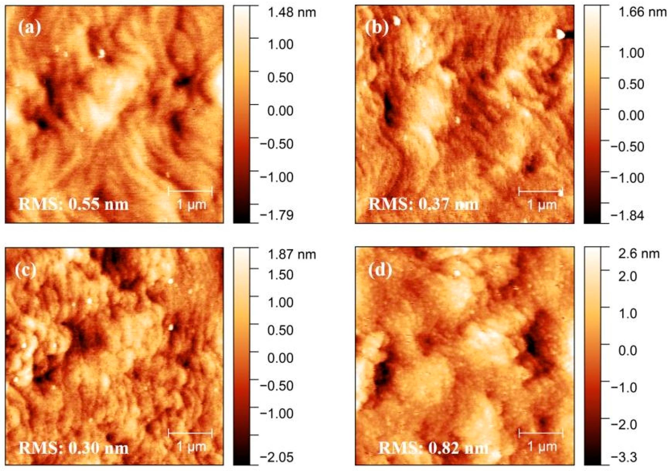
AFM results, as shown in
Figure 11, indicate that the cGaN layer surface morphology depends on the AlN nucleation layer thickness within the present growth window. For the thinner AlN layer (320 nm), the surface morphology is comparatively rough, which is consistent with insufficient accommodation of lattice and thermal mismatch near the AlN/GaN interface. In this case, threading dislocations may propagate more readily into the GaN layer, leading to dislocation-related growth perturbations such as hillock formation and irregular terraces, as reflected by the higher roughness (RMS ≈ 0.55 nm). By contrast, when the AlN thickness increases to an intermediate range (e.g., 400~480 nm), the surface becomes noticeably smoother. The 480 nm sample, in particular, shows the clearest atomic terraces and the lowest roughness (RMS ≈ 0.30 nm). This trend suggests that the intermediate AlN thickness provides a more favorable growth template, which may help suppress dislocation-related surface disturbances and promote a more uniform step-flow-like growth mode.
However, further increasing the AlN thickness to 640 nm degrades the morphology again (RMS ≈ 0.82 nm), indicating that the benefit of a thicker nucleation layer is not unlimited. Once the AlN layer becomes excessively thick, accumulated internal stress within the AlN layer itself may no longer be efficiently accommodated and may instead influence the GaN overlayer in a less uniform manner. At the same time, an overly thick AlN template may be more susceptible to additional structural imperfections or interfacial roughness, which would weaken its role as an ideal epitaxial template. These effects may destabilize step-flow growth and promote local three-dimensional nucleation or mound formation during the early GaN growth stage, leading to renewed roughening.
Overall, an intermediate thickness near 480 nm provides the most favorable balance within the present growth window: it is thick enough to improve the surface roughness and the step-flow growth pattern of the material and suppress the vertical propagation of threading dislocations, but not so thick that the AlN layer itself appears to introduce additional stress concentration or structural degradation. This interpretation is consistent with the observation that the smoothest surface is obtained only within a limited thickness window rather than by continuously increasing the AlN thickness.
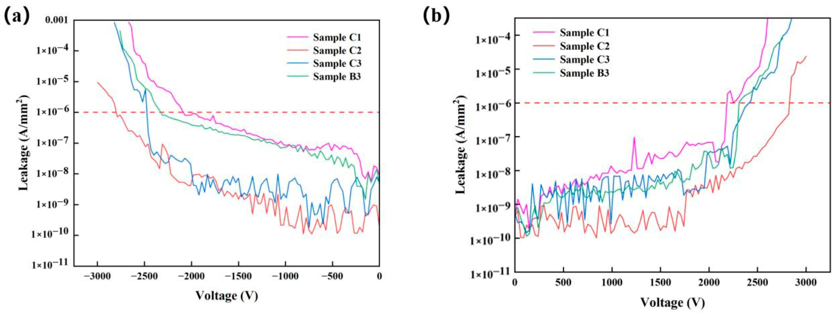
Lateral electrical testing shows a clear correlation between AlN nucleation thickness, buffer quality, and high-voltage performance in
Figure 12. The best lateral breakdown is observed for sample C2 (AlN = 480 nm), with symmetric forward and reverse |V
BR| of 2850 V and the lowest mid-to-high voltage leakage (10
−9~10
−8 A/mm
2). Considering the 30 μm gap distance, this translates to a lateral E
BR of approximately 0.95 MV/cm. This behavior is consistent with the improved structural quality of this sample, including the reduced threading dislocation density and the smoother surface morphology. A lower density of extended defects and a flatter surface are both expected to reduce local current leakage pathways and mitigate field enhancement at morphological irregularities. In addition, a more structurally uniform buffer may support a more homogeneous internal field distribution, which can help delay electrical failure under high bias. Together, these factors are consistent with the enhanced breakdown performance and reduced leakage observed for the intermediate-thickness sample.
By contrast, both the thin sample C1 (AlN = 320 nm) and the overly thick sample C3 (AlN = 640 nm) show reduced |VBR| and higher leakage. For the thin case, insufficient strain accommodation may leave more threading dislocations unfiltered, and the associated defects may contribute to local leakage conduction and earlier electrical failure. For the excessively thick case, accumulated internal stress, degraded AlN layer quality, and possible interfacial roughness may introduce additional localized high-field regions and defect-related leakage paths, which can weaken the lateral blocking capability. The intermediate sample B3 (AlN = 400 nm) shows intermediate electrical performance, consistent with a gradual improvement in buffer quality as thickness approaches the favorable range.
The close forward/reverse symmetry of |VBR| across samples indicates that breakdown is likely governed by the overall buffer quality and field distribution rather than by a strong polarity-dependent interface effect. Small forward/reverse differences in individual devices likely reflect local microstructural variation or electrode-edge field effects rather than a systematic polarity dependence. In summary, AlN thickness tuning within the present growth window has a strong influence on electrically active defects, surface morphology, and field distribution, thereby affecting lateral blocking capability; deviations on either side of the favorable thickness range are associated with increased leakage and lower |VBR|.
3.4. Preliminary Investigation of Low Pressure and Reduced V/III Treatments on Breakdown Characteristics of the Buffer Performance
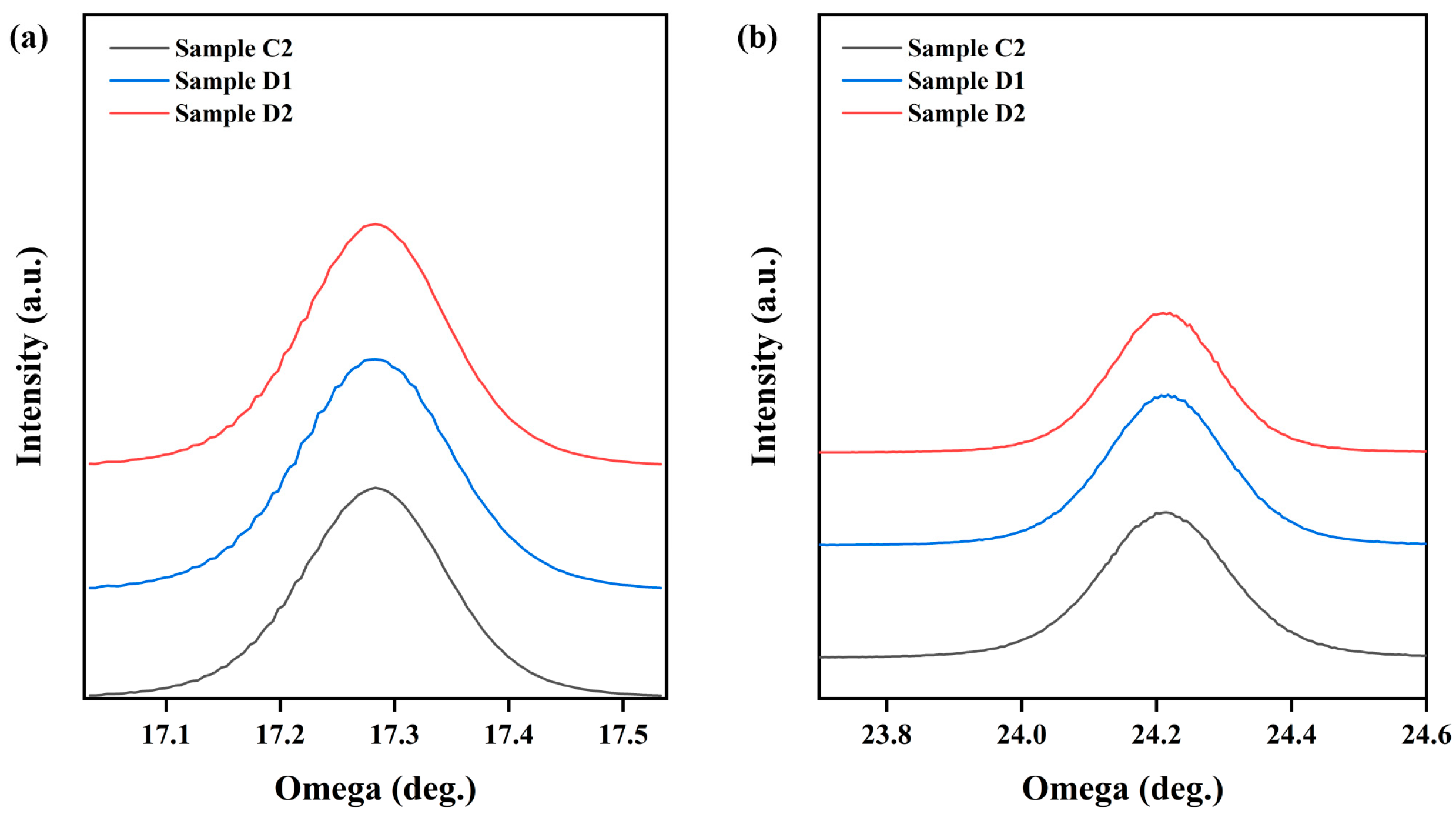
Building on the optimized baseline C2, we further investigated the influence of growth pressure and V/III ratio on the crystalline quality and breakdown characteristics of cGaN. By reducing the growth pressure from 300 to 50 mbar (sample D1) and subsequently lowering the NH
3 flow rate (sample D2), a progressive narrowing of HRXRD (002) and (102) rocking curves was observed as shown in
Figure 13, corresponding to a monotonic decrease in TDDs from 1.03 × 10
9 cm
−2 in C2 to 8.38 × 10
8 cm
−2 in D2 (
Table 5).
The observed improvements arise from the synergistic modification of surface kinetics and precursor chemistry. Lowering the reactor pressure increases the mean free path of Ga adatoms, which effectively extends their diffusion length. This promotes a 2D step-flow growth mode, suppressing 3D island nucleation—a primary source of threading dislocations—and facilitating the lateral annihilation of existing dislocations. Concurrently, a reduced V/III ratio minimizes kinetic constraints by decreasing surface competition from excess nitrogen species and suppressing parasitic gas-phase prereactions. The resulting increase in Ga adatom residence time further enhances lateral incorporation at step edges. These mechanisms—pressure-driven diffusion enhancement and V/III ratio-driven barrier reduction—collectively bias the growth process toward defect-reducing surface kinetics. These results demonstrate that when implemented on a well-engineered heterointerface, sequential optimization of these growth parameters provides a scalable pathway for defect suppression in cGaN epitaxy.
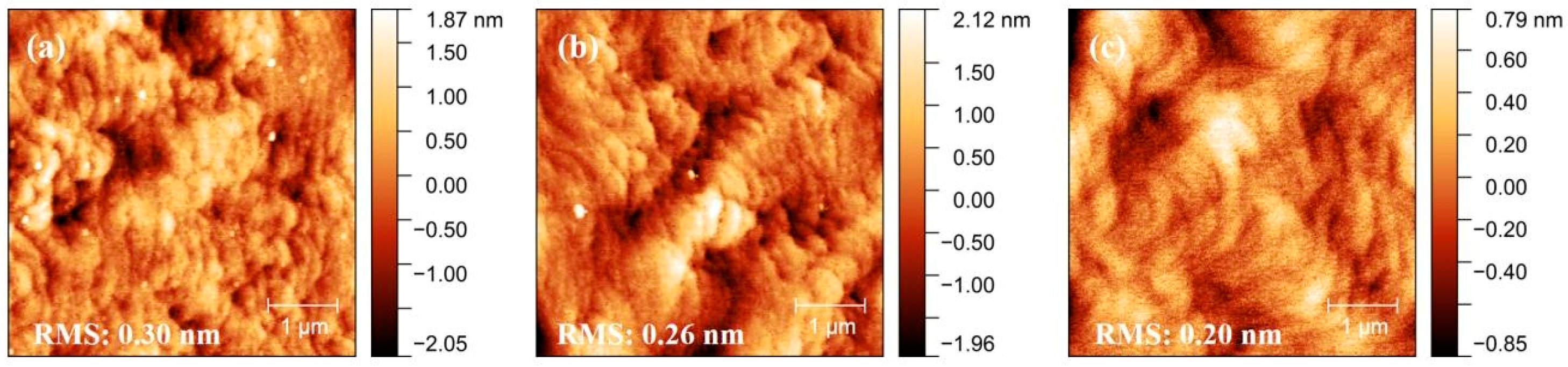
AFM characterization reveals progressive surface refinement across the optimization series as shown in
Figure 14. Sample C2 exhibits RMS roughness of 0.30 nm with characteristic undulating morphology. Sample D1, grown at reduced pressure (50 mbar), shows improved surface flatness with RMS roughness of 0.26 nm, reflecting enhanced step-flow growth kinetics from increased Ga adatom surface diffusion. Lower pressure reduces interstep distances and promotes uniform lateral growth, minimizing 3D island formation.
Sample D2, with additionally reduced NH3 flow rate, achieves the lowest RMS roughness of 0.20 nm, demonstrating the cumulative benefit of dual optimization. The superior surface flatness originates from synergistic interplay between low-pressure enhancement of Ga adatom migration and reduced V/III ratio alleviation of kinetic constraints on lateral diffusion, both promoting optimal 2D step-flow growth. Mechanistically, diminished NH3 flow suppresses parasitic side reactions and reduces surface contamination, enabling cleaner, more ordered growth surfaces. Additionally, lower V/III ratio reduces nitrogen-induced adsorption competition, prolonging Ga residence time and facilitating step-edge incorporation that favors smooth terrace formation over island nucleation.
The surface morphology progression directly correlates with XRD-derived defect densities: smoother surfaces reflect superior crystalline ordering, as reduced roughness minimizes nucleation sites for defect formation during growth. The inverse relationship between surface roughness and dislocation density confirms that step-flow growth geometry—enabled by optimized surface kinetics—suppresses dislocation generation and propagation. Collectively, decreasing FWHM, TDDs and surface roughness demonstrate that sequential parameter optimization synergistically enhances cGaN buffer structural quality through complementary mechanisms governing surface diffusion kinetics and growth mode selection. But practical limits remain: overly low pressure or V/III can upset stoichiometry or introduce other defects, so the observed improvements pertain to the explored parameter window.
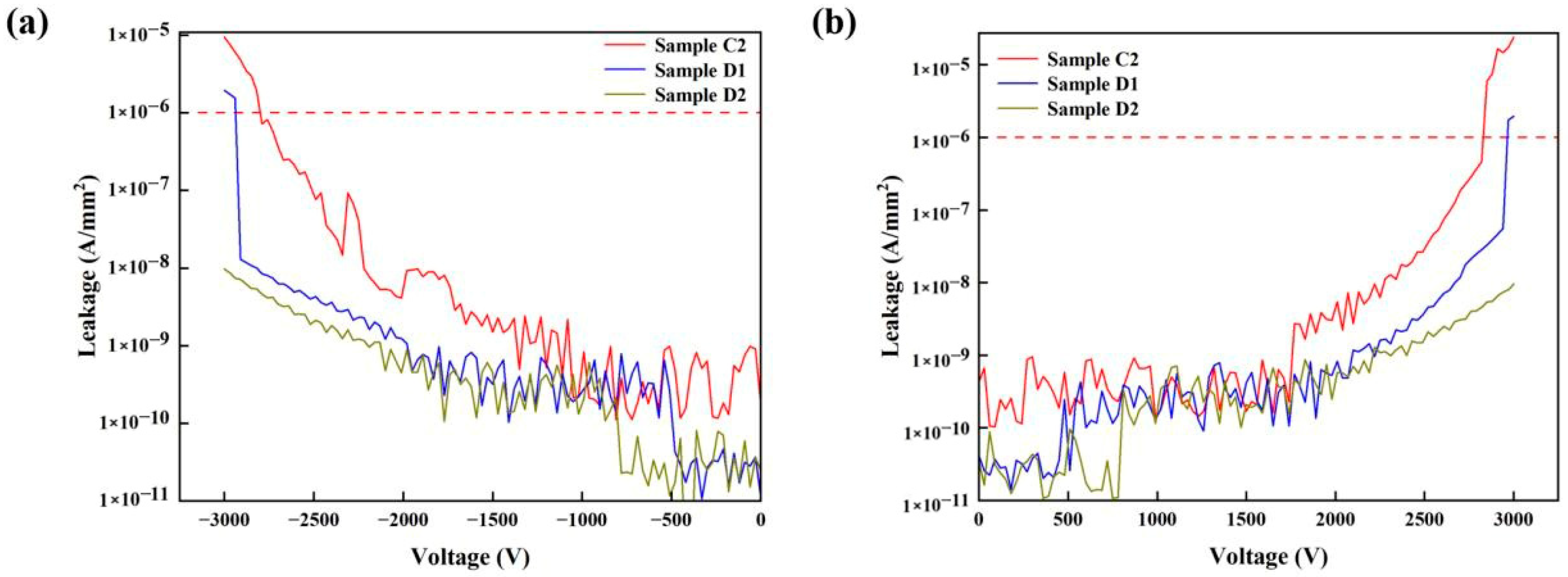
Electrical characterization of samples reveals progressive performance enhancement correlating with structural quality improvements as shown in
Figure 15. Sample C2 exhibits |V
BR| of 2850 V for reverse bias with elevated reverse leakage current (~1 × 10
−8 A/mm
2 at high bias), attributable to its higher TDDs (1.03 × 10
9 cm
−2) and rougher surface (RMS ≈ 0.30 nm).
Sample D1, incorporating reduced-pressure growth, shows marginal improvement: |VBR| of 2940 V (+3.2% vs. C2) with reduced reverse leakage current correlated with lower TDDs (9.35 × 108 cm−2) and improved surface (RMS ≈ 0.26 nm). This modest enhancement reflects the limited effectiveness of structural optimization alone in suppressing defect-mediated conduction. Sample D2, with combined reduced pressure and reduced NH3 flow, exhibits exceptional performance: no measurable breakdown within the testing limit and leakage current suppressed 1~2 orders of magnitude below C2 and D1 across the entire voltage range. The measured breakdown voltage of >3000 V corresponds to a breakdown electric field of approximately >1.0 MV/cm for the given electrode spacing of 30 μm.
Forward bias characteristics (
Figure 15b) corroborate these findings: C2 exhibits 2850 V forward breakdown with steeply rising forward leakage, D1 shows 2970 V (+4.2%) with improved suppression and D2 shows no breakdown within the measurement window with dramatically suppressed forward leakage, reflecting symmetric behavior consistent with bulk-limited conduction in a semi-insulating material.
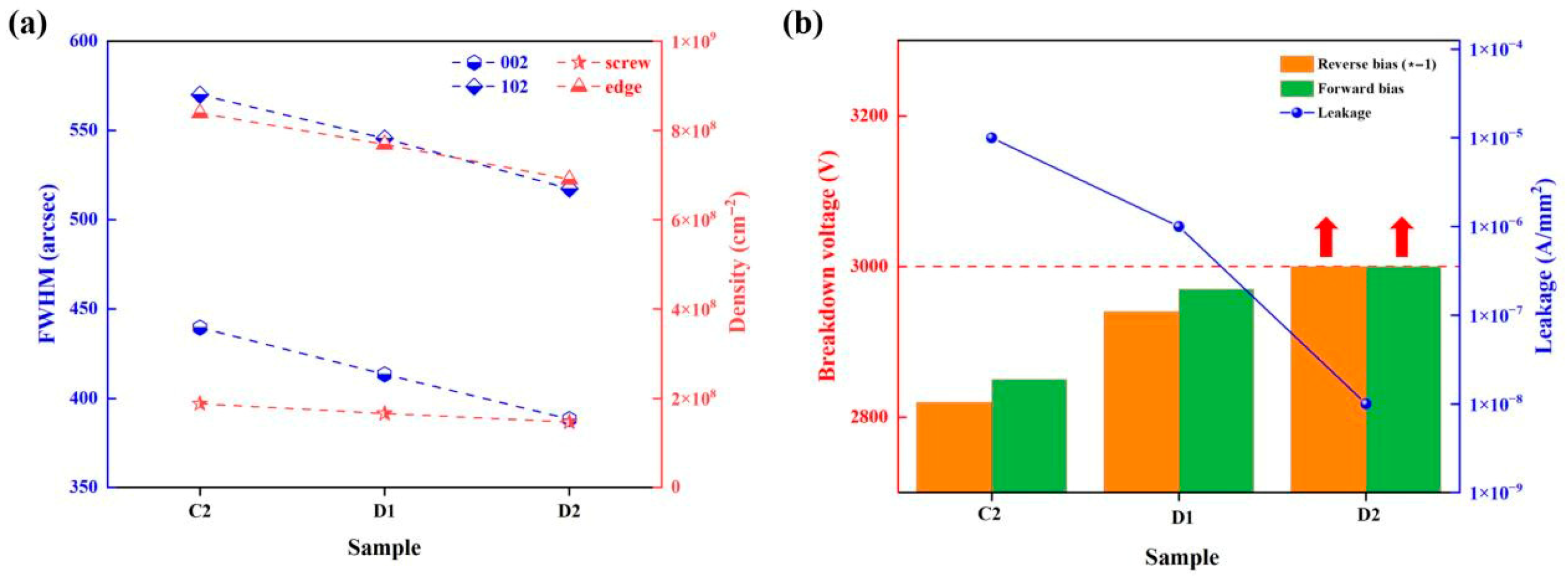
The progression from C2 to D1 demonstrates that pressure reduction alone yields consistent but modest improvement through enhanced surface diffusion and reduced dislocations (
Figure 16a). However, the extraordinary leap from D1 to D2 as shown in
Figure 16b—manifested in breakdown suppression and 1~2-order-of-magnitude leakage reduction—may be related to the combined effect of improved structural quality and modified compensation conditions under the reduced V/III ratio. Based on our previous SIMS calibration for the GaN growth window, a reduced V/III ratio may favor stronger carbon incorporation under similar growth conditions, which could in turn modify the compensation state and influence the leakage behavior. At the same time, practical caveats are also important that excessive carbon or too low V/III can introduce deep compensating states distributed unfavorably or produce stoichiometric imbalance and new defect species; similarly, extreme pressure reduction may destabilize growth uniformity. Thus the pronounced enhancement observed for D2 pertains to the optimized window explored here, where kinetic and compositional tuning are relatively balanced to minimize active defects and maximize bulk resistivity.