1. Introduction
Optical thin films are vital components in modern optical systems [
1], and the quality of their manufacturing significantly affects overall system performance. However, various factors during the manufacturing process, such as the precision of the coating equipment, the properties of the coating materials, and the conditions under which the process takes place, can lead to microscopic defects like particles, spots, and scratches on the films. These defects can severely compromise the functionality and performance of optical thin films. Typically, traditional manual inspection methods depend on human operators to identify and eliminate defective samples, but these approaches are often inefficient and prone to high error rates [
2]. With the rapid advancement of deep learning technology [
3,
4], there is growing interest in applying it to the automated detection of microscopic defects in optical thin films. While deep learning has demonstrated significant success in various domains, the unique challenges associated with detecting microdefects in optical thin films remain substantial.
Surface defect detection has been widely studied in various domains, including metal surfaces, semiconductor wafers, and glass substrates. Traditional computer vision methods, including edge detection, thresholding, and morphological operations, have demonstrated some success but are often sensitive to noise and variations in lighting conditions. With the rise of artificial intelligence (AI), convolutional neural networks (CNNs) provide algorithms that enable machines to effectively identify patterns, objects, and features in visual data [
5]. CNNs are the key technology behind computer vision. CNNs are a class of machine learning algorithms that have been applied to image classification [
6], feature detection [
7], image segmentation [
8], and object recognition problems [
9]. CNNs have achieved classification accuracy comparable to that of human experts in computer vision challenges [
10,
11]. The performance and robustness demonstrated by CNNs make them attractive for analyzing thin-film defects. Another advantage of CNNs is that they can be easily trained using samples provided by domain experts (such as materials scientists), eliminating the need for complex algorithmic customization by computer vision experts [
12]. CNNs are a well-established method for analyzing electron microscopy images. Examples of their application in materials science include mechanical property estimation [
13], nanoparticle segmentation [
14], nanostructure classification [
15], and atomic-scale defect investigation [
16,
17,
18].
In recent years, the introduction of artificial intelligence into automated optical inspection (AOI) systems has attracted widespread attention [
19]. AI-based AOI systems have been widely applied across various fields, substantially improving the inspection processes in production lines. Jian et al. [
20] proposed an automatic surface defect detection method based on machine vision for mobile phone screen glass. The method integrates image processing, region enhancement, and convolutional neural networks, achieving favorable detection performance in experimental settings. Similarly, Kuo et al. [
21] developed an automated inspection approach for polarizer film defects by integrating image processing and classification techniques. Using filtering, image segmentation, and morphological operations to extract defect features, and combining these with deep learning models, their system achieved a classification accuracy of 98.9%. Chen et al. [
22] introduced an automatic crack segmentation method utilizing deep learning-based high-resolution representation learning. The approach extracts deep features from high-resolution images to perform precise crack segmentation. Tests on multiple public datasets demonstrated the method’s significant improvement in segmentation performance. Zhao et al. [
23] presented a real-time full-surface defect recognition system for soybean seeds based on deep learning. The system can efficiently classify large datasets by employing a novel convolutional neural network model. Incorporating image preprocessing and data augmentation techniques further enhanced system accuracy, achieving a recognition rate of 94%. Lim et al. [
24] proposed a PCB defect detection model based on deep contextual learning and successfully implemented an anomaly trend alert system. This method extracts deep features from PCB images and integrates contextual information into the feature extraction process for accurate defect detection.
For the microscopic defect detection, Karangwa et al. [
25] proposed an automated optical inspection platform for real-time detection of surface defects on planar optical components based on semantic segmentation. By leveraging image processing and deep learning techniques, the system successfully identified defects such as scratches and fingerprints. Similarly, Zheng et al. [
26] developed a real-time batch inspection system for surface defects on circular optical filters. The system utilizes machine vision technology to detect various types of surface defects, including blemishes, scratches, and stains, with a final model accuracy of 98.3%. With the rise of deep learning, CNN-based architectures such as Faster R-CNN, SSD, and YOLO (You Only Look Once) have emerged as powerful tools for object detection [
27]. Among them, the YOLO family of models is known for its balance between speed and accuracy. Yang et al. [
28] proposed a deep learning-based method for detecting subtle surface defects on visual optical lenses, specifically targeting issues such as spots and delamination. The method was evaluated against YOLOv5 and YOLOv7 models, showing significant improvements in average precision, F1 score, and recall compared to YOLOv5, and further enhancements in both accuracy and speed compared to YOLOv7, demonstrating the effectiveness and efficiency of the proposed approach. Liang et al. [
29] introduced a surface defect detection method for optical components based on multi-scale hybrid kernels and structural re-parameterization. By incorporating five different multi-scale hybrid kernels into a deep learning model, their approach achieved a high accuracy of 97.39% to identify defects such as scratches and bubbles. Yang et al. [
30] proposed a scalable framework for thin-film defect detection based on computer vision, utilizing imbalanced regression and classification techniques. The method integrates deep learning, an attention mechanism, and an embedded system to identify eight defect types, including scratches and cracks, effectively. Furthermore, Liang et al. [
31] developed a weak scratch detection method for optical surfaces using a multimodal imaging system in conjunction with a deep encoder–decoder network. This system can produce more explicit images and is combined with a deep learning algorithm to segment surface scratches effectively. In 2024, Chen et al. [
32] proposed a real-time detection method named AMS-YOLO base on lightweight deep convolutional neural network for MicroLED defects with low distinction. AMS-YOLO outperformed the single-stage models SSD and RetinaNet in terms of accuracy and speed, with FPS faster by 84.8% and 93.6%, respectively. In 2025, Li et al. [
33] proposed an improved YOLOv8 detection algorithm that meets the accuracy and real-time speed requirements for defect detection in steel strip production. Their experimental results indicate that the improved model achieves a mean average precision (mAP) of 79.0%, compared to 65.8% for the original model, marking an improvement of 13.2%. In the same year, Su et al. [
34] reported a novel methodology for intelligent defect detection in additive manufacturing (AM) components with reflective surfaces, leveraging virtual polarization filtering (IEVPF) and an improved YOLO V5-W model. Their experimental results show a 40.3% reduction in loss, a 10.8% improvement in precision, a 10.3% improvement in recall, and a 13.7% improvement in mAP compared to the original YOLO V5 model.
The recent YOLOv7 architecture introduces architectural optimizations, including extended efficient layer aggregation networks (ELANs) and model re-parameterization techniques, which make it suitable for real-time detection tasks without sacrificing accuracy. While deep learning has been applied to detect defects in textiles and printed circuit boards (PCBs), fewer studies focus on microscopic thin-film coatings. Our work addresses this gap by tailoring a YOLOv7-based detection pipeline for the unique challenges of micro-scale surface defect imaging. Recent advancements in deep learning, particularly convolutional neural networks (CNNs), have significantly improved object detection and classification tasks. These developments offer promising avenues for automated surface defect detection in thin-film coatings, especially when combined with high-resolution optical microscopy.
The core innovation of this research is the application of the deep learning YOLOv7 model framework to solve the problem of detecting microscopic defects in optical thin films. This study presents a novel approach for detecting and classifying microscopic defects on the surface of optical thin-film coatings using deep learning, specifically the YOLOv7 object detection framework. By incorporating image augmentation, expert annotations, and fine-tuned model optimization, we developed a robust defect detection system capable of identifying and classifying four common types of thin-film coating defects: particles, speckles, scratches, and cracks. To achieve this, we designed a deep learning algorithm to enhance the accuracy and efficiency of defect detection, significantly reducing the time and cost of manual inspection while improving coating quality. By overcoming the limitations of traditional inspection techniques, our proposed microscopic thin-film defect detection system provides a more sensitive, reliable, and efficient solution, supporting the development of advanced optical coating technologies. The contributions of this paper include: (1) a microscopy-sensing data pipeline and expert annotation protocol for four types of thin-film defects; (2) a YOLOv7-specific training strategy for optimizing low-contrast and sub-pixel feature detection (focusing on enhancement and multi-scale tiling of microscopic objects); and (3) practical evaluation and deployment recommendations including confusion matrix, category-level AP, and F1 curves. These results demonstrate a balanced and feasible method for detecting microscopic thin-film defects.
2. Methods
2.1. Thin-Film Preparation
Thin films were prepared using an electron gun evaporation system associated with an ion-assisted deposition technique. The coating equipment is described as follows: The vacuum system consists of an oil rotary pump, a mechanical booster pump for rough evacuation, a diffusion pump for fine evacuation, and a helium cold trap to capture water vapor in the form of helium condensation in an air compressor to help improve the efficiency of the evacuation rate. The background pressure was 2.5 × 10⁻⁴ Pa. The working gases used are argon (99.999%) and oxygen (99.999%). The maximum output power of the electron gun is 10 kW, the voltage is 10 kV, and the current is 1 A. Ion-assisted deposition is primarily used to enhance adhesion on metal oxides. The Cu, WO3, Nb2O5 and SiO2 coating materials were supplied from Yimei Company (Taoyuan, Taiwan). B270 glass and silicon wafer have been used as substrates. The coating substrates have been preconditioned by plasma etching, and no adhesion layers have been deposited. The evaporation materials used in the process are all grain-like, with a particle size of about 2–5 mm and a purity of 99.99%. The evaporation geometry was optimized with respect to the specific demands of metal coating, so the distance from evaporation surface to the substrate was only 80 cm. Before thin-film deposition, evaporated materials will be pre-melted with an electron beam with a power of 2.0 kW. The material was evaporated by an electron beam with a power of 3.0 kW. The coating substrates were heated to 150 °C during the process. The anode current of the ion source for ion-assisted deposition is 0.5–10 A, the anode voltage is 80–300 V, the ion energy is 50–200 eV, and the divergence angle is 60 degrees. In this study, the deposition of Cu, WO3, Nb2O5, and SiO2 thin films using an electron gun evaporation system combined with ion-assisted deposition (IAD) required a series of tightly controlled processes to ensure the desired film properties. The vacuum value during the thin-film deposition process is approximately 5.7–6.5 × 10⁻⁴ Pa. The Cu and SiO2 thin films were deposited at a rate of 4 Å/s, while the WO3 and Nb2O5 thin films were deposited at a rate of 0.8–1.0 Å/s. The thicknesses have been controlled by quartz crystal monitoring. The quartz monitoring system uses a 5 MHz quartz crystal oscillator.
2.2. Microscopic Defect Generated by Thin-Film Coatings
The images of thin-film microdefects are all from various coating samples collected by our team. The causes of thin-film microdefects in high-vacuum electron-beam evaporation are complex. This article briefly introduces four possible causes of coating microdefects, including particles, speckles, scratches, and cracks. The causes and formation mechanisms of these four defect types are analyzed below.
- (1)
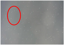
Particles: These particles appear as discrete nodules or raised spots on the film surface and typically originate from the “spraying” of large particles during electron beam evaporation. Localized overheating or rapid boiling of the melt source can cause droplets or solid fragments to be ejected and land on the substrate. Other sources include flaking of oxide crusts from the melt, crucible erosion, or loose contaminants in the chamber. These particles become embedded in the growing film, causing light scattering, surface roughening, and localized delamination.
- (2)
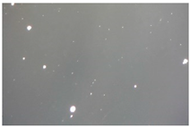
Speckles: Speckle-like microdefects appear as small circular or irregular contrast regions on the coating surface. They often arise from microdroplets, localized oxidation, or contamination by residual gases such as O2 or Ar during the deposition process. Transient arc events or micro-explosions in the e-beam source can also produce tiny pits or hillocks. Additionally, incomplete nucleation or island coalescence during early film growth can result in uneven microstructures, which manifest as optical speckles.
- (3)
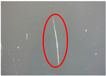
Scratches: Linear defects or grooves on the film typically result from mechanical damage before or after deposition. During the coating process, insufficient substrate hardness or particle embedding, followed by dragging, may cause noticeable linear damage. Common causes include substrate mishandling, abrasive particles trapped between the substrate and holder, or relative motion caused by thermal expansion during deposition. Post-deposition cleaning, wiping, or improper packaging can also produce fine scratches that interrupt surface continuity and optical uniformity.
- (4)
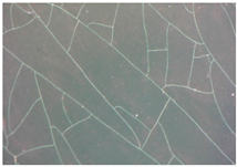
Cracks: Crack networks or delamination lines generally originate from excessive residual stress within the thin film. These stresses may be caused by thermal expansion mismatches between the film and substrate, rapid cooling, or intrinsic growth stresses resulting from high deposition rates, energetic particle bombardment, or the formation of columnar microstructures. Internal stresses from the deposition process that remain unreleased, or intrinsic brittleness of the material, may also induce cracks. When tensile stress exceeds the film’s fracture strength, cracks propagate through the coating. In contrast, compressive stress can lead to buckling and peeling.
2.3. Microscopic Thin-Film Defect Detection System
Typically, the inspection of optical films relies heavily on manual methods to select the best sample, and then test and analyze the sample. However, with the rapid advancement of artificial intelligence (AI) technologies, inspection processes have become more accurate and efficient, significantly enhancing overall productivity. This study focuses on two primary areas: detecting and classifying microscopic defects in optical thin films and optimizing deep learning models.
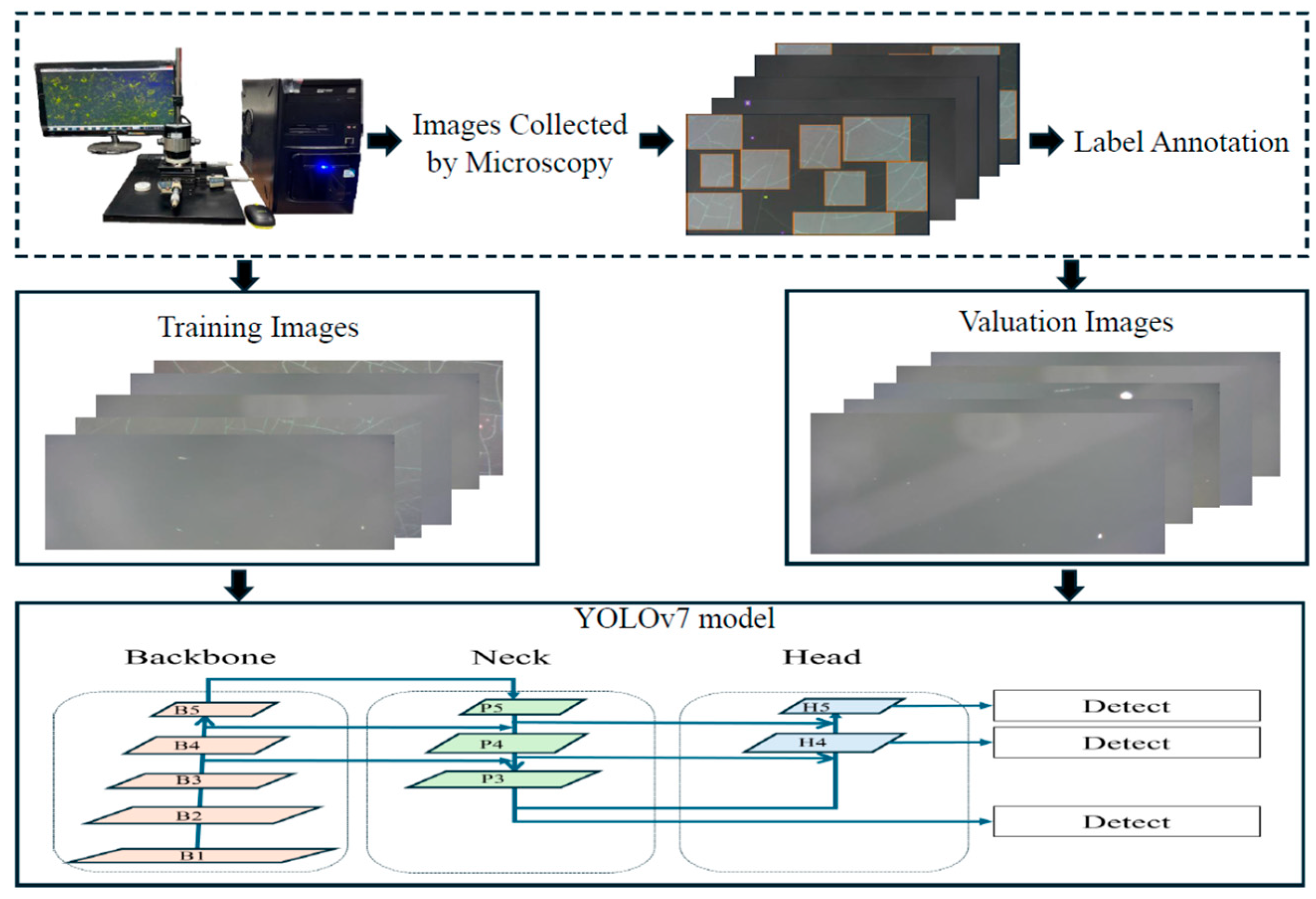
Figure 1 shows the microscopic defect detection and classification system based on deep learning and image processing techniques for thin-film coatings. The experimental dataset in this study comprises four types of microscale defects in thin films: particles, speckles, scratches, and cracks. Specifically, particles are larger, irregularly shaped entities randomly scattered across the microscopic surface of the film. Speckles are characterized by micro-holes or small grains found on the coating surface. Scratches are identified as single lines, which may be straight or curved, appearing discretely on the coating surface. Cracks define a network of multiple intersecting lines. All defect images are captured using an optical image microscope. For micro-defect classification, we use annotation software tools to label each type of defect. Subsequently, the YOLOv7 model is constructed, trained, and tested. First, the study explores the application of AI technologies to enable automated optical inspection. This includes the integration of machine learning and image processing techniques to minimize human intervention, thereby automating the inspection workflow and improving the speed and precision of defect detection. Second, the research addresses the detection of microscopic defects in optical thin films. To investigate how advanced image processing and pattern recognition methods can accurately identify and classify surface defects. Such approaches are expected to enhance product quality and manufacturing efficiency. Ultimately, the study focuses on optimizing deep learning models. This involves refining model architectures, optimizing algorithms, and enhancing training methodologies to improve the accuracy, robustness, and generalization of models applied in the context of optical thin-film defect detection. This study focuses on two primary areas: detecting and classifying microscopic defects in optical thin films and optimizing deep learning models. Research in these areas aims to enhance the accuracy and efficiency of optical thin-film inspection.
2.4. The Proposed Defect Detection Framework
Unlike the aforementioned studies, which primarily focus on defect identification and classification, the present research emphasizes optimizing deep learning models to enhance the performance of microscopic defect detection in optical thin films. This approach can achieve higher precision and robustness explicitly tailored to the unique challenges of microscopic defect inspection in thin-film coatings.
YOLO (You Only Look Once) was proposed by Joseph Redmon [
35]. It is a highly efficient object detection method based on one-stage learning. This approach integrates object classification and localization into a single neural network, allowing simultaneous prediction of object categories and bounding boxes in a single forward pass. Compared to traditional two-stage detection methods, YOLO significantly simplifies the detection pipeline by eliminating the need for region proposal generation, enabling fast and efficient detection. This makes YOLO particularly suitable for real-time applications such as autonomous driving, surveillance systems, and video analytics.
YOLOv7 [
36] was proposed by Dr. Chien-Yao Wang’s team at Academia Sinica, Taiwan. It is a leading one-stage object detection model that incorporates multiple innovative techniques, achieving notable advancements in both speed and accuracy. At its core, YOLOv7 utilizes the E-ELAN (Extended Efficient Layer Aggregation Networks) module to enhance feature fusion, thereby improving the detection of small objects and those in complex backgrounds. It also introduces dynamic label assignment, which enhances training stability in multi-object and multi-scale scenarios. YOLOv7 supports model quantization and pruning, effectively reducing memory usage and computational overhead. Furthermore, the model employs a compound scaling strategy to optimize depth, width, and input resolution, thereby enhancing adaptability across various devices.
During training, YOLOv7 employs a multi-branch architecture to enhance learning capacity. In contrast, during inference, it performs model re-parameterization to reduce computational cost without compromising performance, making it well-suited for real-time applications. On the COCO dataset, YOLOv7 demonstrates state-of-the-art performance in mean Average Precision (mAP) and Frames Per Second (FPS). The key contribution of YOLOv7 lies in its successful integration of structural innovation, training optimization, and resource efficiency. This results in an object detection framework that combines high performance, low resource consumption, and remarkable flexibility, setting a new benchmark for practical deployment and real-world applicability in object detection.
This work utilizes the YOLOv7 model, analyzing its performance across various scenarios, especially in environments that demand high performance or operate under constrained computational resources. First, image data is annotated and preprocessed, including input size adjustment, HSV color enhancement, horizontal flipping, mosaic, mixup, and paste-in enhancement strategies to improve the model’s ability to identify small defects and different backgrounds. Next, during model training, COCO pre-trained weights are used, and hyperparameters such as initial learning rate, momentum, warmup, batch size, epoch, loss weights, and IoU threshold are set. mAP, precision, and recall are monitored on the validation set to ensure convergence and stability. Finally, the deployment process converts the trained model to ONNX or TensorRT format, accelerates inference (e.g., mixed-precision FP16 or quantization), uses non-maximum suppression to remove overlapping boxes, and tests the running speed and processing capacity on actual devices to ensure the system can operate instantly, accurately, and stably in a real-world environment. We examine these models in terms of speed, accuracy, and resource consumption. Due to its efficiency and flexibility, the YOLO series has become a cornerstone of modern object detection technology, offering robust support for time-sensitive applications.
3. Experiment Details
3.1. Microscopic Thin-Film Defect Detection
To achieve efficient detection of microscopic defects in optical thin films, this study integrates high-precision image acquisition with deep learning techniques to provide a fully automated solution. Through precise microscopic imaging, the system accurately captures the micro-scale features on the thin-film surface, including the morphology and distribution characteristics of various defects. The incorporation of the deep learning model YOLOv7 ensures both high efficiency and accuracy in defect detection, while significantly reducing the time cost of the inspection process. Defect detection applies not only to laboratory testing but also enables real-time analysis on production lines, thereby playing a crucial role in enhancing the quality control of optical coating products. The following section provides a detailed description of the microscopic defect detection procedure, along with a comprehensive explanation
3.2. Pre-Processing Process of Microscopic Thin-Film Defect Images
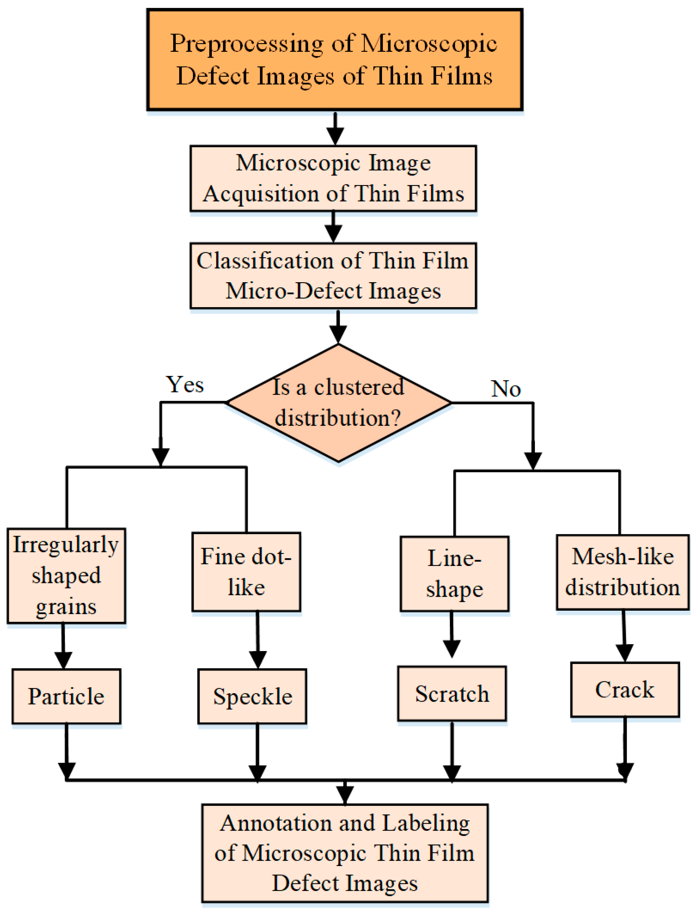
The microscopic defect detection workflow for optical thin films (as illustrated in
Figure 2) aims to achieve precise defect classification of various thin-film samples, providing an efficient and systematic inspection method to ensure quality stability during production. With the expanding applications of optical thin films in fields such as electronic components, optical devices, and semiconductor manufacturing, the accuracy and efficiency of detection technologies have become critical to safeguarding product performance.
The first step in this workflow involves placing the thin-film samples under a 500× microscopic imaging equipment to capture high-resolution images of the thin-film surface. These clear images serve as fundamental data for subsequent inspection and analysis, accurately reflecting the surface conditions of the thin films and providing a reliable basis for defect classification. Following image acquisition, defects are classified primarily into two categories based on their distribution patterns: clustered defects and network-patterned defects. This classification strategy effectively enhances inspection efficiency by accurately identifying and recording each defect type. The entire image processing workflow begins with capturing microscopic images that document the surface features of the thin films using specialized equipment. After image acquisition, the images undergo analysis and defect classification to identify abnormalities. The process first determines whether defects exhibit clustered characteristics. If so, further analysis subdivides them into speckles or particles. Speckles typically appear as distinct, minor, dot-like defects, potentially caused by internal material imperfections or external contamination.
In contrast, particles are irregularly shaped foreign bodies that often originate from external micro-debris during coating production. If the defects do not display clustered characteristics, the workflow examines whether they exhibit a network distribution pattern. Defects with such patterns are classified as cracks, typically arising from excessive internal stress in the film or thermal stress, resulting in surface fissures. If neither network patterns nor clustered features are present, the defects are categorized as scratches, which are linear damages caused by mechanical contact or friction. This classification framework accurately reflects abnormal surface features on the thin films and provides essential clues for tracing quality issues.
Upon completion of classification, all defect images are annotated and documented with detailed records of each defect’s location, type, and morphological features to ensure accuracy and traceability of inspection results. During annotation, data are formatted according to standardized protocols (e.g., saving annotations in TXT format) to maintain data consistency and quality, facilitating subsequent model training and algorithm optimization.
3.3. Model Parameter Setting and Training Process
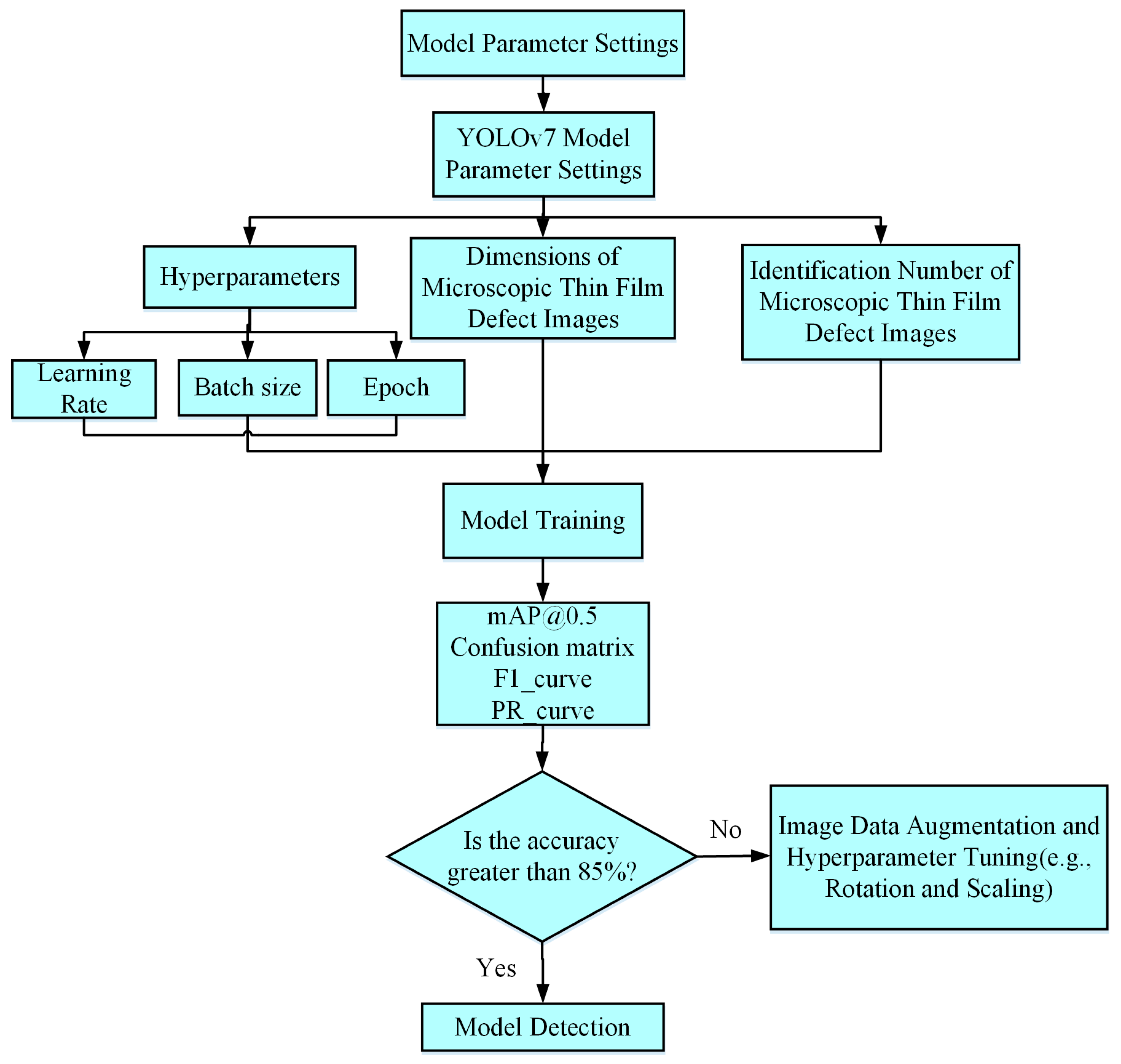
The model parameter configuration and training workflow adopted in this study, as illustrated in
Figure 3, represent a standardized procedure designed explicitly for the YOLOv7 series models. Our manual annotation and classification process for microscopic thin-film defects follows a two-level decision flow:
- (1)
Level 1 Decision for the spatial distribution (Clustered vs. Non-Clustered): First, we examine the defect’s overall distribution to determine if it exhibits “clustered characteristics”.
- (2)
Level 2 Decision (A) for sub-classification of clustered defects (Speckle vs. Particle):
If the defect is clustered, we sub-classify it based on morphology. If the features are extremely fine, fine dot-like features or micro-holes distributed in clusters, they are labeled “Speckle”. If the features are tiny, irregularly shaped grains that are typically more dispersed, they are labeled “Particle”.
- (3)
Level 2 Decision (B) for sub-classification of non-clustered defects (Mesh-like vs. Line shape): If the defect is not clustered, we proceed to the second check: does it exhibit a “mesh-like distribution”? If Yes (i.e., it forms a network structure of multiple intersecting lines with a complex shape), it is labeled “Crack”. If No (i.e., it is neither clustered nor mesh-like), it is classified as a single, discrete linear feature. These defects are typically elongated, with a length much greater than their width, and are labeled “Scratch”.
This workflow flexibly adjusts parameters to meet the demands of different application scenarios while achieving an optimal balance among model performance, accuracy, and computational resources. The overall process encompasses four main stages: model selection, parameter configuration, training monitoring, and performance evaluation, providing a comprehensive model optimization strategy.
A. Model Selection: This study employs the YOLOv7 model, primarily due to its high accuracy in object detection tasks, making it particularly suitable for scenarios that demand stringent detection precision.
B. Parameter Configuration: After selecting the model, precise configuration of training parameters is necessary, including:
- (1)
Learning Rate: Controls the rate at which model weights are updated, significantly affecting convergence speed and stability.
- (2)
Batch Size: Defines the number of samples processed per training iteration, impacting GPU memory efficiency and training speed.
- (3)
Epochs: The number of times the entire dataset is used during training, influencing the depth of learning and convergence behavior.
Additionally, to further optimize model performance, advanced parameters are adjusted based on model characteristics, such as the depth of lightweight feature extraction layers and the weighting of feature enhancement modules (e.g., Spatial Pyramid Potential, Path Aggregation Network).
C. Training Monitoring: During training, multiple key metrics are tracked in real-time to monitor learning progress, including:
- (1)
Loss function trend: Evaluates whether the model effectively learns features.
- (2)
Mean Average Precision (mAP): Reflects overall object detection performance.
- (3)
Accuracy curves for training and validation sets: Help identify potential overfitting or underfitting.
By dynamically observing these metrics, parameter adjustments can be made promptly to ensure the model converges steadily under stable conditions.
D. Performance Evaluation and Adjustment: Upon completing initial training, performance testing is conducted using four key metrics: (1) mAP@0.5; (2) Confusion Matrix; (3) F1 score curve; (4) Precision–Recall (PR) curve. If the initial accuracy of the YOLOv7 model does not reach 85%, the following optimization strategies are employed:
Data augmentation techniques (such as image rotation, flipping, and translation) are applied, fine-tuning model parameters (e.g., learning rate and batch size), retraining, and re-evaluation. This optimization cycle continues iteratively until the model performance meets the expected criteria. Finally, comprehensive validation of the optimized model is performed, including testing its stability, computational efficiency, and generalization capability across different datasets and scenarios to confirm its practicality and reliability. We set a threshold of 85% accuracy as a benchmark to guide the optimization loop [
37].
The final values of all key hyperparameters used in this study are shown in
Table 1. To achieve the high accuracy required for this study, we precisely tuned and optimized the hyperparameters of the YOLOv7 model. The selection of these parameters was based on a series of iterative experiments aimed at balancing the model’s convergence speed, accuracy, and sensitivity to minor defects such as speckles and scratches.
Table 1 details the final optimized hyperparameter values used in this work.
3.4. Microscopic Thin-Film Defect Detection
The experimental dataset in this study primarily consists of four types of microscopic defects on the thin-film surface: particles, speckles, scratches, and cracks. The definitions and characteristics of these four defect types are detailed in
Table 2. Using a microscopic film defect imaging system at a magnification of 500× (using a 50× objective lens and a 10× eyepiece), images of the four categories of microscopic thin-film defects were captured for analysis.
Various thin-film defects can severely impact the performance and reliability of thin films, potentially leading to overall failure. Particles often cause surface unevenness or structural weaknesses, undermining the film’s stability and overall quality. Speckles disrupt the uniformity of the thin films, leading to abnormal changes in their optical or electrical properties. Scratches degrade the esthetic quality and can serve as initiation sites for crack propagation, reducing the film’s durability. Cracks may rapidly propagate along internal stress concentration zones, threatening structural integrity.
3.5. Microscopic Thin-Film Defect Detection Method
This study primarily collected microscopic defect images of thin-film samples composed of various thin films, as shown in
Table 3, to enrich the dataset of thin-film defects. The microscopic defect images were acquired using an optical image microscope to capture the thin-film microscopic defects at a 500× magnification
This study divided the microscopic thin-film defect dataset into a training set of 6000 images, a testing set of 3500 images, and a validation set of 600 images to ensure data independence and diversity across model training, testing, and validation phases. Before model training, image preprocessing of microscopic thin-film defect images was critical. Image preprocessing helps clean the data, standardize image features, and reduce noise, enabling the model to focus on learning key defect characteristics.
Specific preprocessing operations included resizing images to a consistent resolution for normalization, converting images to grayscale to minimize interference from color information, and applying contrast enhancement and denoising techniques to highlight defect features. Additionally, to address the dataset’s diversity requirements, data augmentation techniques such as flipping, rotation, cropping, and illumination adjustment were employed to simulate various scenarios and enhance the model’s generalization capability.
These preprocessing procedures enhanced the learning efficiency on the training set and contributed to stable performance on the testing set, helping to prevent overfitting and underfitting. Overall, image preprocessing effectively improved the quality of the dataset.
3.6. Data Preprocessing
Data preprocessing is crucial before model training, as it significantly enhances the model’s ability to learn image features. Image preprocessing procedures include noise reduction and contrast adjustment, emphasizing defect characteristics while minimizing background interference. Additionally, appropriate data augmentation techniques, such as rotation, flipping, and scaling, are applied to enhance the model’s generalization capability.
By generating a greater variety of transformed images, data augmentation simulates diverse scenarios of microscopic thin-film defects, enabling the model to maintain high performance across different conditions. Through these preprocessing methods, the model is better equipped to identify and classify defects in thin films, thereby effectively improving detection accuracy and reliability. These techniques enhance the model’s performance on the existing dataset and strengthen its adaptability to unseen data, resulting in greater practical utility and robustness in industrial applications.
4. Results and Discussion
4.1. Results Analysis of Deep Learning Model
The results from training the YOLOv7 model enable a precise evaluation of whether the model has successfully learned the critical features of microscopic thin-film defects and can accurately classify various defect types. Specifically, we evaluate the model’s recognition capability for different defect categories by analyzing performance metrics, including Precision and Recall. Additionally, the confusion matrix provides an intuitive visualization that highlights the accuracy and potential misclassification of each defect category. These analyses help identify the model’s strengths and weaknesses, offering essential guidance for subsequent model tuning and optimization to ensure its effectiveness and reliability in practical applications. Furthermore, by examining the loss function trends during training and validation, we evaluate the model’s convergence status and detect issues related to overfitting or underfitting. Such in-depth analysis facilitates a comprehensive understanding of the YOLOv7 model performance and informs necessary adjustments and improvements.
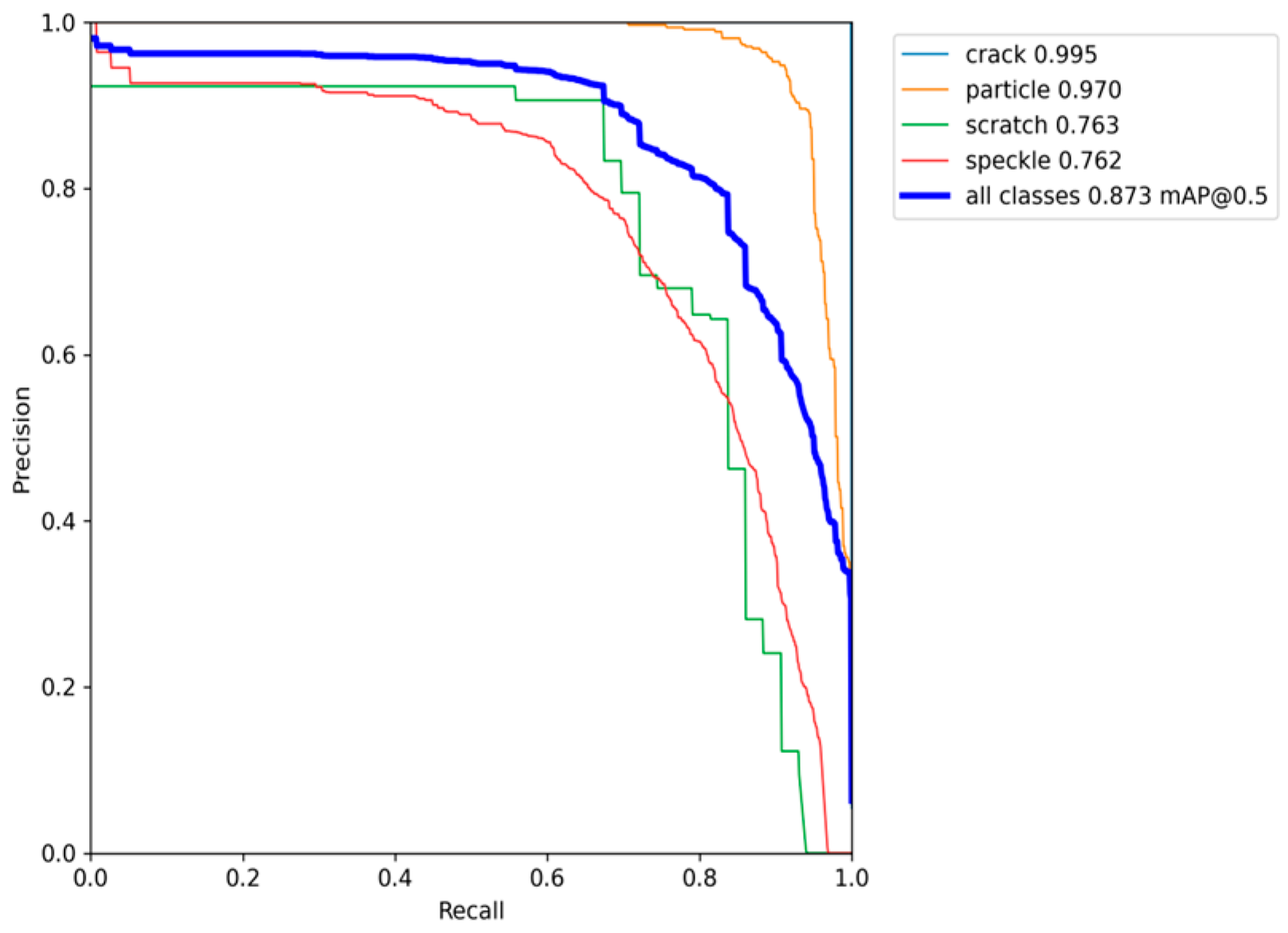
The Precision–Recall (PR) curve of the YOLOv7 model is shown in
Figure 4. The horizontal axis represents Recall, and the vertical axis represents Precision. The curve’s performance evaluates the model’s classification accuracy under varying recall conditions. The area under the PR curve corresponds to the Average Precision (AP), and the mean value of AP across all classes is the mean Average Precision (mAP), which quantifies the overall accuracy of the model. This study covers four defect categories: crack, particle, scratch, and speckle, for which individual AP values are calculated, and the weighted average of these yields mAP@0.5.
Figure 4 shows the PR curves of the YOLOv7 model, with the four defects represented by four colors. The light blue curve represents the PR curve for the crack category, which performs best, with an area under the curve close to 1 and an AP value of 0.995. This demonstrates that the YOLOv7 model has extremely high detection accuracy for the crack category, reliably identifying almost all crack defects with a very low false alarm rate, reflecting the optimization of feature learning for this category. Specific results are as follows.
- (1)
Particle (orange curve): The particle category’s PR curve ranks second after crack, with an AP of 0.970. The relatively smooth curve indicates a large area, suggesting the model’s ability to detect most particle defects accurately. However, precision slightly decreases at high recall levels, suggesting a trade-off where increasing recall may result in a slight increase in false positives for particle defects.
- (2)
Scratch (green curve): The scratch category shows moderate PR curve performance with an AP of 0.763. While the model demonstrates reasonable detection capability for scratches, precision drops notably at higher recall rates, implying that the model’s stability in learning scratch features requires further improvement.
- (3)
Speckle (red curve): The speckle category exhibits the weakest PR curve performance with an AP of only 0.762. This limitation reflects the model’s inability to detect speckle defects accurately, which can be attributed to the small size of speckle features and their low contrast against the background, resulting in higher rates of false positives and false negatives.
- (4)
All types (dark blue curve): The “All types” curve represents the model’s overall detection performance across all defect categories, with an mAP@0.5 of 0.873. This indicates that the YOLOv7 model achieves high overall accuracy but remains vulnerable to lower detection performance in the speckle and scratch categories, which prevents it from reaching the high accuracy levels observed in the crack and particle categories.
In summary, the YOLOv7 model excels in detecting crack and particle defects but shows room for improvement in identifying subtle features such as speckle. These findings suggest the need for further refinement of the model architecture and feature learning strategies to enhance overall performance.
These results from training the YOLOv7 model allow us to evaluate whether the model has successfully learned the critical features of microscopic thin-film defects and can accurately classify various microscopic defect categories. Specifically, we evaluate the model’s recognition ability for various thin-film defect types by analyzing performance metrics, including precision, recall, and F1 score.
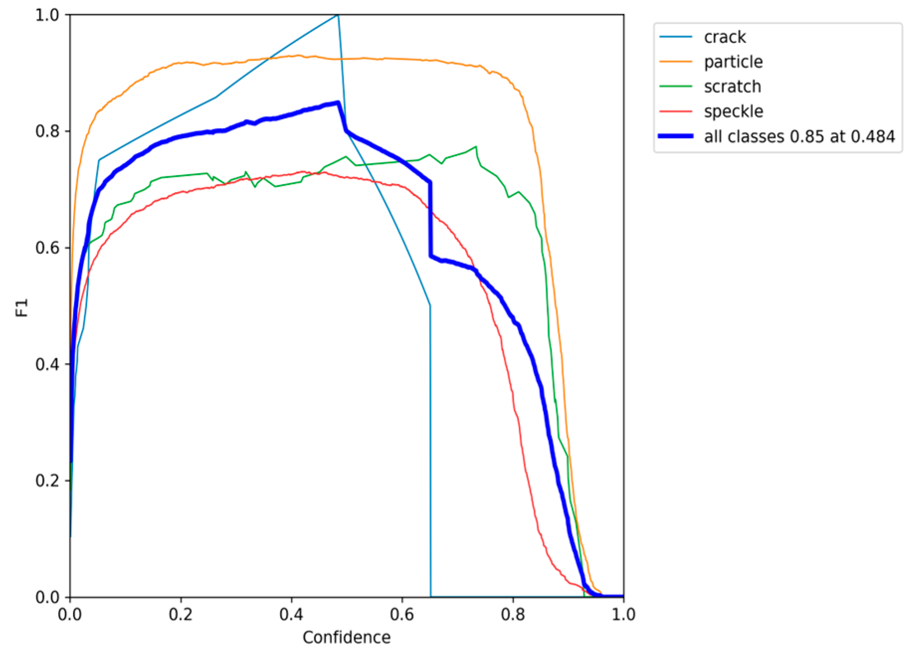
In the F1 score curve of the YOLOv7 model, as shown in
Figure 5, each curve represents the model’s detection performance (F1 score) for a specific defect category at different confidence thresholds. Significant differences in learning outcomes across categories can be observed as follows.
- (1)
Crack category (light blue): Although the crack category achieves a peak F1 score of 1.0, its curve exhibits considerable fluctuations, especially within the medium to high confidence interval (approximately 0.4–0.7). This instability may be attributed to insufficient sample size, high feature variability, or annotation inconsistencies. This indicates that while the model has strong potential in recognizing cracks, its stability requires improvement.
- (2)
Particle category (orange): The F1 curve for the particle category is generally smooth and stable, with a peak F1 score around 0.920. This demonstrates that the model effectively captures the distinctive features of this defect type. The precise shape and high contrast against the background facilitate accurate classification.
- (3)
Scratch category (green): With a peak F1 score of approximately 0.770, the model shows moderate capability in identifying scratch features. However, overall performance is limited by feature ambiguity and high shape variability, making scratches prone to confusion with the background.
- (4)
Speckle category (red): Speckle exhibits the weakest performance among the four categories, with a peak F1 score of only about 0.730. Additionally, the F1 score sharply declines at high confidence thresholds, indicating the model’s limited ability to recognize speckle defects reliably. This may be due to the tiny size and low contrast of speckle features, which reduce their separability from the background.
- (5)
All types (dark blue): The “All types” curve represents the model’s overall detection performance across all categories, with a peak F1 score of approximately 0.850 at an optimal confidence threshold of 0.484. This suggests the model achieves a relatively balanced performance across multiple defect classes at this threshold. Nevertheless, the overall F1 score is somewhat lowered by the weaker detection capabilities in the scratch and speckle categories compared to the crack and particle categories.
The YOLOv7 model performs excellently on crack and particle defects but exhibits weaker detection abilities for speckle and scratch categories. This highlights the need for further optimization in feature extraction and fine-detail recognition, including the use of data augmentation techniques, to enhance the model’s ability to learn subtle microscopic defect features. This, in turn, will improve balanced performance and overall accuracy across different defect types. These results from training the YOLOv7 model allow us to evaluate whether the model has successfully learned the critical features of microscopic thin-film defects and can accurately classify various microscopic defect categories. Specifically, we evaluate the model’s recognition ability for various thin-film defect types by analyzing performance metrics, including precision, recall, and F1 score.
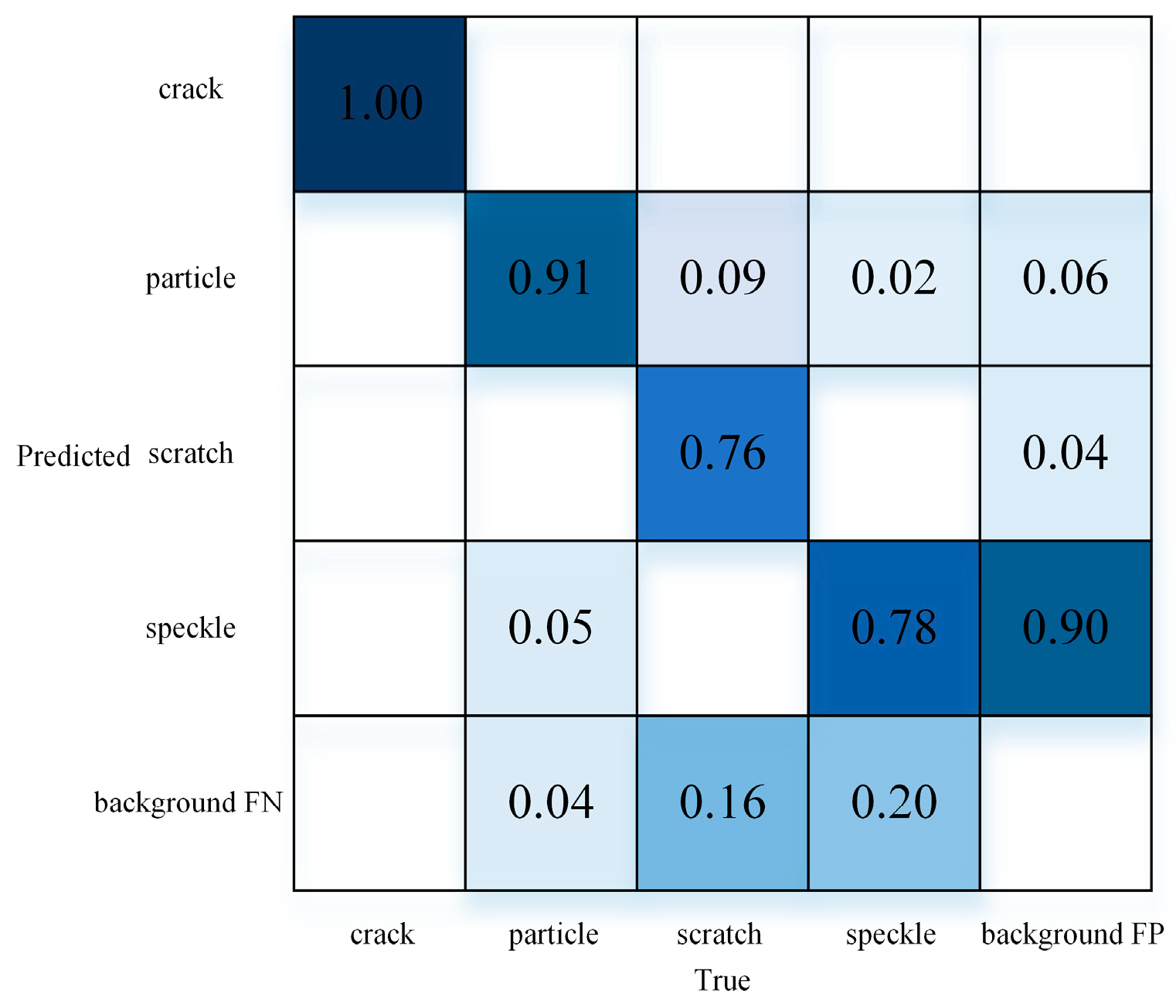
The confusion matrix is a widely used tool for evaluating classification models, particularly effective for examining model performance across different types. It is presented in a matrix form, illustrating the correspondence between the model’s predicted and ground truth labels. In object detection tasks, however, two exceptional cases arise: the model may predict a background region as an object type, or fail to detect an object altogether, classifying it as background. Consequently, the confusion matrix expands from the conventional form to a format where the additional row and column correspond to predictions and ground truths labeled as background. Since the YOLOv7 model does not generate bounding boxes for actual background regions, the intersection cell between the predicted and factual backgrounds is always zero.
From the confusion matrix of the YOLOv7 model, six distinct scenarios can be clearly observed, as shown in
Figure 6.
- (1)
For thin-film samples with accurately labeled crack defects, the model correctly predicts 100% of these as cracks.
- (2)
For thin-film samples labeled as particle defects, 91% are correctly classified as particle, five are misclassified as speckle, and four are missed entirely, being predicted as background.
- (3)
For defects in thin films, 76% are correctly identified as scratches, with 9% misclassified as particles, and 16% are undetected and predicted as background.
- (4)
For speckle defects in thin films, 78% are correctly predicted as speckle, two are misclassified as particle, and 20% are missed and predicted as background.
Overall, analysis of the YOLOv7 confusion matrix indicates that the model exhibits the strongest recognition capability for the crack category, achieving a perfect accuracy of 100%. In contrast, the classification accuracy for categories such as speckle and scratch is relatively lower. Notably, the model predicts speckle defects as background in 20% cases, indicating a tendency to miss these finer features and confuse scratches with background regions.
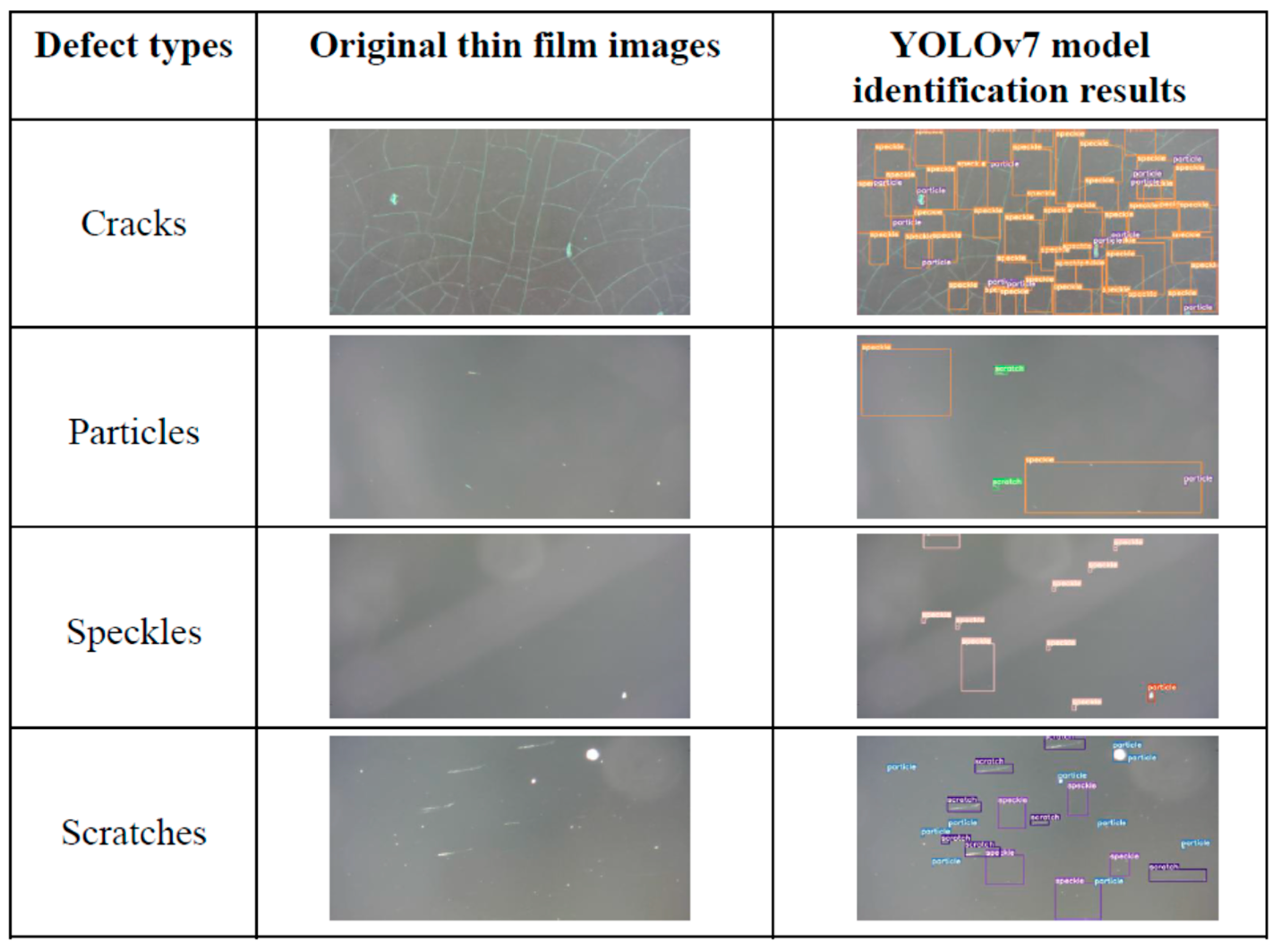
The specific results of the YOLOv7 model for microscopic thin-film defect recognition are illustrated in
Figure 7.
Figure 7 reveals that the YOLOv7 model can accurately identify and classify defects across various categories, including cracks, particles, speckles, and scratches. Notably, the model demonstrates exceptionally high accuracy in detecting cracks, with almost no false positives or false negatives.
For particle detection, the YOLOv7 model reliably identifies the majority of particle distributions; however, a small number of false detections still occur in regions with complex backgrounds. In contrast, the recognition accuracy for speckle and scratch categories is relatively lower, especially for speckle defects, where some instances remain undetected, indicating the model’s limited capability in handling fine-grained features.
Overall, the YOLOv7 model demonstrates robustness and superiority in terms of detection accuracy and feature learning. Nonetheless, further optimization is required to enhance performance in atom-scale features or scenarios with high background interference. These findings provide a foundational reference for subsequent model improvements and underscore the pivotal role of YOLOv7 in microscopic thin-film defect detection tasks.
4.2. Deep Learning Model Analysis and Discussion
In this section, we provide an analysis and discussion of the YOLOv7 model’s performance at the data level. As an object detection architecture known for its high model capacity and structural complexity, YOLOv7 excels in evaluation metrics such as mean Average Precision (mAP). To further evaluate its potential applications, this study investigates the model’s detection performance across various scenarios, with a particular focus on the influence of background complexity and the distribution of defect features on accuracy. Experimental results show that even in situations with complex background textures or unclear defect boundaries, the YOLOv7 model maintains a stable recognition capability, achieving a mAP of 87.3. This reflects its strong feature extraction ability and robust generalization performance.
An analysis of the confusion matrix reveals that the model tends to misclassify defects as background in images with complex backgrounds, leading to false negative detections. The main reasons for this issue are likely the lack of distinctive features for the defects, which makes it difficult for the model to differentiate them effectively, and the need for further optimization of the model’s algorithms. To address this problem, enhancing the unique characteristics of various microscopic thin-film defect features during training could help the model learn these features more accurately. Additionally, improvements in training methodologies and algorithm design are needed.
