Article

Preparation of Very Thin Zinc Oxide Films by Liquid Deposition Process: Review of Key Processing Parameters

1
Unité de Recherche Matériaux & Ingénierie Mécanique, Université de Reims Champagne-Ardenne, CEDEX 2, 51687 Reims, France
2
Laboratoire de Physique de la Matière Condensée, Université de Picardie-Jules Verne, CEDEX 1, 80039 Amiens, France
*
Authors to whom correspondence should be addressed.
Coatings 2022, 12(1), 65; https://doi.org/10.3390/coatings12010065
Submission received: 13 December 2021 / Revised: 31 December 2021 / Accepted: 2 January 2022 / Published: 6 January 2022
(This article belongs to the Collection Feature Paper Collection in Thin Films)

Abstract

:
We used sol-gel and spin-coating in the original configuration of a liquid deposition process to synthesize particularly thin ZnO films (<100 nm) with nano-granular morphology, high grain orientation and variable optical properties. The concentration of the zinc salt, the concentration of the chelating agent, the nature of the solvent and the substrate material have been identified as key parameters that determine the microstructure of the deposited layer and thus its final properties. The thorough and practical examination of the effects of the synthesis parameters evidenced a three-step growth mechanism for these ZnO thin films: (i) a reaction of precursors, (ii) a formation of nuclei, and (iii) a coalescence of nanoparticles under thermal annealing. The growth of these very thin films is thus conditioned by the interaction between the liquid phase and the substrate especially during the initial steps of the spin coating process. Such thin ZnO films with such nano-granular morphology may be of great interest in various applications, especially those requiring a large active surface area.

1. Introduction

Zinc oxide (ZnO) is a well-known material for its large spectrum of interesting properties and possible applications [1,2,3,4,5,6]. Actual or potential devices applications include solar cells [7,8,9,10,11], photocatalysis [12,13,14,15,16], piezoelectric nanogenerators [17,18], UV light emitters [19,20], transparent transistors [21,22], memory devices [23,24], acousto-optic devices [25,26] and gas sensors [27,28]. These various applications require the control of the layer morphology from a microscopically homogeneous and flat surface to a nanoscale designed surface.
Previously ZnO thin films have been manufactured with various methods including magnetron sputtering [29], pulsed laser [30,31], molecular beam epitaxy [32], atomic layer deposition [33], chemical vapor deposition [34] and spray-pyrolysis [35]. Among these numerous elaboration methods, sol-gel coupled with spin-coating offers some advantages such as low-cost, large-scale deposition, facilities availability and morphology changes. However, the obtained film morphology and properties strongly depend on the elaboration recipe, the chemical reactants, the elaboration conditions and the thermal treatment. To control the film properties, it is necessary to understand the growth mechanism and its effects on the observed properties.
It is known that thin films properties and morphology can be affected by post-processing annealing temperature, which has been the subject of several works. In the case of the sol-gel spin coating technique, the morphology and properties of the film are also impacted by processing parameters such as the chelating agent [36,37], the zinc salt concentration [38,39,40], the solvent [41,42,43,44,45], the rotation speed [46,47,48,49,50,51,52,53,54,55,56,57] and the nature of the substrate [58,59,60,61,62,63]. In the present study, spin coating, which is usually devoted to the spreading of viscous solutions, is used in an uncommon configuration of fluid liquid deposition, giving rise to very thin films (<100 nm) with peculiar nano-granular morphologies. Therefore, the strong constraining contribution of the liquid-substrate interaction in the case of very thin films enhances the effects of the different key deposition parameters. In previous works, we have discussed the growth [64] of these nano granular ZnO thin films and in particular the role of the film thickness in such process [65,66]. In this paper, we further investigate the effects of preparation parameters and discuss the mechanisms of deposited film formation. The results of this study will help define the optimal conditions for obtaining high quality thin films for potential applications such as photocatalysis [67].
In order to emphasize the effects of key deposition parameters on the morphological and structural properties in the early stages of ZnO film deposition, we chose to perform this work under the following conditions:
(i)
a low viscosity liquid precursor solution to better highlight the substrate-solution interaction;
(ii)
a successive deposition of layers of a few nm thickness to obtain a ZnO film whose thickness does not exceed a hundred nm;
(iii)
an annealing temperature allowing to obtain a nanogarnular structure of excellent crystal quality.

2. Experimental Details

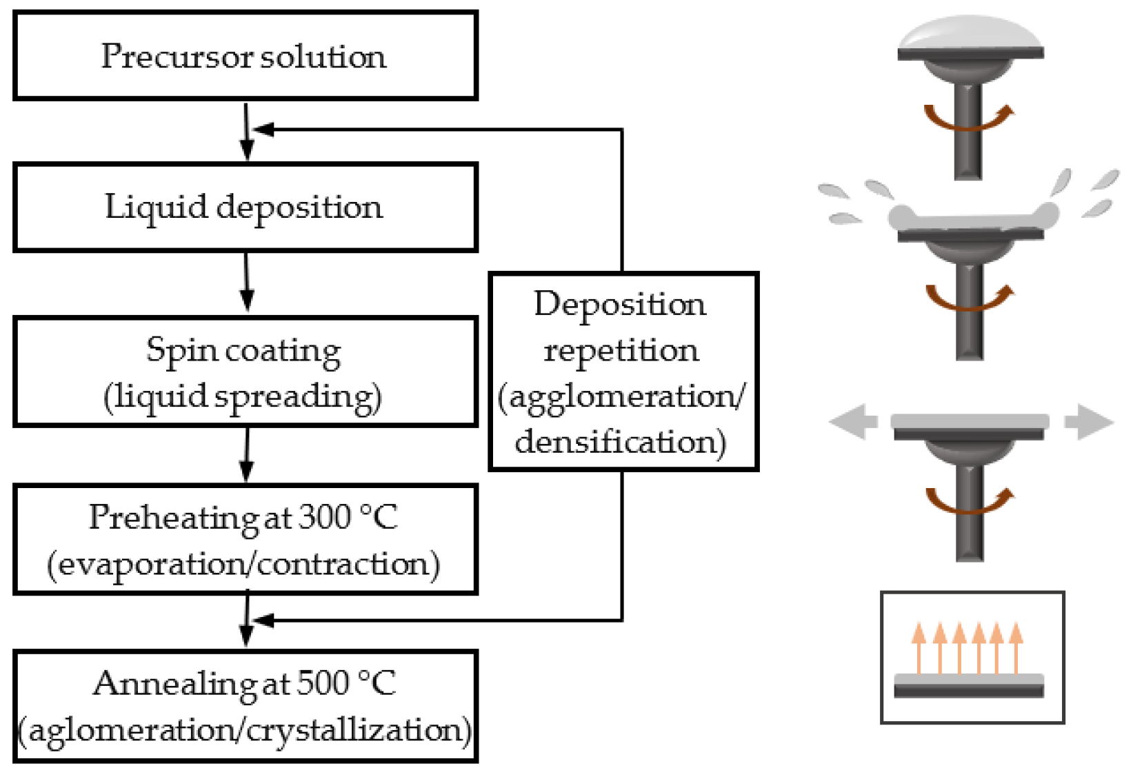
2.1. Sol-Gel Spin-Coating Deposition Process

The elaboration of very thin layers by liquid phase deposition and spin-coating is based on the process shown in the diagram of Figure 1. The liquid phase, consisting of the suspension of ZnO precursors, involves the dissolution of zinc acetate dehydrate (ZnAc, Zn(CH3CO2)2·2H2O) in various solvents using monoethanolamine (MEA, C2H7NO) as a chelating agent. The mix is then stirred for 30 min to completely dissolve the zinc acetate. At the end of this stage, a clear and transparent ZnO precursor solution is obtained. After 24 h aging, the layers are elaborated using a repetitive deposition process. In the deposition step, droplets of the liquid precursor solution are shed on the substrate, previously cleaned first by ethanol then by acetone and finally with de-ionized water and rotated at the desired speed with an acceleration time of 20 s. At the end of the rotation process, the liquid is spread over the whole substrate forming a very thin film which is then put in a furnace (Nabertherm, Lilienthal, Germany) at 300 °C to evaporate solvents. Our previous works have established that the deposition and drying process must be repeated at least four times to obtain a dense granular thin film [64,65]; and that the post-processing annealed in air at 550 °C for 1 h is adequate to lead a good crystallization [68]. Apart from the two stages of preheating and annealing, the entire process takes place at room temperature.

2.2. Spin-Coating Rotation Speed

The morphology of the ZnO film results from the tuning of many chemical and physical parameters including the concentration and nature of the reagents, the rotation speed, the spreading time, the substrate characteristics, the drying and annealing temperatures. Especially, the rotation speed is known to have various effects on grain size [49,50], roughness [46,47,48,49], orientation [50,51,52], stoichiometric composition [51], thickness [48,51,52,53,54,55] and electrical performances [52,56,57]. However, these effects are expected to be changed in the case of liquid spreading, as the centrifugal force has the double effect of first spreading the liquid into a very thin liquid film and then ejecting the excess liquid from the substrate. In order to properly select the spin-coating speed we deposited ZnO thin films at different rotation speeds ranging from 500 to 4000 rpm. Above a rotation speed of 1500 rpm, the ZnO thin film becomes homogeneous with only very narrow iridescent edges due to the different deposition cycles (Figure 2a). Its thickness and optical and crystallographic properties also remain unchanged with rotation speed. Below 1000 rpm, the deposited film shows a yellow square homogeneous central part with irises around it, resulting from incomplete spreading of the liquid during the spin-coating process (Figure 2b). Under these conditions of deposition from a liquid (hence with a low viscosity), it is though that only the limit boundary tension between the substrate and the liquid is reached to give rise to a very thin, homogeneous and continuous film of ZnO above 1500 rpm.

2.3. Substrate Shape

Although the spin-coating process is known to be a technique transportable to a large-scale deposition, the effects of the substrate size and shape have rarely been studied. The known effects only concern an increase in cracks, in the case of samples of a few tens of cm2 during the liquid phase deposition [49]. The substrate size and shape have been carefully chosen by elaborating samples with a length from 10 to 40 mm and a length to width ratio from 1 to 2. Samples as small as 10 mm in size are affected by relatively large edge effects (Figure 2c), while samples up to 40 mm in size show some small spots due to the liquid retraction during the evaporation process. In addition, the length to width ratio should not exceed 2, as the liquid spreading into a very thin homogeneous liquid film requires the symmetry of samples. In the present work, a typical size of 20 mm × 20 mm is chosen to obtain samples free of cracks with a nano-granular structure.

2.4. Standard Deposition Conditions and Processing Parameters Variations

After setting the rotation speed and substrate size, the study focused on the effects of the ZnO precursor concentration, the chelating agent content, the substrate type and the solvent nature. In the field of very thin layers, these parameters have indeed proved to be key parameters affecting the liquid-substrate interaction during the deposition process. We have defined as standard conditions the following processing conditions: a zinc acetate concentration [ZnAc] of 0.5 mol/L, a chelating agent content r = [MEA]/[ZnAc] of 1.0, 2-methoxyethanol as the solvent, a rotation speed of 2500 rpm and a 50 nm SiO2 covered crystalline silicon (SiO2/c-Si) as a substrate. Then four sets of samples are considered by varying (i) the reagent concentration [ZnAc] between 0.25 and 1.50 mol/L, (ii) the chelating agent content within the range 0 ≤ r ≤ 2.0, (iii) the solvent nature (2-methoxyethanol, ethanol or propanol) and (iv) the substrate type (c-Si, SiO2/c-Si or float glass). In the results section, each parameter that has changed compared to the standard conditions is systematically specified. The repeatability of the process was tested by checking measurements on at least three samples for each set of deposition parameters. The error bars shown are the standard deviation evaluated on this set of similar samples.

2.5. Characterization Techniques

The characterization of the film morphology was carried out by a cross-sectional view performed with a Raith field emission gun scanning electron microscope (SEM, Raith, Dortmund, Germany) operating at 5.0 kV. The characterization of the surface topography has been carried out with a Digital Instruments nanoscope III atomic force microscopy (AFM, Digital, CA, USA) in the tapping mode. The AFM micrographs recorded on the 1 μm × 1 μm area provided the AFM values for: (i) the lateral grain size and (ii) the maximum peak to valley height which represents the depth separation between the grains. The characterization of the crystal orientation has been carried out with a Bruker D5 X-ray diffraction (XRD, Bruker, MA, USA). XRD spectra of ZnO thin films present only significant contribution in the 30°–40° of 2θ range, showing peaks pointing at 31.770°, 34.422° and 36.253°, respectively attributed, according to the Joint Committee on Diffraction Powder Standards (JCPDS) 36-1451 of bulk ZnO, for 100, 002 and 101 orientations, respectively. The spectra present the dominant 002 peak, revealing the Wurtzite phase of ZnO with c-axis perpendicular to the substrate plane. Crystallite size (D) was calculated by Scherrer formula:
D = 0.9 λ β cos θ
where λ is the X-ray diffraction wavelength, β represents the full width at half maximum and 2θ is the diffraction angle that defines the crystalline orientation of the ZnO thin film.
The optical characterization was carried out with a Jobin-Yvon Uvisel UV-visible spectroscopic ellipsometer (SE, Horiba, Palaiseau, France) in the range 1.5–5 eV at an incident angle of 70°. Ellipsometry measures the change of polarization state between incident light and reflected light on a sample, resulting from multiple reflections due to the thin film structure and optical properties of the media and interfaces. SE measurements were treated assuming a representative bi-layer optical model with a bulk ZnO layer (with a thickness db) and a top roughness layer (with a thickness ds) and using an original inversion process described elsewhere [68,69,70] to extract db and ds as well as the complex dielectric function ε = εr + i of the deposited ZnO material. The surface roughness layer is considered to be formed by 50% of the same material as the bulk layer and 50% of void (εV = 1).
Moreover, since the nano-granular material is always less dense than the perfectly crystalline material, residual porosity is detected through the reduction of the magnitude of the dielectric function of the bulk layer compared to that of the reference crystalline material. An effective porosity of the bulk layer can be estimated using the effective medium approximation [71]. Thus, its dielectric function ε is modeled by an effective medium consisting of a dense reference ZnO material [72] with a dielectric function εref and a void volume fraction fV representing the material porosity:
f v ε v ε ε v + 2 ε + ( 1 f v ) ε r e f ε ε r e f + 2 ε = 0

3. Results and Discussion

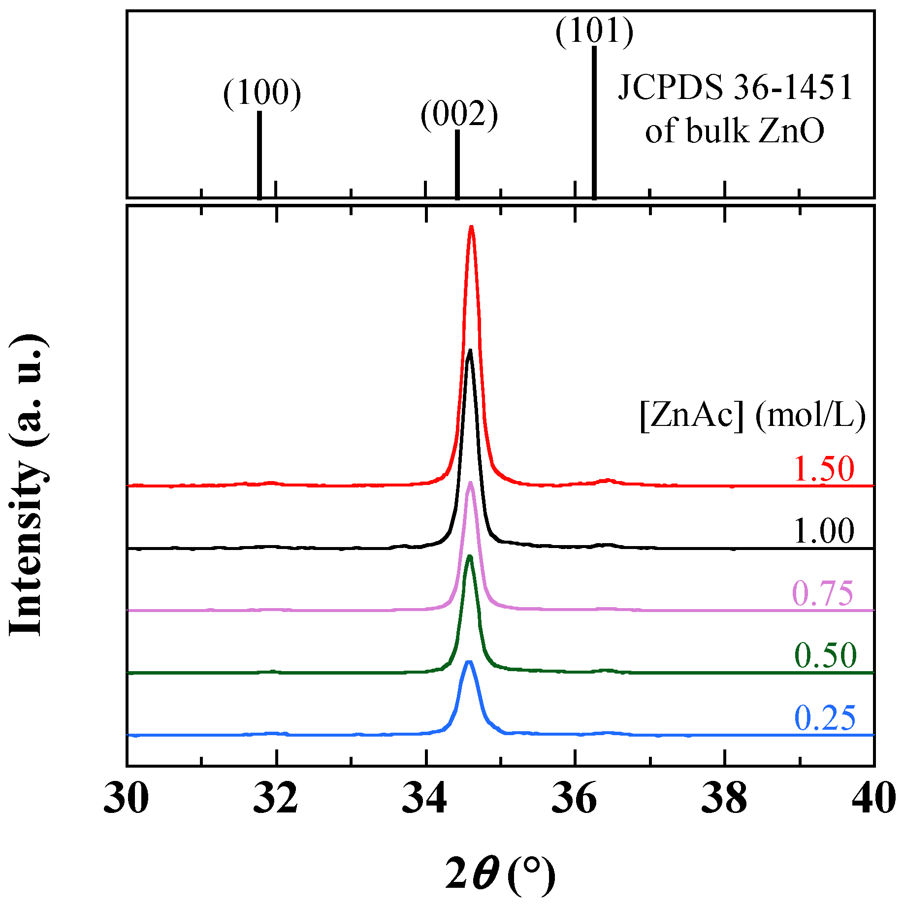
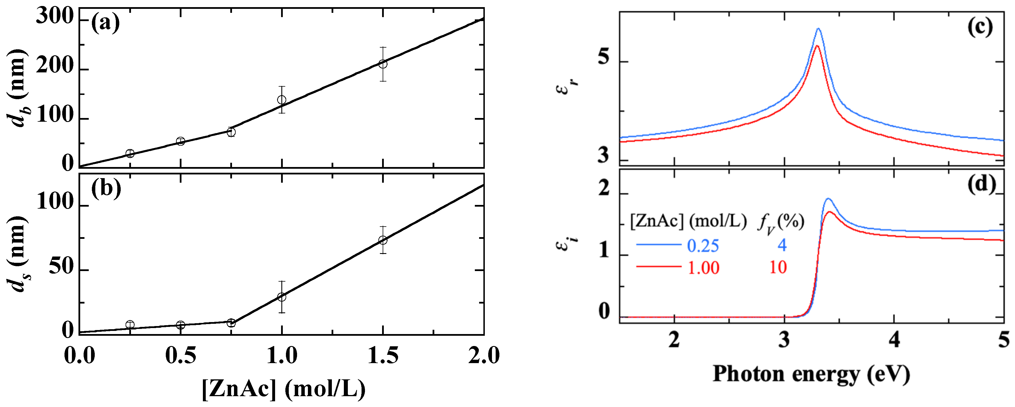
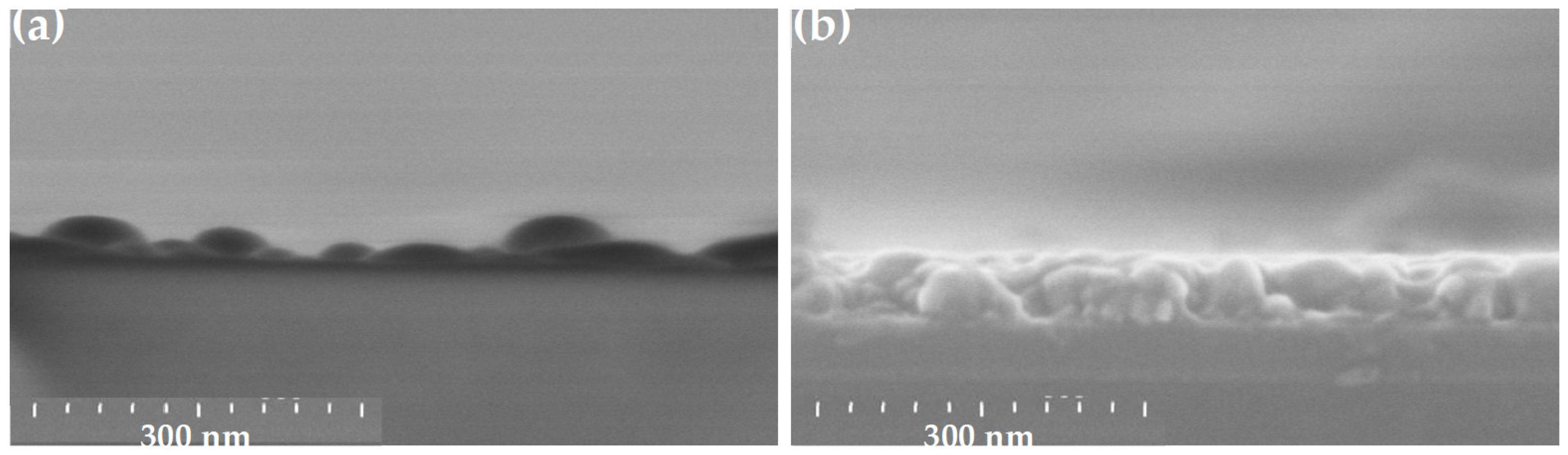
3.1. Effects of the ZnO Precursor Concentration

The effects of the ZnO precursor content were investigated against standard conditions by varying zinc acetate concentration ([ZnAc]) between 0.25 and 1.50 mol/L. The first expected effect of increasing the amount of material with [ZnAc] is an increase in the deposition rate and thus the thickness of the deposited ZnO film. This effect is immediately visible through the appearance of the film. Its color changes from blue (Figure 2a for [ZnAc] = 0.50 mol/L) to shiny yellow (Figure 2d for [ZnAc] = 1.00 mol/L) as a result of the film thickness increase.
The depth film morphology of ZnO film is shown in Figure 3 for two representative cases: a low concentration [ZnAc] = 0.25 mol/L (Figure 3a) and a high concentration [ZnAc] = 1.00 mol/L (Figure 3b). The morphology of grains closely packed together is obtained in both cases, with a grain size increasing with the reagent concentration. Moreover, small grains, at low [ZnAc], lead to apparently a more homogeneous film, while large grains at high [ZnAc] make the surface rougher.
The granular morphology of ZnO thin films observed by AFM is shown in Figure 4a,b for [ZnAc] = 0.25 and 1.00 mol/L, respectively. The AFM lateral size and height for the whole concentration set are plotted in Figure 4c,d, respectively. The grain size gradually increases from a value of 30 to 60 nm. The AFM height linearly increases from 20 to 80 nm within the studied reagent concentration range.
The crystalline quality observed by XRD spectra is shown in Figure 5 for samples obtained with various ZnAc concentrations. All the ZnO films prepared with different concentrations exhibit the high intensity (002) peak. For all these samples the ratio of (100), (101) peaks to the intensity of the (002) peak is less than 10−2, which attests the good orientation of the prepared material according to the c-axis perpendicular to the surface of the substrate. As the ZnO precursor content increases, the (002) peak intensity is enhanced in agreement with the increase in the thickness of the deposited layer (see Figure 6a). The crystallite size given by Equation (1) shows a slight increase in the 30–40 nm range with the reagent concentration, suggesting that the large grains result in fact from the agglomeration of crystallites.
The thickness of both the bulk layer (db) and the surface roughness (ds), derived from SE measurements, are displayed in Figure 6a,b, respectively. The thickness db gradually increases from 30 nm to 220 nm when [ZnAc] increases from 0.25 to 1.50 mol/L with a clear acceleration from 0.75 mol/L. Up to [ZnAc] = 0.75 mol/L, the surface roughness remains very low (≤10 nm). Beyond that, ds increases considerably to reach 70 nm at high concentrations (≥1.00 mol/L).
The spectra of the real (εr) and imaginary (εi) parts of the dielectric function of the deposited material are shown in Figure 6c,d, respectively. We have restricted the presentation to two extreme values of [ZnAc] for readability, not to overload the figures. εi shows the bandgap peaking step near 3.4 eV (Figure 6d), related to the strong excitonic absorption, with transparency below the bandgap, attesting of the good crystal quality. εr is determined by Kramers-Kronig relations (Figure 6c). The effective porosity associated with the dielectric function amplitudes evolves from 4% to 10% by increasing [ZnAc] from 0.25 to 1.50 mol/L. The increase in porosity is due to grain size (Figure 3b and Figure 4b), as the smaller the grains the denser the structure.
In summary, for low and moderate concentrations ([ZnAc] ≤0.75 mol/L), ZnO samples become very thin films with a smooth surface, good crystalline quality, and small grain size. For high concentrations ([ZnAc] ≥1.00 mol/L), ZnO samples display a good crystalline quality but a large grain size and a rough surface. The concentration of zinc acetate is a fundamental parameter in the synthesis of ZnO films. This parameter influences the crystallographic orientation of the grains and it has been reported that a concentration higher than 0.50 mol/L can alter the crystalline quality [38,39,40,52,73,74,75,76,77,78]. This does not seem to be the case for our films, probably due to particular formation mechanisms and their very small thickness.
The granular morphology is the consequence of a continuous coarsening process during the different stages of preheating and final annealing. Large grains are formed by the agglomeration of small grains under the effect of thermal energy. Indeed, the relatively high preheating temperature (300 °C) allows a fast evaporation of the solvent and then colloidal movement until agglomeration by contact. The final annealing step (550 °C) provides additional thermal energy to induce structural and morphological modifications, improvement of the crystallization and additional cluster coarsening or agglomeration [79,80,81]. At low ZnAc concentration, the substrate attraction should enhance the nucleation of small particles over the entire substrate surface. The combination of these small grains under thermal excitation forms a dense layer. A high ZnAc concentration promotes a rapid formation of large grains by agglomeration of small grains with large grains. Since the large and heavy grains have a reduced mobility, the resulting film has thus little opportunity for further relaxation, and is, therefore, of lower density.

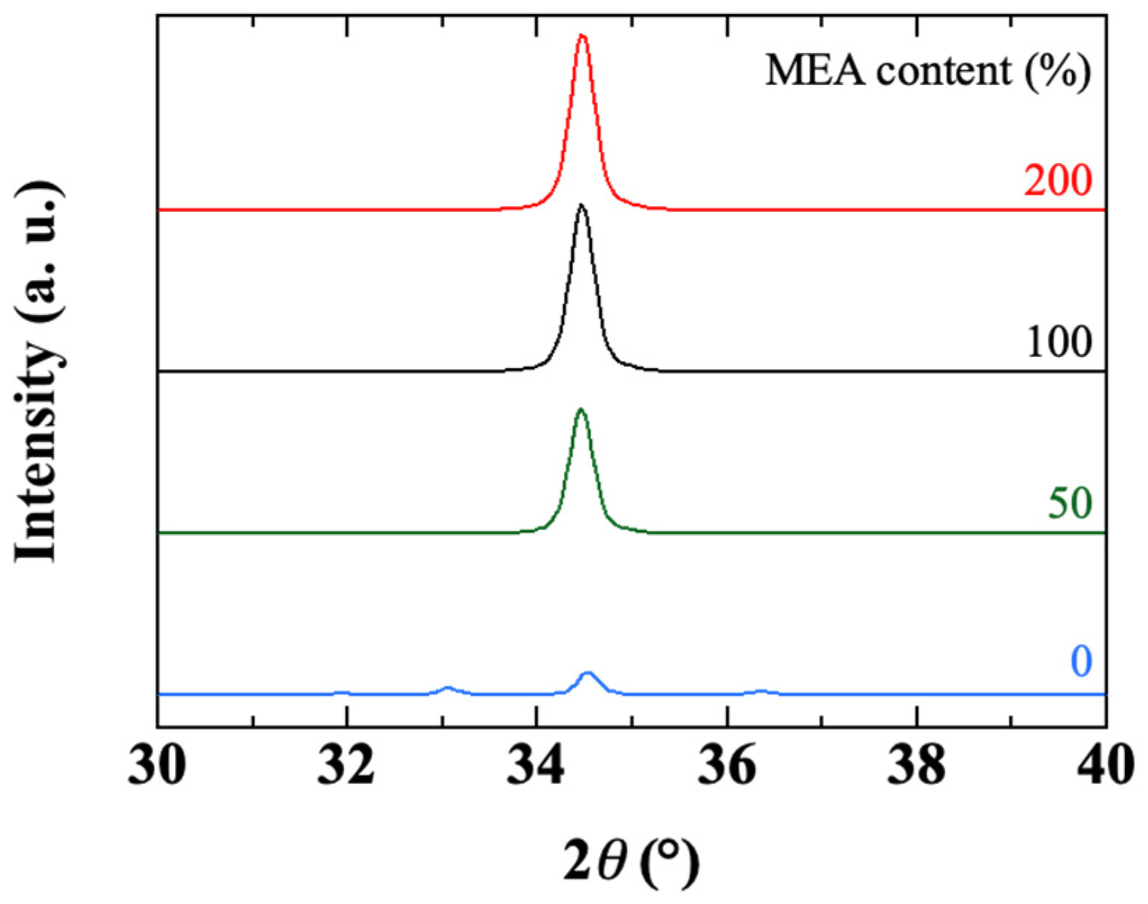
3.2. MEA Content Effects

MEA content effects were compared to the standard conditions by varying the ratio r = [MEA]/[ZnAc] from 0 to 2.0. Without MEA (r = 0), the partial dissolution of ZnAc reduces the deposition rate and leads to inhomogeneous films with disturbed areas due to undissolved salt crystals. Note that, in this case, the measurements were limited to the homogeneous parts of the deposited film. For 0 < r ≤ 1.0, the ZnO film surface is homogeneous (Figure 2a). Beyond, the film shows uncoated small spots (Figure 2e).
Figure 7 shows the depth layer morphology of ZnO thin films in the case of r = 0 (Figure 7a) and r = 1.0 (Figure 7b, standard sample), respectively. Without the chelating agent (r = 0), the very inhomogeneous and thin film is difficult to study. The SEM image of Figure 7a shows an irregular microscopic morphology with scattered grains. The samples deposited with r > 0 show a well-stacked grain morphology (Figure 7b).
The AFM micrographs of Figure 8a,b confirm the granular morphology of the ZnO thin films obtained both without (r = 0, Figure 8a) and with MEA (r = 1.0, standard sample, Figure 8b). The samples are typically made of grains with particularly smaller size without the chelating agent. In this case, the sample has a different morphology, as it is not completely homogeneous and has a very small thickness. AFM data for the entire MEA content are shown in Figure 8c,d. The lateral dimension, close to 20 nm without MEA, grows to about 40 nm for high MEA contents (Figure 8c). At the same time, the AFM height, of about 25 nm without MEA, rapidly reaches about 45 nm in the presence of MEA (Figure 8d).
The XRD spectra of samples obtained with various MEA contents are shown in Figure 9. We previously mentioned the fact that without the addition of the chelating agent (r = 0), the deposited film was much thinner and inhomogeneous (Figure 7a and Figure 8a). Figure 9 shows that the crystallinity of the sample is also affected. Except for this particular case, Figure 9 indicates that the MEA content does not really seem to affect the crystallographic structure and structural properties of the deposited ZnO film. Whatever the MEA content (r > 0), the obtained ZnO film shows a high intensity (002) peak and an intensity ratio of the (100), (101) peaks with respect to the (002) peak lower than 10−2, which proves the good crystalline orientation of the material along the c-axis perpendicular to the substrate surface. Moreover, the size of the crystallites deduced from the (002) peak by Scherrer’s formula is always close to 35 nm.
The thickness of the bulk layer and the roughness layer, deduced from SE the measurements, is shown in Figure 10a,b. The absence of a chelating agent (r = 0) reduces the adhesion of the liquid to the substrate during the spin-coating process leading to a very thin film. For MEA content such as 0.5 ≤ r ≤ 2.0, both the bulk layer and the surface roughness keep an almost constant thickness, in the range of 50–70 nm and 5–15 nm, respectively.
The spectra of the real and imaginary parts of the dielectric function of the films deposited at different MEA contents are shown in Figure 10c,d, respectively. Without MEA (r = 0) the dielectric function spectrum shows a reduced intensity of the excitonic peak and a reduced amplitude due to a large effective porosity of 32%. Such a high effective porosity is attributed to the very small thickness on the one hand and the inhomogeneities with a large number of uncovered areas of the substrate on the other hand (Figure 7a, Figure 8a and Figure 10a,b). By increasing the MEA content, the effective porosity of the material decreases to 8% beyond r = 1.0. The overall results highlight the direct effects of MEA content on the thickness, morphology and optical properties of the deposited ZnO film. In particular, the ZnO thin film deposited without MEA (r = 0) differs from the others because of the incomplete dissolution of zinc acetate. Various effects are attributed to the chelating agent (MEA), including the dissociation of zinc acetate in the solvent, formation and stabilization of the ZnO colloidal solution [37,82,83,84] and the coordination of metal atoms [82,85], as well as consequences for microstructure and optical properties [36,37]. Furthermore, in the case of very thin films, as the chelating agent directly affects the chemistry of the precursor solution, it also indirectly affects the liquid deposition on the substrate and the formation of ZnO nuclei in the preheating step.
The ZnO precursors are likely to take different forms depending on the used reactants and conditions [73,74,86,87,88,89], including, for instance, colloidal particles [79,80], zinc acetate sheets [90] or zinc oxo-acetate precursor [73], deposited either as a continuous gel layer or pre-formed colloidal particles. Different chemical mechanisms have been proposed to explain the ZnO formation, including the zinc monoacetate formation and complexation with the chelating agent [91], the zinc hydroxide formation and condensation [92], or the possible formation of the zinc hydroxy double salt [93,94]. In these reactions, the effect of amino-additives is evidenced to influence ZnO properties [73,95,96]. Especially the presence of the MEA chelating agent can induce a Zn-MEA complex formation.
Based on infrared spectroscopy measurements of the present ZnO precursor solution, probable mechanisms of the present reactions can be described in a few steps. First, zinc acetate dihydrate molecules dissociate in the alcohol into mono-acetate ions thanks to water molecules [36]. Then the stoichiometric reaction between monoacetate ions and MEA yields Zn-MEA complexes [91,92]. After 24 h of solution rest, this complex dissociates to molecules of zinc dihydroxide Zn(OH)2 and MEA molecules back with water. In summary, one mole of each reagent (ZnAc and MEA) gives one mole of zinc hydroxide. If MEA concentration is lower than ZnAc concentration, the dissociation of monoacetate will only be partial and the zinc dihydroxide concentration will be lower than the ZnAc concentration. If MEA concentration is higher than that of ZnAc, a total dissociation of zinc monoacetate becomes possible, while MEA excess molecules remain unused, which is consistent with similarities of ZnO layer properties when r ≥1.0.

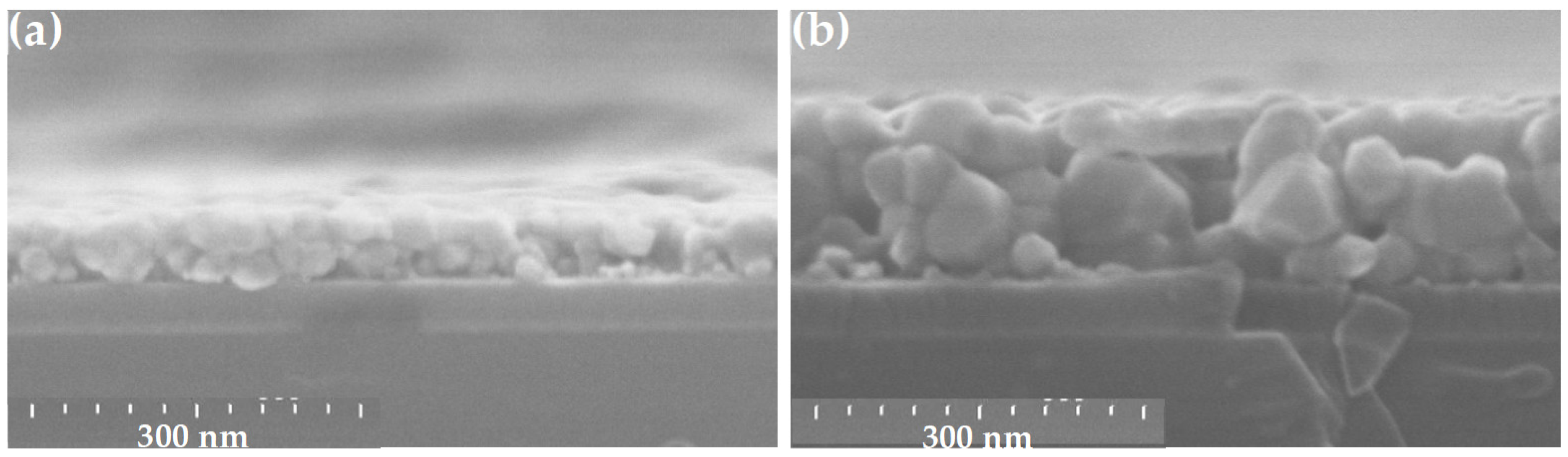
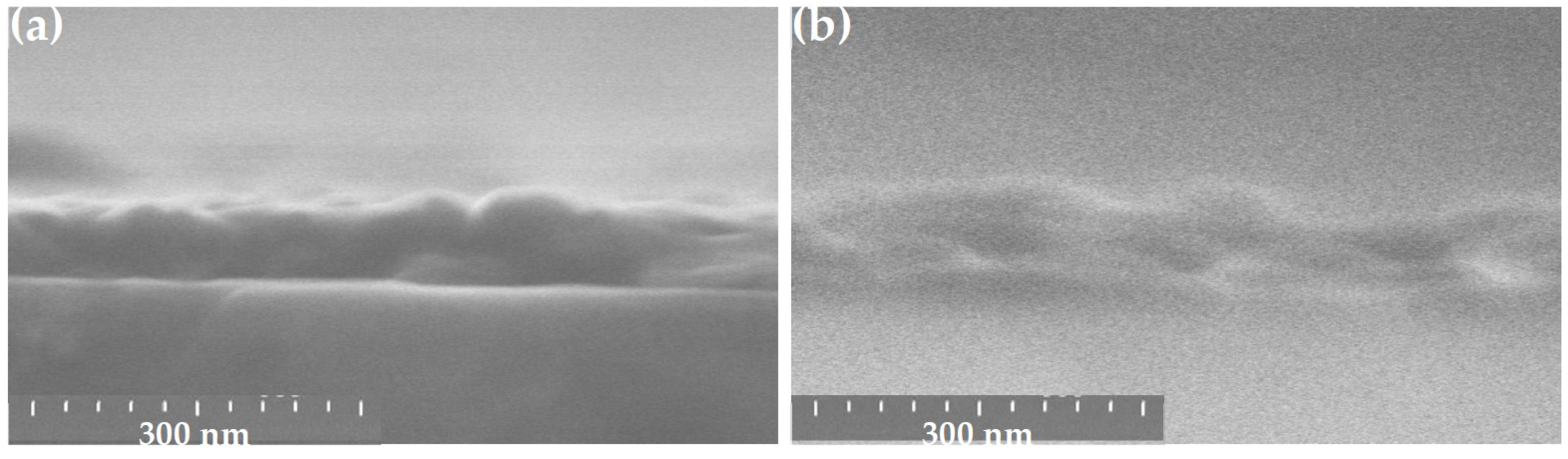
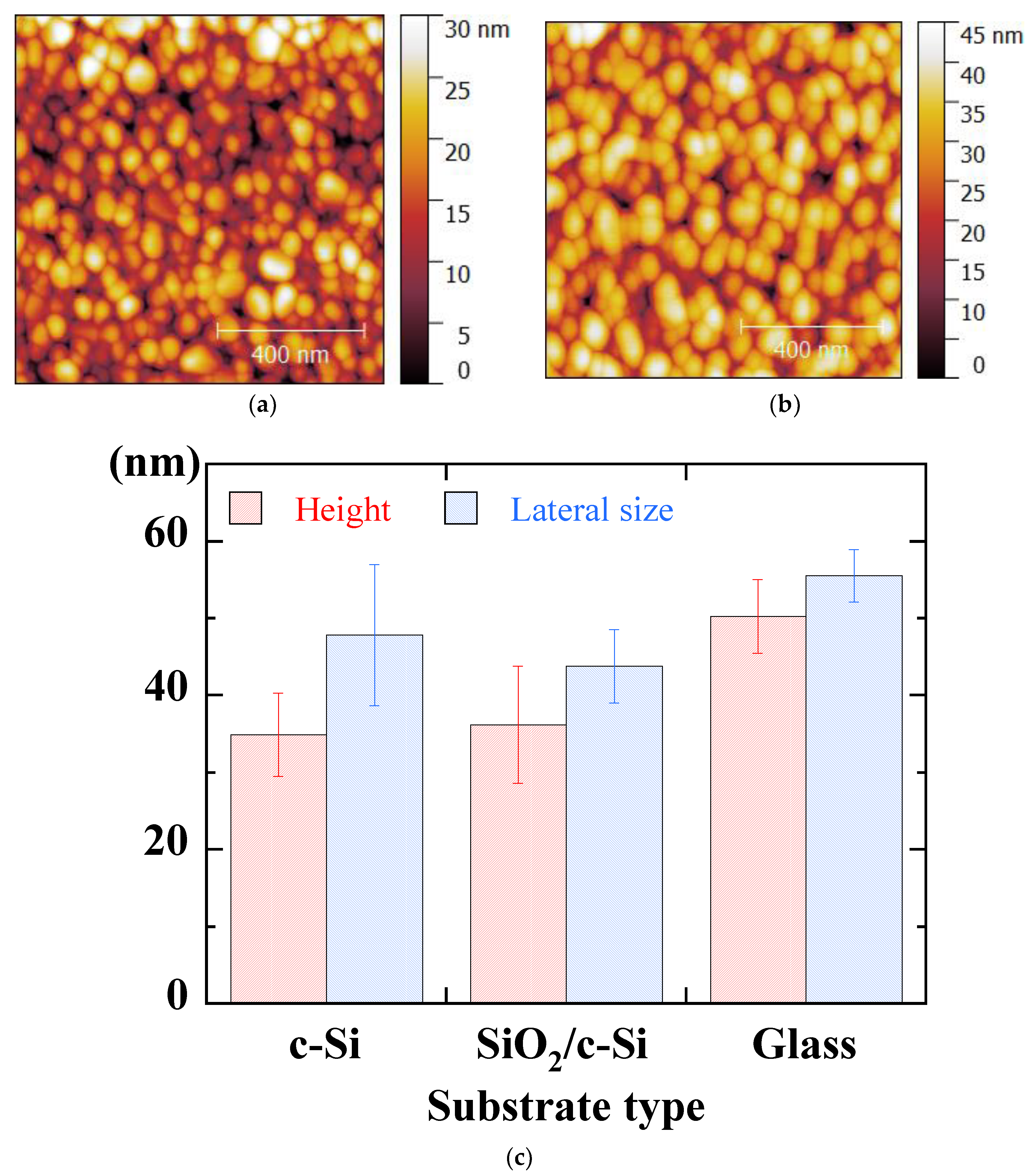
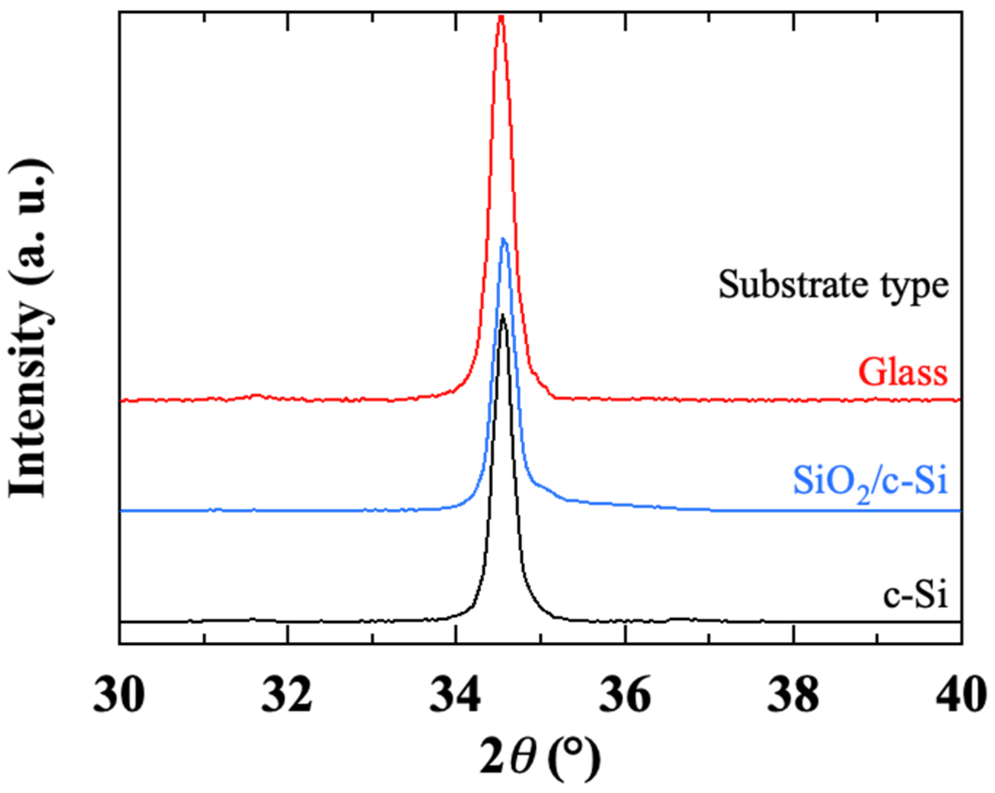
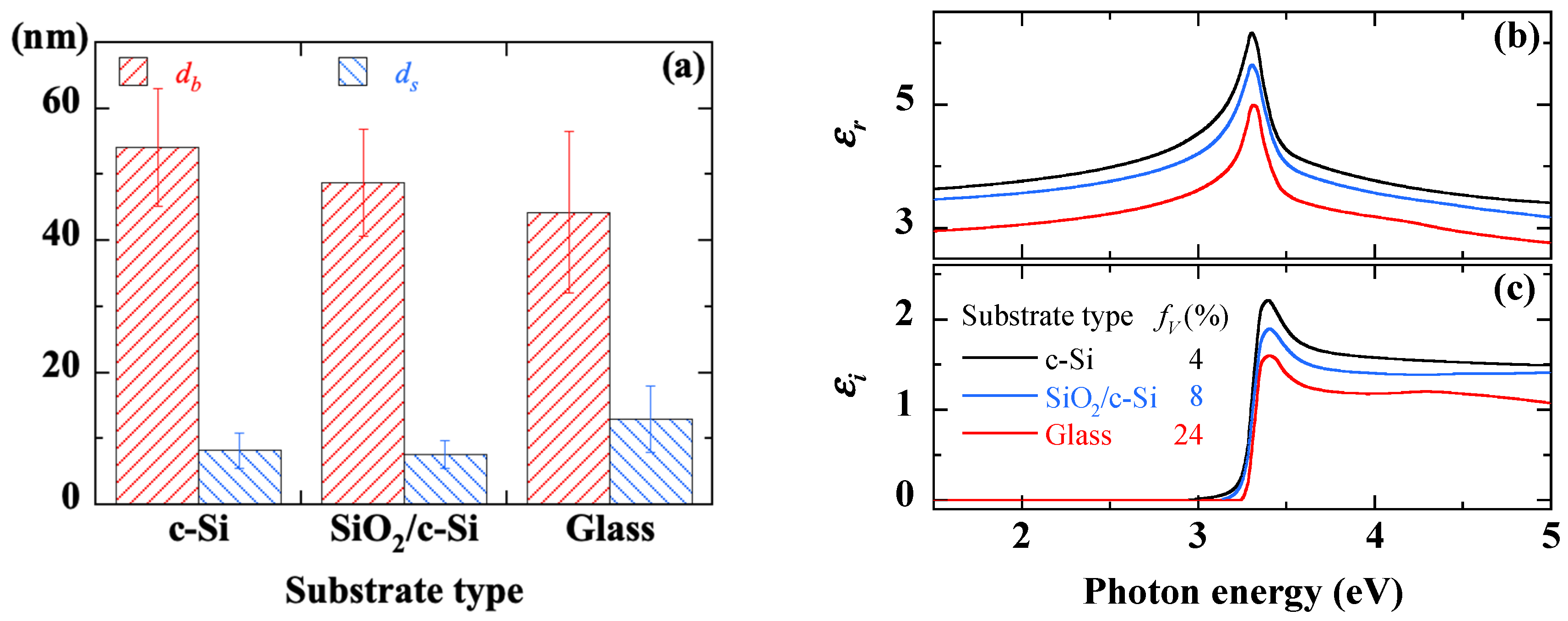
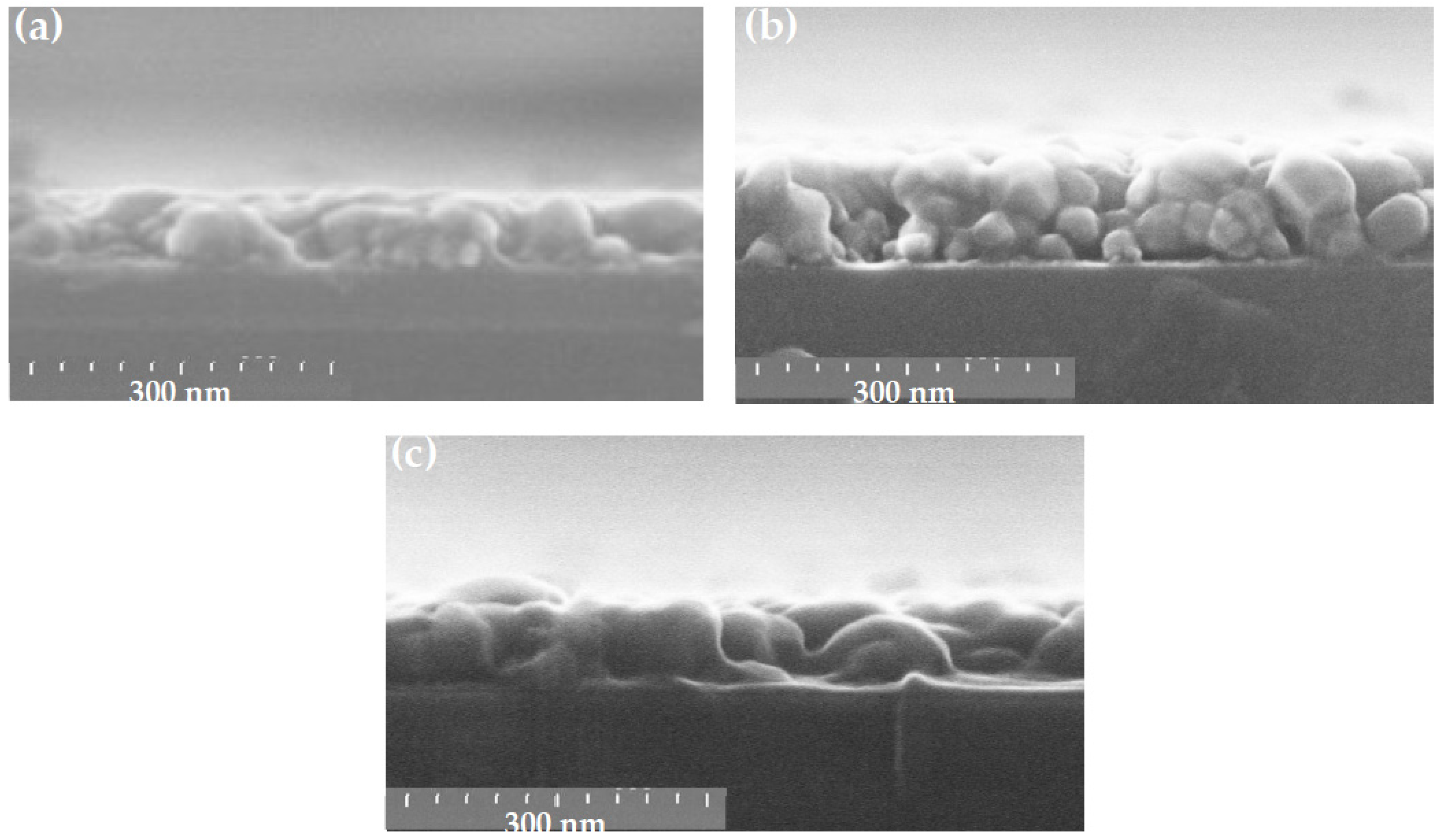
3.3. Effects of the Substrate

ZnO thin films were deposited under standard conditions on three types of substrates: c-Si, SiO2/c-Si, and glass, leading to a homogeneous film regardless of the substrate type. Figure 11 shows the cross-sectional SEM images of ZnO films deposited on c-Si (Figure 11a) and glass substrate (Figure 11b), respectively. They present the morphology of grains closely packed together. The films deposited on SiO2/c-Si and c-Si substrates show a similar grain morphology with grains separated by small voids. In the case of a glass substrate (Figure 11b), the sample exhibits a different granular structure with separate larger grains presenting a rounded top shape leaving more voids between them.
AFM micrographs of ZnO thin films deposited on c-Si and glass substrates are shown in Figure 12a,b, respectively. These images show a very similar grain morphology. Figure 12c summarizes the AFM data (lateral size and height) for all the substrates we tested. The lateral size increases from 45 nm for the SiO2/c-Si and c-Si substrates to 55 nm for the glass substrate. The AFM height increases from 35 nm for the SiO2/c-Si and c-Si substrates to 45 nm for the glass substrate. In the case of glass, the morphology can be thought to be different with a structure of larger grains separated by large voids.
Figure 13 displays the XRD spectra of ZnO thin films on various substrates. The spectra show a strong peak (002) and an intensity ratio of peaks (100) and (101) to peak (002) of less than 0.01, indicating a very good orientation of these samples with the c-axis perpendicular to the substrate surface. Peak (002) gives, according to Scherrer’s formula, a crystallite size of about 35 nm in the case of both SiO2/c-Si and c-Si substrates, but about 30 nm for the glass substrate. This result implies a weak epitaxial effect due to crystalline silicon. The crystalline or amorphous state of the substrate surface may therefore influence the liquid-substrate interaction during the deposition of the first layer.
The results derived from the SE measurements are displayed in Figure 14. The roughness (ds) remains less than 10 nm for all the samples (Figure 14a). The films deposited on both SiO2/c-Si and glass substrates have a similar thickness of the bulk layer (db) in the range of 50–55 nm, whereas the film deposited c-Si exhibits slightly higher thickness (Figure 14a). These slight variations in thickness would be due to differences in interaction between the substrate and the liquid during the first moments of deposition.
The dielectric function spectra of ZnO material are shown in Figure 14b,c. The variation of their amplitude reflects the fact that the effective porosity increases from 4% to 8% and then to 24% when the film is deposited on c-Si, SiO2/c-Si, and glass substrate, respectively. In agreement with SEM observations of Figure 11b, the deposition on the glass substrate leads to a relatively large porosity due to the film microstructure made of relatively large grains separated with voids. The agglomeration process seems to be different in the case of the glass substrate, maybe because of its amorphous structure that affects the interaction between the ZnO nanoparticles and the substrate surface.
The previous results converge towards the conclusion that the substrate nature has significant effects on the characteristics of such very thin films. Many works have reported the effects of the substrate material on the orientation [58,59,60,61,62], grain size [58,63], emission [59] and morphology [59,60] of ZnO thin films. These effects are more significant in the case of very thin films. Indeed, the substrate influences the microstructure of the film, during the first moments of the deposition, by the adhesion of the liquid film during the spin coating steps, and by the agglomeration and the densification of the precursors during the successive steps of heating and annealing. The substrate/particles interface can be influenced by the substrate, as crystalline silicon shows dipoles formed by the native dioxide silicon thin layer [97], while glass contains rather unoriented polar molecules. The zinc dihydroxide precursor being a polar molecule, its interaction with the substrate can be thought of as Van Der Waals forces whose energy (Evdw) is given by:
E v d w = A 12 π d 2
where d is the film thickness and A is the Hamaker constant depending on the three environments (substrate, precursor, and the air). If A has a negative value, the interface interactions are repulsive. If A has a positive value, the interface interactions are attractive. When the precursor is deposited on a very well-ordered surface such as c-Si, the surface dipoles attract the precursor dipoles, so that the adhered dipoles will be ordered and densely packed. In the case of an amorphous substrate (glass), the precursor dipoles are accumulated on the substrate surface with random orientations, so that nucleation is started in an unpacked system. The amorphous nature of glass reduces the attraction between the nuclei and the substrate surface in favor of the interaction between the grains, so that the grains can preferably agglomerate in the lateral dimension to form larger structures but separated by voids, maybe leaving some free substrate surface spots.
In addition to particles/substrate interactions, the liquid/substrate interaction is expected to have a large influence on the film growth. The wettability of the different substrates was additionally investigated. For that purpose, contact angle measurements were performed on both c-Si and glass substrate with a goniometer (DSA 30, Krüss, Nürnberg, Germany), using distilled water as liquid. Before each measurement, the sample was cleaned in successive ultrasonic baths with acetone and distilled water. A drop of 2 μL in volume is deposited on the surface of the substrate using a syringe. A photograph of this drop taken with a charge coupled device (CCD) camera a few seconds later gives a contact angle of 60° in the case of c-Si and 40° in the case of glass. This measurement confirms the more hydrophilic character of glass which may also contribute to weaker substrate/liquid interaction.

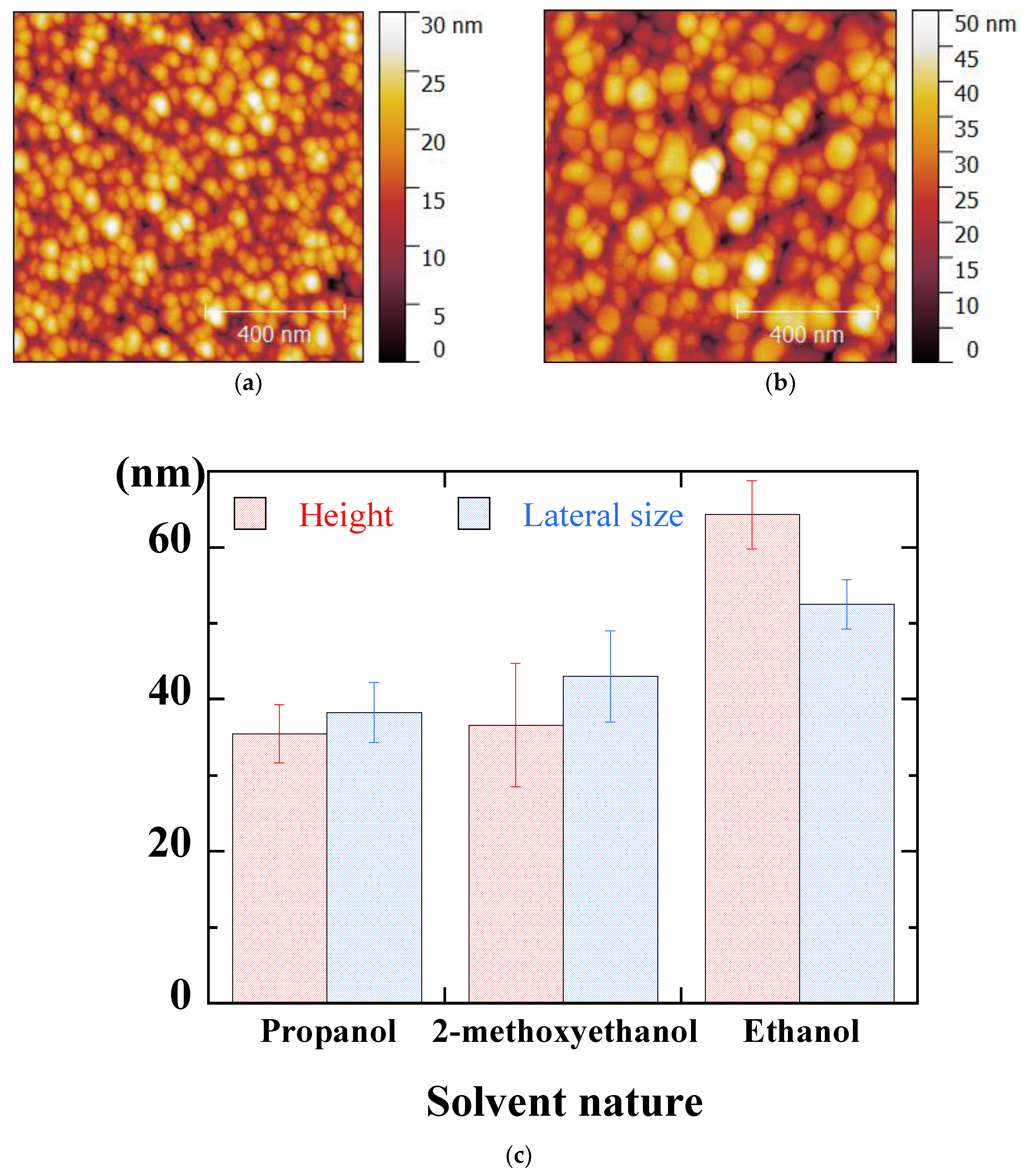
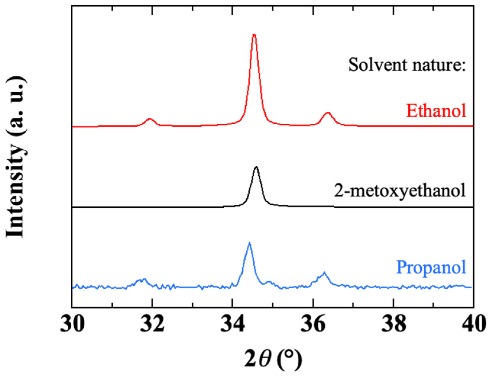
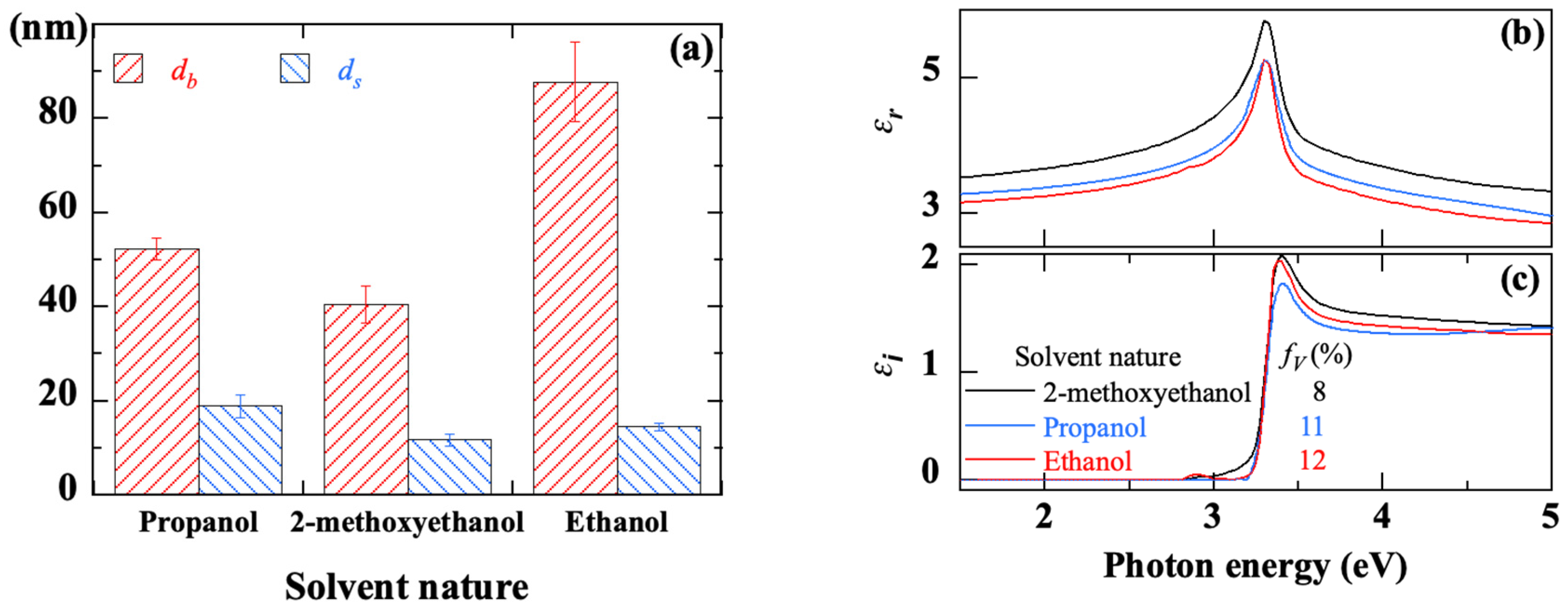
3.4. Effects of the Solvent Nature

We have experimented the deposition of ZnO thin film against standard conditions using the following three solvents: 2-methoxyethanol, ethanol and propanol. The ZnO thin film obtained with the most volatile solvent (ethanol) has a brighter appearance (Figure 2f). This is due to the progressive evaporation of the solvent during the deposition, which artificially increases the precursor concentration and consequently increases the thickness compared to that obtained with the two other solvents as is shown in the cross-sectional SEM views of Figure 15. Although the samples appear to have a similar granular morphology, the nature of the solvent clearly influences the thickness of the film obtained as well as its surface roughness. Ethanol (Figure 15b) produces the thickest film with large agglomerates of grains separated by large faults, compared to the ZnO layer developed by the solvent 2-methoxyethanol (Figure 15a). With propanol (Figure 15c), the sample also has large grains, which appear to be distributed in a sort of monolayer in direct contact with the substrate and separated by voids. In the case of 2-methoxyethanol (Figure 15a), the sample grains are smaller, which allows them to be arranged in a dense layer under the effect of thermal annealing.
Figure 16a,b show AFM micrographs corresponding to samples elaborated with propanol and ethanol, respectively. The samples present similar granular aspects with, nevertheless, a significant difference in terms of grain size. In the case of ethanol (Figure 16b), the resulting film is porous with large grains. This could be an advantage in applications requiring a reactive surface grade such as photocatalytic activities. The AFM data (lateral size and height) for the different solvents are summarized in Figure 16c. The lateral size, around 45 nm using 2-methoxyethanol or propanol, grows to 55 nm with ethanol. The AFM height increases from 35 nm with 2-metoxyethanol and propanol to 60 nm with ethanol, in agreement with the increase in film thickness (see Figure 15), which will also be confirmed by ellipsometry measurements. The particular morphology, with large voids between neighboring grains, obtained in the case of ethanol (Figure 16b) would be a consequence of a relatively high deposition rate, which would favor the formation of large grains to the detriment of a relaxation of agglomerates and a densification of the layer.
The XRD spectra of ZnO thin films obtained with various solvents are displayed in Figure 17. The sample obtained with 2-methoxyethanol shows a high-intensity (002) peak with almost no (100) and (101) peaks. Using propanol or ethanol, peaks (100) and (101) appear on either side of the high-intensity (002) peak, suggesting a lower crystallinity quality. The intensity ratio of the (100) peak to the (002) peak is 0.2 for propanol and 0.1 for ethanol, whereas it is less than 10−2 for 2-methoxyethanol. Using the (002) peak, Scherrer formula gives a mean crystallite size of around 35 nm for all solvents.
The results derived from SE measurements are shown in Figure 18. The thickness of the bulk layer, quite close to 50 nm with both propanol and 2-methoxyethanol, increases considerably to about 90 nm using ethanol (Figure 18a). For all samples, the roughness below 20 nm is indicative of good surface quality (Figure 18a). The spectra of the real and imaginary parts of the dielectric function of ZnO thin films made with the three different solvents are shown in Figure 18b,c, respectively. The excitonic peak is slightly higher in the case of 2-methoxyethanol, in agreement with a higher crystallographic quality, in comparison with propanol or ethanol. The porosity increases from 8% with 2-methoxyethanol to 11% and 12% with propanol and ethanol, respectively. Such porosity would be relative to the voids between grains in the case of a coarse-grained sample.
The effects of the solvent on the crystalline orientation of the ZnO film [41], its morphology [42], its electrical [43], photocatalytic [44], or photovoltaic [45] performances, have already been reported. Indeed, the solvent may not only be involved in the chemistry of the precursor solution [49,91,98,99,100] but it may also affect the interaction between the liquid and the substrate during the spin-coating process. In the present process of deposition from a liquid phase, the solvent is involved mainly through two of its intrinsic properties: its boiling point and its polarity. The boiling point is a key parameter in the preheating stage. The boiling points of ethanol, 2-methoxyethanol and propanol are, respectively, 78, 125 and 98 °C. During preheating, the solvent evaporates to form ZnO grains by agglomeration of the precursors. Thus, the higher the boiling point of the solvent, the slower its evaporation will be, leading to a better crystallinity of the ZnO thin film. The polarity of the solvent can also have significant effects on the structure of ZnO [101]. The XRD results in Figure 17 indicate that films synthesized with 2-methoxyethanol (with a dipole moment μ = 2.04 Debye) have better crystallinity with a strong (002) orientation. The presence of (100) and (101) peaks in the case of films obtained with propanol (μ = 1.86 Debye) or ethanol (μ = 1.66 Debye) reveals a rather polycrystalline structure. A solvent with a high dipole moment and a high boiling point leads to dense films with better crystallinity. Conversely, a solvent with a low dipole moment and low boiling point can induce enough disorder during the film growth process, which combined with rapid growth can prevent any relaxation and densification of the film. These effects are probably the reason for the increased porosity observed in the case of ethanol, without excluding other possible chemical interactions due to the solvent.

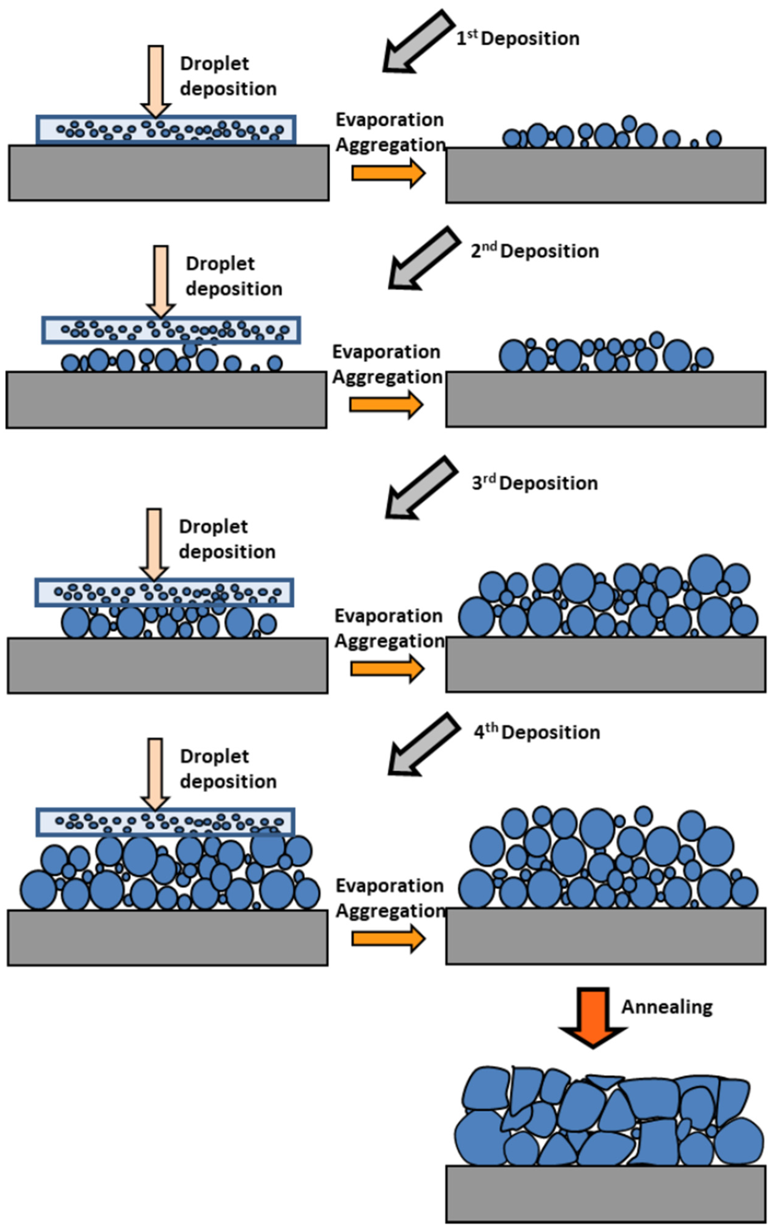
4. The Genesis of a Very Thin ZnO Film

In previous works, we conducted a study on the growth of ZnO by spin-coating under the same original liquid deposition conditions, varying the thickness of the thin film between 20 and 120 nm and studying the evolution of its morphology [64,65,66]. This study allowed us to propose a growth model for the material. The current study allows us to refine this model and to examine the influence of different key parameters. In the following, we will discuss the growth process of these very thin films taking into account the different mechanisms related to sol-gel.
The morphology of sol-gel ZnO thin films is generally granular [102,103,104,105,106] or columnar [106,107,108], by coarsening or maturation of smaller particles during the preheating [75,109,110] or heating [79,104] steps. Some more particular transformations can be observed: (i) from grains to more complex objects such as nanorods [111]; (ii) from a vertical to a lateral geometry [108,112,113] probably involving nuclei as a former layer for a self-template growth until coalescence [108]; (iii) from a granular to a columnar structure by the continuous growth of grains assisted by an enhanced diffusion process [80]; or (iv) from glassy plate surface to nano-grain or nano-needle shape by contraction of zinc acetate sheets to form polynucleous precursors [90]. In the formation of dense films, dipole-dipole interaction between the polar nano-grains is the process most commonly cited to explain the self-assembly growth of highly c-axis oriented ZnO thin films [114].
The present study concerns very thin films with only granular morphology with different grain sizes and void contents. The growth process is then assumed to be based on a simple mechanism of core formation and grain coarsening under thermal excitation, with increased contributions from substrate/precursor and substrate/grains interactions. Starting from the initial chemical reactions leading to the formation of the ZnO precursor in the solution, the genesis of the formation of the ZnO film would consist in the following sequence of steps schematically represented in Figure 19.
(i) Nuclei Formation. ZnO precursors in solvent suspension are spread over the substrate surface by spin-coating. The evaporation of the solvent during the preheating step at 300 °C allows the formation of small grains by aggregation of the precursors. It can also result in additional heat-induced chemical reactions. These nuclei might be ZnO molecules or small colloids obtained after a heat-activated evaporation of the solvents, by transformation or agglomeration [75,114,115]; or by a self-template process [108]; or by acetate decomposition and crystallization [75,81,82]. In the present very thin films, we have previously demonstrated the formation of ZnO nanoparticles during the preheating steps, most likely formed from colloidal particles provided by the ZnO precursor solution [64]. The preheating step allows the removal of solvent and organic residues and thus promotes the formation of larger nanoparticles by the agglomeration of small colloids.
(ii) Grain coarsening. By repeating the deposition and preheating sequences, the grain size grows by agglomeration, thus increasing the film thickness. During the first two or three deposition cycles, the small grains grow by coalescence due to the thermal energy provided by the preheating, while their number keeps increasing after each deposition cycle. Theoretical models were proposed very early to interpret the coarsening phenomenon in the case of solid solutions. They have also been used to estimate the activation energy of the nano-structuring of ZnO [79,116,117,118]. Although the coarsening of grains into dense layers does not exactly match the mechanisms proposed for the formation of dilute particle suspensions [119], it may however involve the same three mechanisms that lead to the formation of larger grains to reduce the surface free energy of the system [120]: grain sintering, Ostwald ripening and cluster migration. Grain sintering is a shrinkage mechanism between grains in very close contact by interdiffusion of atoms to form elongated particles. In the case of our very thin films, SEM (Figure 3, Figure 7, Figure 11 and Figure 15) and AFM (Figure 4, Figure 8, Figure 12 and Figure 16) images show very few elongated particles, suggesting that sintering is not the primary mechanism. Ostwald ripening is a mechanism of growth of larger particles at the expense of smaller ones. Cluster diffusion is a mechanism of coalescence occurring by collision of migrating clusters. In fact, Ostwald ripening and cluster migration have similar effects and can hardly be distinguished [120]. However, Ostwald ripening, which is a heat-activated process, remains the favored growth mode to induce grain coarsening [80,85,104,118]. Since the smaller the particles the greater their mobility, the larger particles serve as centers for the growth of larger particles by agglomeration.
(iii) Post-processing annealing. The final heat processing can be responsible for structural and morphological transformations. The final annealing at 500 °C allows an additional growth of the grains by agglomeration of smaller grains, the improvement of the crystalline structure by orientation of the grains and the densification of the matrix by the formation of a very compact granular structure [121].
Assuming such a mechanism of tightly packed grains as a result of the agglomeration of smaller nuclei, one should note that, because of the very low thickness, the interaction with the substrate hinders the coalescence of the grains. Due to the small number of particles stacked in the film thickness, particle movement is limited to the substrate surface. When all small particles have joined a larger grain, the film reaches its final thickness. Then the morphology of the film can evolve towards different geometries determined by a balance between grain mobility and substrate attraction. These mechanisms enable the interpretation of the observed morphology of the tightly packed grains. As the film thickness increases and the interaction with the substrate vanishes, the grain size, surface roughness and porosity increase.

5. Conclusions

ZnO samples have been prepared by an original low deposition rate spin-coating process, which, by promoting easy structural and morphological relaxation gives very thin films (~100 nm) with high crystallite orientation, strong excitonic behavior and variable density and optical properties. The effects of important parameters such as ZnO precursor concentration, chelating agent content, nature of the solvent, as well as the type of substrate have been reviewed. By affecting the liquid-substrate interaction throughout the multiple spin-coating cycles and the development of grains by coalescence during the successive preheating and final annealing steps, these parameters play a critical role in the growth of the ZnO film. From the overall experimental results, the following conclusions can be drawn:
(i)
At moderate precursor concentrations (≤0.75 mol/L), dense small-grained films are obtained, while at higher concentrations, thicker and more porous large-grained films are formed due to the reduced thermal mobility of the large grains;
(ii)
A concentration of chelating agent MEA such that r = [MEA]/[ZnAc] = 1 appears to be well adjusted for good dissolution of zinc acetate and adequate surface tension of the liquid during spreading;
(iii)
An amorphous substrate such as glass favors the development of a film with large grains while a crystalline substrate such as c-Si promotes the development of a dense granular structure of well-fitted grains;
(iv)
At a relatively low deposition rate, a polar solvent such as 2-methoxyethanol favors morphological relaxation and the obtaining of highly oriented grains.
In conclusion, such a growth process based on core formation and grain coalescence with an increased contribution of substrate attraction may explain the particularly critical role of these parameters in the growth of very thin ZnO films.

Author Contributions

Formal analysis, M.L.; investigation, M.K., M.G. and F.L.; writing—original draft, M.G.; writing—review and editing, A.H. funding acquisition, A.H., M.L. and M.G. All authors have read and agreed to the published version of the manuscript.

Funding

This research received no external funding.

Institutional Review Board Statement

Not applicable.

Informed Consent Statement

Not applicable.

Data Availability Statement

Data sharing is not applicable to this article.

Acknowledgments

This work was supported by Grand-Est Region and Hauts-de-France Region under the PHOTOSOL Grant.

Conflicts of Interest

The authors declare no conflict of interest.

References

  1. Fu, Y.; Luo, J.; Nguyen, N.-T.; Walton, A.; Flewitt, A.; Zu, X.; Li, Y.; McHale, G.; Matthews, A.; Iborra, E.; et al. Advances in piezoelectric thin films for acoustic biosensors, acoustofluidics and lab-on-chip applications. Prog. Mater. Sci. 2017, 89, 31–91. [Google Scholar] [CrossRef] [Green Version]
  2. Zhang, Y.; Nayak, T.; Hong, H.; Cai, W. Biomedical Applications of Zinc Oxide Nanomaterials. Curr. Mol. Med. 2013, 13, 1633–1645. [Google Scholar] [CrossRef] [PubMed] [Green Version]
  3. Coleman, V.; Jagadish, C. Chapter 1—Basic properties and applications of ZnO. In Zinc Oxide Bulk, Thin Films and Nanostructures; Jagadish, C., Pearton, S., Eds.; Elsevier Science Ltd.: Oxford, UK, 2006; pp. 1–20. [Google Scholar]
  4. Dimova-Malinovska, D. Nanostructured ZnO thin films: Properties and applications. In Nanotechnological Basis for Advanced Sensors; Reithmaier, J.P., Paunovic, P., Kulisch, W., Popov, C., Petkov, P., Eds.; Springer: Dordrecht, The Netherlands, 2011; pp. 157–166. [Google Scholar]
  5. Oprea, O.; Andronescu, E.; Ficai, D.; Ficai, A.; NOktar, F.; Yetmez, M. ZnO applications and challenges. Curr. Org. Chem. 2014, 18, 192–203. [Google Scholar] [CrossRef]
  6. Djurišić, A.B.; Chen, X.; Leung, Y.H.; Ng, A.M.C. ZnO nanostructures: Growth, properties and applications. J. Mater. Chem. 2012, 22, 6526–6535. [Google Scholar] [CrossRef]
  7. Vittal, R.; Ho, K.-C. Zinc oxide based dye-sensitized solar cells: A review. Renew. Sustain. Energy Rev. 2017, 70, 920–935. [Google Scholar] [CrossRef]
  8. Kumar, R.; Umar, A.; Kumar, G.; Nalwa, H.S.; Kumar, A.; Akhtar, M.S. Zinc oxide nanostructure-based dye-sensitized solar cells. J. Mater. Sci. 2017, 52, 4743–4795. [Google Scholar] [CrossRef]
  9. Loh, L.; Dunn, S. Recent progress in ZnO-based nanostructured ceramics in solar cell applications. J. Nanosci. Nanotechnol. 2012, 12, 8215–8230. [Google Scholar] [CrossRef]
  10. Xu, J.; Chen, Z.; Zapien, J.A.; Lee, C.-S.; Zhang, W. Surface Engineering of ZnO Nanostructures for Semiconductor-Sensitized Solar Cells. Adv. Mater. 2014, 26, 5337–5367. [Google Scholar] [CrossRef]
  11. Muslih, E.Y.; Munir, B. Chapter 3 Fabrication of ZnO thin film through chemical preparations. In Emerging Solar Energy Materials; IntechOpen Limited: London, UK, 2018; pp. 45–57. [Google Scholar]
  12. Chen, X.; Wu, Z.; Liu, D.; Gao, Z. Preparation of ZnO photocatalyst for the efficient and rapid photocatalytic degradation of azo dyes. Nanoscale Res. Lett. 2017, 12, 143. [Google Scholar] [CrossRef] [Green Version]
  13. Samadi, M.; Zirak, M.; Naseri, A.; Khorashadizade, E.; Moshfegh, A.Z. Recent progress on doped ZnO nanostructures for visi-ble-light photocatalysis. Thin Solid Films 2016, 605, 2–19. [Google Scholar] [CrossRef] [Green Version]
  14. Ali, A.M.; Emanuelsson, E.A.; Patterson, D.A. Photocatalysis with nanostructured zinc oxide thin films: The relationship between morphology and photocatalytic activity under oxygen limited and oxygen rich conditions and evidence for a mars van krevelen mechanism. Appl. Catal. B Environ. 2010, 97, 168–181. [Google Scholar] [CrossRef]
  15. Tian, C.; Zhang, Q.; Wu, A.; Jiang, M.; Liang, Z.; Jiang, B.; Fu, H. Cost-effective large-scale synthesis of ZnO photocatalyst with excellent performance for dye photodegradation. Chem. Commun. 2012, 48, 2858–2860. [Google Scholar] [CrossRef]
  16. Sutanto, H.; Wibowo, S.; Nurhasanah, I.; Hidayanto, E.; Hadiyanto, H. Ag Doped ZnO thin films synthesized by spray coating technique for methylene blue photodegradation under UV irradiation. Int. J. Chem. Eng. 2016, 2016, 6195326. [Google Scholar] [CrossRef]
  17. Wang, Z.L.; Song, J. Piezoelectric nanogenerators based on zinc oxide nanowire arrays. Science 2006, 312, 242–246. [Google Scholar] [CrossRef]
  18. Riaz, M.; Song, J.; Nur, O.; Wang, Z.L.; Willander, M. Study of the piezoelectric power generation of ZnO nanowire arrays grown by different methods. Adv. Funct. Mater. 2011, 21, 628–633. [Google Scholar] [CrossRef]
  19. Pearton, S.; Ren, F. Advances in ZnO-based materials for light emitting diodes. Curr. Opin. Chem. Eng. 2014, 3, 51–55. [Google Scholar] [CrossRef]
  20. Choi, Y.S.; Kang, J.W.; Hwang, D.K.; Park, S.J. Recent advances in ZnO-based light-emitting diodes. IEEE Trans. Electron Devices 2010, 57, 26–41. [Google Scholar] [CrossRef]
  21. Fortunato, E.; Barquinha, P.; Pimentel, G.; Goncalves, A.; Marques, A.; Pereira, L.; Martins, R. Recent advances in ZnO transparent thin film transistors. Thin Solid Films 2005, 487, 205–211. [Google Scholar] [CrossRef]
  22. Hoffman, R.L.; Norris, B.J.; Wager, J.F. ZnO-based transparent thin-film transistors. Appl. Phys. Lett. 2003, 82, 733–735. [Google Scholar] [CrossRef]
  23. Cao, X.; Li, X.; Gao, X.; Liu, X.; Yang, C.; Yang, R.; Jin, P. All-ZnO-based transparent resistance random access memory device fully fabricated at room temperature. J. Phys. D Appl. Phys. 2011, 44, 255104. [Google Scholar] [CrossRef]
  24. Chiu, F.-C.; Li, P.-W.; Chang, W.-Y. Reliability characteristics and conduction mechanisms in resistive switching memory devices using ZnO thin films. Nanoscale Res. Lett. 2012, 7, 178. [Google Scholar] [CrossRef] [Green Version]
  25. Gorla, C.R.; Emanetoglu, N.W.; Liang, S.; Mayo, W.E.; Lu, Y.; Wraback, M.; Shen, H. Structural, optical, and surface acoustic wave properties of epitaxial ZnO films grown on (0112) sapphire by metalorganic chemical vapor deposition. J. Appl. Phys. 1999, 85, 2595–2602. [Google Scholar] [CrossRef]
  26. Chubachi, N. ZnO films for surface acoustooptic devices on nonpiezoelectric substrates. Proc. IEEE 1976, 64, 772–774. [Google Scholar] [CrossRef]
  27. Spencer, M.J.S.; Yarovsky, I. ZnO nanostructures for gas sensing: Interaction of NO2, NO, O, and N with the ZnO (1010) surface. J. Phys. Chem. C 2010, 114, 10881–10893. [Google Scholar] [CrossRef]
  28. Trinh, T.T.; Tu, N.H.; Le, H.H.; Ryu, K.Y.; Le, K.B.; Pillai, K.; Yi, J. Improving the ethanol sensing of ZnO nano-particle thin films—The correlation between the grain size and the sensing mechanism. Sens. Actuators B Chem. 2011, 152, 73–81. [Google Scholar] [CrossRef]
  29. Gao, W.; Li, Z. ZnO thin films produced by magnetron sputtering. Ceram. Int. 2004, 30, 1155–1159. [Google Scholar] [CrossRef]
  30. Wang, Z.; Luo, C.; Anwand, W.; Wagner, A.; Butterling, M.; Rahman, M.A.; Phillips, M.R.; Ton-That, C.; Younas, M.; Su, S.; et al. Vacancy cluster in ZnO flms grown by pulsed laser deposition. Sci. Rep. 2019, 9, 3534. [Google Scholar] [CrossRef] [PubMed] [Green Version]
  31. Villanueva, Y.Y.; Liu, D.-R.; Cheng, P.T. Pulsed laser deposition of zinc oxide. Thin Solid Films 2006, 501, 366–369. [Google Scholar] [CrossRef]
  32. Opel, M.; Geprägs, S.; Althammer, M.; Brenninger, T.; Gross, R. Laser molecular beam epitaxy of ZnO thin films and hetero-structures. J. Phys. D Appl. Phys. 2013, 47, 034002. [Google Scholar] [CrossRef] [Green Version]
  33. Kinnunen, S.; Lahtinen, M.; Arstila, K.; Sajavaara, T. Hydrogen and deuterium incorporation in ZnO films grown by atomic layer deposition. Coatings 2021, 11, 542. [Google Scholar] [CrossRef]
  34. Chen, Z.; Shum, K.; Salagaj, T.; Zhang, W.; Strobl, K. ZnO thin films synthesized by chemical vapor deposition. In Proceedings of the 2010 IEEE Long Island Systems, Applications and Technology Conference, Farmingdale, NY, USA, 7 May 2010; pp. 1–6. [Google Scholar]
  35. Lehraki, N.; Aida, M.; Abed, S.; Attaf, N.; Attaf, A.; Poulain, M. ZnO thin films deposition by spray pyrolysis: Influence of precursor solution properties. Curr. Appl. Phys. 2012, 12, 1283–1287. [Google Scholar] [CrossRef]
  36. Jimenez-Gonzalez, A.E.; Urueta, J.A.S.; Parra, R.S. Optical and electrical characteristics of aluminum-doped ZnO thin films prepared by solgel technique. J. Cryst. Growth 1998, 192, 430–438. [Google Scholar] [CrossRef]
  37. Khodja, S.; Touam, T.; Chelouche, A.; Boudjouan, F.; Djouadi, D.; Hadjoub, Z.; Fischer, A.; Boudrioua, A. Effects of stabilizer ratio on structural, morphological, optical and waveguide properties of ZnO nano-structured thin films by a sol–gel process. Superlattices Microstruct. 2014, 75, 485–495. [Google Scholar] [CrossRef]
  38. Dutta, M.; Mridha, S.; Basak, D. Effect of sol concentration on the properties of ZnO thin films prepared by sol–gel technique. Appl. Surf. Sci. 2008, 254, 2743–2747. [Google Scholar] [CrossRef]
  39. Xu, L.; Zheng, G.; Miao, J.; Xian, F. Dependence of structural and optical properties of sol–gel derived ZnO thin films on sol concentration. Appl. Surf. Sci. 2012, 258, 7760–7765. [Google Scholar] [CrossRef]
  40. O’Brien, S.; Koh, L.; Crean, G.M. ZnO thin films prepared by a single step sol–gel process. Thin Solid Films 2008, 516, 1391–1395. [Google Scholar] [CrossRef]
  41. Wang, M.; Kim, E.J.; Shin, E.W.; Chung, J.S.; Hahn, S.H.; Park, C. Low-Temperature solution growth of high-quality zno thin films and solvent-dependent film texture. J. Phys. Chem. C 2008, 112, 1920–1924. [Google Scholar] [CrossRef]
  42. Ungula, J.; Dejene, B. Effect of solvent medium on the structural, morphological and optical properties of ZnO nanoparticles synthesized by the sol–gel method. Phys. B Condens. Matter 2016, 480, 26–30. [Google Scholar] [CrossRef]
  43. Dong, J.Y.; Ji, W.Y.; Wang, S.-P.; Yuan, Q.L.; Kong, Y.C.; Su, S.C.; Ng, K.W.; Tang, Z.K. Solvent effects on the interface and film integrity of solution-processed zno electron transfer layers for quantum dot light-emitting diodes. ACS Appl. Electron. Mater. 2020, 2, 1074–1080. [Google Scholar] [CrossRef]
  44. Gong, W.; Pan, G.; Shang, F.; Wang, F.; Zhou, Z.; Liu, C.; Zhao, M.; Zi, Z.; Wei, Y.; Lv, J.; et al. Effect of ethylene glycol monomethyl ether ratio in mixed solvent on surface morphology, wettability and photocatalytic properties of ZnO thin films. J. Mater. Sci. Mater. Electron. 2014, 25, 2948–2956. [Google Scholar] [CrossRef]
  45. le Bahers, T.; Labat, F.; Pauport’e, T.; Ciofini, I. Effect of solvent and additives on the open-circuit voltage of ZnO-based dye-sensitized solar cells: A combined theoretical and experimental study. Phys. Chem. Chem. Phys. 2010, 12, 14710–14719. [Google Scholar] [CrossRef]
  46. Vivek, A.; Chavan, A.; Wali, S.B.; Murthy, H.N.; Krishna, M.; Sathyanarayana, B.S. Optimisation of spin coating parameters for the preparation of ZnO thin films by grey-taguchi method. Int. J. Nanomanuf. 2017, 13, 197. [Google Scholar] [CrossRef]
  47. Chavan, A.; Shivaraj, B.; Murthy, H.N.N.; Vivek, A.; Holla, V.; Shandilya, S.; Krishna, M.; Satyanarayana, B. Parametric study of sol gel technique for fabricating ZnO thin films. Procedia Mater. Sci. 2015, 10, 270–278. [Google Scholar] [CrossRef] [Green Version]
  48. Wali, S.; Murthy, H.; Bangalore, M.; Sharma, S.C. Investigation of influence of spin coating parameters on the morphology of ZnO thin films by taguchi method. Int. J. Thin Film. Sci. Technol. 2013, 2, 143–154. [Google Scholar]
  49. Singh, A.; Sharma, J.; Kumar, D.; Kumar, M.; Khanna, P. Deposition of ZnO ultrathin films by sol-gel route. In Proceedings of the 2016 International Conference on Nanomaterials: Application & Properties (NAP), Lviv, Ukraine, 14–19 September 2016; IEEE: New York, NY, USA, 2016; p. 01NTF01-1. [Google Scholar]
  50. Santos, A.; Santos, E.J. Pre-heating temperature dependence of the c-axis orientation of ZnO thin films. Thin Solid Films 2008, 516, 6210–6214. [Google Scholar] [CrossRef]
  51. Smirnov, M.; Baban, C.; Rusu, G. Structural and optical characteristics of spin-coated ZnO thin films. Appl. Surf. Sci. 2010, 256, 2405–2408. [Google Scholar] [CrossRef]
  52. Aksoy, S.; Caglar, Y.; Ilican, S.; Caglar, M. Sol-gel derived zinc oxide films: Effect of deposition parameters on structure, microstructure and photoluminescence properties. Superlattices Microstruct. 2011, 50, 470–479. [Google Scholar] [CrossRef]
  53. Kasim, S.M.M.; Shaari, N.A.A.; Bakar, R.A.; Aznilinda, Z.; Mohamad, Z.; Herman, S.H. Influence of different sol-gel spin coating speed on memristive behaviour of Pt/TiO2/ZnO/ITO device. Mater. Sci. Eng. 2015, 99, 012020. [Google Scholar]
  54. Ajadi, D.A.; Agboola, S.M.; Adedokun, O. Effect of spin coating speed on some optical properties of ZnO thin films. J. Mater. Sci. Chem. Eng. 2016, 4, 66676. [Google Scholar] [CrossRef] [Green Version]
  55. Mufti, N.; Arista, D.; Diantoro, M.; Fuad, A.; Taufiq, A.; Sunaryono, S. The Effect of thickness of ZnO thin films on hydrophobic self-cleaning properties. IOP Conf. Ser. Mater. Sci. Eng. 2017, 202, 12006. [Google Scholar] [CrossRef] [Green Version]
  56. Shaari, N.A.A.; Kasim, S.M.M.; Sauki, N.S.M.; Herman, S.H. The effect of the sol-gel spin coating deposition technique on the memristive behaviour of ZnO-based memristive device. Mater. Sci. Eng. 2015, 99, 012022. [Google Scholar]
  57. Shan, F.; Chang, S.W.; Koh, J.-H.; Kim, S.-J. Effect of Spin coating speed on the electrical performances of solution-processed indium zinc oxide thin-film transistors. J. Nanosci. Nanotechnol. 2016, 16, 12871–12874. [Google Scholar] [CrossRef]
  58. Yoon, S.H.; Kim, D.-J. Effect of substrate on the preferred orientation of ZnO films by chemical solution deposition. J. Cryst. Growth 2007, 303, 568–573. [Google Scholar] [CrossRef]
  59. Srinivasan, G.; Kumar, J. Optical and structural characterisation of zinc oxide thin films prepared by sol-gel process. Cryst. Res. Technol. 2006, 41, 893–896. [Google Scholar] [CrossRef]
  60. Chakrabarti, S.; Ganguli, D.; Chaudhuri, S. Substrate dependence of preferred orientation in sol–gel-derived zinc oxide films. Mater. Lett. 2004, 58, 3952–3957. [Google Scholar] [CrossRef]
  61. Nambala, F.J.; Nel, J.M.; Machatine, A.G.; Mwakikunga, B.W.; Njoroge, E.G.; Maabong, K.; Das, A.G.; Diale, M. Role of substrate and annealing temperature on the structure of ZnO and AlxZn1−xO thin films for solar cell applications. Phys. B Condens. Matter 2016, 480, 72–79. [Google Scholar] [CrossRef] [Green Version]
  62. Chebil, W.; Fouzri, A.; Azeza, B.; Sakly, N.; Mghaieth, R.; Lusson, A.; Sallet, V. Comparison of ZnO thin films on different substrates obtained by sol-gel process and deposited by spin-coating technique. Indian J. Pure Appl. Phys. 2015, 53, 521–529. [Google Scholar]
  63. Ayana, D.G.; Ceccato, R.; Collini, C.; Lorenzelli, L.; Prusakova, V.; Dirè, S. Sol-gel derived oriented multilayer ZnO thin films with memristive response. Thin Solid Films 2016, 615, 427–436. [Google Scholar] [CrossRef]
  64. Gilliot, M.; Hadjadj, A.; Naciri, A.E. Dielectric function of very thin nano-granular ZnO layers with different states of growth. Appl. Opt. 2015, 54, 3043–3050. [Google Scholar] [CrossRef] [PubMed]
  65. Gilliot, M.; Hadjadj, A.; Martin, J. Investigation of the correlation between dielectric function, thickness and morphology of nano-granular ZnO very thin films. Thin Solid Films 2015, 597, 65–69. [Google Scholar] [CrossRef]
  66. Gilliot, M.; Hadjadj, A. Correlated effects of preparation parameters and thickness on morphology and optical properties of ZnO very thin films. J. Cryst. Growth 2015, 423, 38–44. [Google Scholar] [CrossRef]
  67. Khiari, M.; Gilliot, M.; Lejeune, M.; Lazar, F.; Hadjadj, A. Effects of Ag nanoparticles on zinc oxide photocatalytic performance. Coatings 2021, 11, 400. [Google Scholar] [CrossRef]
  68. Gilliot, M.; Hadjadj, A.; Martin, J. Luminescence and ellipsometry investigations of annealing effects on nano-granular ZnO. J. Lumin. 2017, 192, 25–32. [Google Scholar] [CrossRef]
  69. Gilliot, M. Inversion of ellipsometry data using constrained spline analysis. Appl. Opt. 2017, 56, 1173. [Google Scholar] [CrossRef] [PubMed]
  70. Gilliot, M.; Hadjadj, A.; Stchakovsky, M. Spectroscopic ellipsometry data inversion using constrained splines and application to characterization of ZnO with various morphologies. Appl. Surf. Sci. 2017, 421, 453–459. [Google Scholar] [CrossRef]
  71. Gehr, R.J.; Boyd, R.W. Optical properties of nanostructured optical materials. Chem. Mater. 1996, 8, 1807–1819. [Google Scholar] [CrossRef]
  72. Washington, P.L.; Ong, H.C.; Dai, J.Y.; Chang, R.P.H. Determination of the optical constants of zinc oxide thin films by spec-troscopic ellipsometry. Appl. Phys. Lett. 1998, 72, 3261–3263. [Google Scholar] [CrossRef]
  73. Znaidi, L.; Illia, G.S.; Benyahia, S.; Sanchez, C.; Kanaev, A. Oriented ZnO thin films synthesis by sol-gel process for laser application. Thin Solid Films 2003, 428, 257–262. [Google Scholar] [CrossRef]
  74. Yahia, S.B.; Znaidi, L.; Kanaev, A.; Petitet, J. Raman study of oriented ZnO thin films deposited by sol-gel method. Spectrochim. Acta Part A Mol. Biomol. Spectrosc. 2008, 71, 1234–1238. [Google Scholar] [CrossRef]
  75. Kim, Y.-S.; Tai, W.-P.; Shu, S.-J. Effect of preheating temperature on structural and optical properties of ZnO thin films by sol–gel process. Thin Solid Films 2005, 491, 153–160. [Google Scholar] [CrossRef]
  76. Znaidi, L.; Chauveau, T.; Tallaire, A.; Liu, F.; Rahmani, M.; Bockelee, V.; Vrel, D.; Doppelt, P. Textured ZnO thin films by sol–gel process: Synthesis and characterizations. Thin Solid Films 2016, 617, 156–160. [Google Scholar] [CrossRef]
  77. Aryanto, D.; Jannah, W.N.; Masturi; Sudiro, T.; Wismogroho, A.S.; Sebayang, P.; Sugianto; Marwoto, P. Preparation and structural characterization of ZnO thin films by sol-gel method. J. Phys. Conf. Ser. 2017, 817, 012025. [Google Scholar] [CrossRef]
  78. Bala, W.; Zorenko, Y.; Savchyn, V.; Voznyak, T.; Paprocki, K.; Popielarski, P.; Szybowicz, M. Optical and electrical properties of ZnO thin films grown by sol-gel method. In Solid State Phenom; Trans Tech Publications Ltd.: Freienbach, Switzerland, 2013; Volume 200, pp. 14–21. [Google Scholar]
  79. Singh, R.; Singh, F.; Kumar, V.; Mehra, R. Growth kinetics of ZnO nanocrystallites: Structural, optical and photoluminescence properties tuned by thermal annealing. Curr. Appl. Phys. 2011, 11, 624–630. [Google Scholar] [CrossRef]
  80. Zhu, M.; Xia, J.; Hong, R.; Abu-Samra, H.; Huang, H.; Staedler, T.; Gong, J.; Sun, C.; Jiang, X. Heat-activated structural evolution of sol-gel-derived ZnO thin films. J. Cryst. Growth 2008, 310, 816–823. [Google Scholar] [CrossRef]
  81. Ohyama, M.; Kouzuka, H.; Yoko, T. Sol-Gel preparation of ZnO films with extremely preferred orientation along (002) plane from zinc acetate solution. Thin Solid Films 1997, 306, 78–85. [Google Scholar] [CrossRef]
  82. Ohyama, M.; Kozuka, H.; Yoko, T.; Sakka, S. Preparation of ZnO films with preferential orientation by Sol-Gel Method. J. Ceram. Soc. Jpn. 1996, 104, 296–300. [Google Scholar] [CrossRef] [Green Version]
  83. Sagar, P.; Shishodia, P.; Mehra, R. Influence of pH value on the quality of sol–gel derived ZnO films. Appl. Surf. Sci. 2007, 253, 5419–5424. [Google Scholar] [CrossRef]
  84. Znaidi, L.; Illia, G.S.; Guennic, R.L.; Sanchez, C.; Kanaev, A. Elaboration of ZnO thin films with preferential orientation by a soft chemistry route. J. Sol-Gel Sci. Technol. 2003, 26, 817–821. [Google Scholar] [CrossRef]
  85. Znaidi, L. Sol-gel-deposited ZnO thin films: A review. Mater. Sci. Eng. B 2010, 174, 18–30. [Google Scholar] [CrossRef]
  86. Mezy, A.; Gerardin, C.; Tichit, D.; Ravot, D.; Suwanboon, S.; Tedenac, J.-C. Morphology control of ZnO nanostructures. J. Ceram. Soc. Jpn. 2008, 116, 369–373. [Google Scholar] [CrossRef] [Green Version]
  87. Uma, K.; Ananthakumar, S.; Mangalaraja, R.; Mahesh, K.; Soga, T.; Jimbo, T. A facile approach to hexagonal ZnO nanorod assembly. J. Sol-Gel Sci. Technol. 2009, 49, 1–5. [Google Scholar] [CrossRef]
  88. Çopuroğlu, M.; Koh, L.H.K.; O’Brien, S.; Crean, G.M. Comparative characterisation of zinc oxide thin films prepared from zinc acetate with or without water of hydration via the sol-gel method. J. Sol-Gel Sci. Technol. 2009, 52, 432–438. [Google Scholar] [CrossRef]
  89. Bahadur, H.; Srivastava, A.; Sharma, R.; Chandra, S. Morphologies of sol-gel derived thin films of ZnO using different precursor materials and their nanostructures. Nanoscale Res. Lett. 2007, 2, 469–475. [Google Scholar] [CrossRef] [Green Version]
  90. Miller, J.B.; Hsieh, H.-J.; Howard, B.H.; Broitman, E. Microstructural evolution of sol–gel derived ZnO thin films. Thin Solid Films 2010, 518, 6792–6798. [Google Scholar] [CrossRef]
  91. Liu, Z.; Jin, Z.; Li, W.; Qiu, J. Preparation of ZnO porous thin films by sol–gel method using PEG template. Mater. Lett. 2005, 59, 3620–3625. [Google Scholar] [CrossRef]
  92. Maia, A.; Ochoa, M.; Portugal, A.; Durães, L. Nanocrystalline ZnO thin films-influence of solgel conditions on the underlying chemistry and film microstructure and transparency. Mater. Today Proc. 2015, 2, 49–56. [Google Scholar] [CrossRef]
  93. Spanhel, L. Colloidal ZnO nanostructures and functional coatings: A survey. J. Sol-Gel Sci. Technol. 2006, 39, 7–24. [Google Scholar] [CrossRef]
  94. Briois, V.; Giorgetti, C.; Baudelet, F.; Blanchandin, S.; Tokumoto, M.S.; Pulcinelli, S.H.; Santilli, C.V. Dynamical Study of ZnO Nanocrystal and Zn-HDS Layered Basic Zinc Acetate Formation from Sol−Gel Route. J. Phys. Chem. C 2007, 111, 3253–3258. [Google Scholar] [CrossRef]
  95. Ohya, Y.; Ogata, T.; Ban, T.; Takahashi, Y. Microstructure of sol-gel ZnO thin films fabricated using ethanolamine and hy-droxyketone modifiers. J. Ceram. Soc. Jpn. 2005, 113, 220–225. [Google Scholar] [CrossRef] [Green Version]
  96. Vajargah, P.H.; Abdizadeh, H.; Ebrahimifard, R.; Golobostanfard, M. Sol–gel derived ZnO thin films: Effect of amino-additives. Appl. Surf. Sci. 2013, 285, 732–743. [Google Scholar] [CrossRef]
  97. Angermann, H.; Henrion, W.; Röseler, A.; Rebien, M. Wet-chemical passivation of Si(111)- and Si(100)-substrates. Mater. Sci. Eng. B 2000, 73, 178–183. [Google Scholar] [CrossRef]
  98. Foo, K.; Kashif, M.; Hashim, U.; Liu, W.W. Effect of different solvents on the structural and optical properties of zinc oxide thin films for optoelectronic applications. Ceram. Int. 2014, 40, 753–761. [Google Scholar] [CrossRef]
  99. Li, H.; Wang, J.; Liu, H.; Zhang, H.; Li, X. Zinc oxide films prepared by sol–gel method. J. Cryst. Growth 2005, 275, e943–e946. [Google Scholar] [CrossRef]
  100. Baig, F.; Ashraf, M.W.; Asif, A.; Imran, M. A comparative analysis for effects of solvents on optical properties of Mg doped ZnO thin films for optoelectronic applications. Optik 2020, 208, 164534. [Google Scholar] [CrossRef]
  101. Wang, M.; Hahn, S.H.; Kim, E.J.; Kim, J.S.; Kim, S.; Park, C.; Koo, K.-K. Chemical solution deposition of ZnO thin films with controlled crystallite orientation and intense ultraviolet emission. Thin Solid Films 2008, 516, 8599–8603. [Google Scholar] [CrossRef]
  102. Tsay, C.-Y.; Lee, W.-C. Effect of dopants on the structural, optical and electrical properties of sol–gel derived ZnO semiconductor thin films. Curr. Appl. Phys. 2013, 13, 60–65. [Google Scholar] [CrossRef]
  103. Luna-Arredondo, E.J.; Maldonado, A.; Asomoza, R.; Acosta, D.R.; Melendez-Lira, M.A.; Olvera MD, L.L. Indium-doped ZnO thin films deposited by the sol-gel technique. Thin Solid Films 2005, 490, 132–136. [Google Scholar] [CrossRef]
  104. Jongnavakit, P.; Amornpitoksuk, P.; Suwanboon, S.; Ratana, T. Surface and photocatalytic properties of ZnO thin film prepared by sol–gel method. Thin Solid Films 2012, 520, 5561–5567. [Google Scholar] [CrossRef]
  105. Kakati, N.; Jee, S.H.; Kim, S.H.; Oh, J.Y.; Yoon, Y.S. Thickness dependency of sol-gel derived ZnO thin films on gas sensing behaviors. Thin Solid Films 2010, 519, 494–498. [Google Scholar] [CrossRef]
  106. Zhu, M.W.; Gong, J.; Sun, C.; Xia, J.H.; Jiang, X. Investigation of correlation between the microstructure and electrical properties of sol-gel derived ZnO based thin films. J. Appl. Phys. 2008, 104, 073113. [Google Scholar] [CrossRef]
  107. Lee, J.-H.; Park, B.-O. Transparent conducting ZnO: Al, In and Sn thin films deposited by the sol-gel method. Thin Solid Films 2003, 426, 94–99. [Google Scholar] [CrossRef]
  108. Xu, L.; Li, X.; Chen, Y.; Xu, F. Structural and optical properties of ZnO thin films prepared by sol–gel method with different thickness. Appl. Surf. Sci. 2011, 257, 4031–4037. [Google Scholar] [CrossRef]
  109. Lv, J.; Huang, K.; Chen, X.; Zhu, J.; Wang, L.; Song, X.; Sun, Z. Effect of preheating temperatures on microstructure and optical properties of Na-doped ZnO thin films by sol–gel process. Superlattices Microstruct. 2011, 49, 477–486. [Google Scholar] [CrossRef]
  110. Ji, Q.-M.; Wang, Y.-L.; Gao, X.-Y.; Gao, H.; Zhai, Y.-F. Effect of Preheating Temperature on Microstructure and Optical Properties of ZnO Thin Films Prepared by Sol-Gel Spin Coating Technique. Acta Phys. Pol. A 2016, 129, 1191–1196. [Google Scholar] [CrossRef]
  111. Yang, J.; Gao, M.; Zhang, Y.; Yang, L.; Lang, J.; Wang, D.; Liu, H.; Liu, Y.; Wang, Y.; Fan, H. Effects of annealing temperature on morphologies and optical properties of ZnO nanostructures. Superlattices Microstruct. 2008, 44, 137–142. [Google Scholar] [CrossRef]
  112. Sharma, M.; Mehra, R. Effect of thickness on structural, electrical, optical and magnetic properties of Co and Al doped ZnO films deposited by sol–gel route. Appl. Surf. Sci. 2008, 255, 2527–2532. [Google Scholar] [CrossRef]
  113. Dong, B.-Z.; Fang, G.-J.; Wang, J.-F.; Guan, W.-J.; Zhao, X.-Z. Effect of thickness on structural, electrical, and optical properties of ZnO: Al films deposited by pulsed laser deposition. J. Appl. Phys. 2007, 101, 033713. [Google Scholar] [CrossRef]
  114. Wang, J.; Qi, Y.; Zhi, Z.; Guo, J.; Li, M.; Zhang, Y. A self-assembly mechanism for sol–gel derived ZnO thin films. Smart Mater. Struct. 2007, 16, 2673–2679. [Google Scholar] [CrossRef]
  115. Li, H.; Wang, J.; Liu, H.; Yang, C.; Xu, H.; Li, X.; Cui, H. Sol-gel preparation of transparent zinc oxide films with highly preferential crystal orientation. Vacuum 2004, 77, 57–62. [Google Scholar] [CrossRef]
  116. Brenier, R.; Ortéga, L. Structural properties and stress in ZnO films obtained from a nanocolloidal sol. J. Sol-Gel Sci. Technol. 2004, 29, 137–145. [Google Scholar] [CrossRef]
  117. Lifshitz, I.M.; Slyozov, V.V. The kinetics of precipitation from supersaturated solid solutions. J. Phys. Chem. Solids 1961, 19, 35–50. [Google Scholar] [CrossRef]
  118. Tan, S.T.; Sun, X.W.; Zhang, X.H.; Chua, S.J.; Chen, B.J.; Teo, C.C. Cluster coarsening in zinc oxide thin films by postgrowth annealing. J. Appl. Phys. 2006, 100, 033502. [Google Scholar] [CrossRef]
  119. Layek, A.; Mishra, G.; Sharma, A.; Spasova, M.; Dhar, S.; Chowdhury, A.; Bandyopadhyaya, R. A generalized three-stage mechanism of ZnO nanoparticle formation in homogeneous liquid medium. J. Phys. Chem. C 2012, 116, 24757–24769. [Google Scholar] [CrossRef]
  120. Ohring, M. Materials Science of Thin Films, 2nd ed.; Academic Press: San Diego, CA, USA, 2002. [Google Scholar]
  121. Mursal; Irhamni; Bukhari; Jalil, Z. Structural and Optical Properties of zinc oxide (ZnO) based thin films deposited by sol-gel spin coating method. J. Phys. Conf. Ser. 2018, 1116, 032020. [Google Scholar] [CrossRef]
Figure 1. Deposition principle of sol-gel spin-coated ZnO samples and illustration of the liquid spreading and film formation steps.
Coatings 12 00065 g001
Figure 2. Photographs of some representative sol-gel spin-coated ZnO samples: deposited in standard conditions (a), with reduced rotation speed of 1000 rpm (b), with reduced size of 5 mm× 10 mm (c), using a high concentration [ZnAc] = 1 mol/L (d), using a high MEA content r = 2 (e) and using ethanol as solvent (f). Except for case (c), all other samples have a size of about 20 mm × 20 mm.
Coatings 12 00065 g002
Figure 3. Cross-sectional SEM views of sol-gel spin-coated ZnO samples obtained with [ZnAc] = 0.25 mol/L (a) and 1.00 mol/L (b), respectively.
Coatings 12 00065 g003
Figure 4. 1 μm × 1 μm AFM micrographs of sol-gel spin-coated ZnO samples obtained with [ZnAc] = 0.25 mol/L (a) and 1.0 mol/L (b). AFM lateral size (c) and height (d) of sol-gel spin-coated ZnO samples obtained with various [ZnAc]. The straight lines are provided as guides for the eye.
Coatings 12 00065 g004
Figure 5. X-ray diffractograms of sol-gel spin-coated ZnO samples obtained with various ZnAc contents. The JCPDS 36-1451 of bulk ZnO within the same 2θ range is also displayed.
Coatings 12 00065 g005
Figure 6. Thickness of the bulk layer (a) and the surface roughness (b), real (c) and imaginary (d) parts of the dielectric function extracted from SE measurements on sol-gel spin-coated ZnO samples obtained with various ZnAc contents. The straight lines in Figures (a,b) are provided as guides for the eye.
Coatings 12 00065 g006
Figure 7. Cross-sectional SEM views of sol-gel spin-coated ZnO samples obtained with MEA contents r = 0 (a) and 1.0 (b).
Coatings 12 00065 g007
Figure 8. 1 μm × 1 μm AFM micrographs of sol-gel spin-coated ZnO samples obtained with MEA contents r = 0 (a) and r = 1.0 (standard conditions) (b). AFM lateral size (c) and height (d) of sol-gel spin-coated ZnO samples obtained with various MEA contents. The curves are provided as guides for the eye.
Coatings 12 00065 g008
Figure 9. X-ray diffractograms of sol-gel spin-coated ZnO samples obtained with various MEA contents.
Coatings 12 00065 g009
Figure 10. Thickness of the bulk layer (a) and the surface roughness (b), real (c) and imaginary (d) parts of the dielectric function extracted from SE measurements on sol-gel spin-coated ZnO samples obtained with various MEA contents. The curve and the lines in Figure 10a,b, respectively, are provided as guides for the eye.
Coatings 12 00065 g010
Figure 11. Cross-sectional SEM views of sol-gel spin-coated ZnO films deposited on c-Si (a) and glass substrate (b).
Coatings 12 00065 g011
Figure 12. 1 μm × 1 μm AFM micrographs of sol-gel spin-coated ZnO thin films deposited on c-Si (a) and glass substrate (b) and AFM values obtained with the different substrates (c).
Coatings 12 00065 g012
Figure 13. X-ray diffractograms of sol-gel spin-coated ZnO thin films deposited on different substrates.
Coatings 12 00065 g013
Figure 14. Thickness of the bulk layer (a) and the surface roughness (b), real (c) and imaginary (d) parts of the dielectric function extracted from SE measurements on sol-gel spin-coated ZnO thin films deposited on different substrates.
Coatings 12 00065 g014
Figure 15. Cross-sectional SEM views of sol-gel spin-coated ZnO samples obtained with 2-methoxyethanol (a), ethanol (b), and propanol (c).
Coatings 12 00065 g015
Figure 16. AFM micrographs of sol-gel spin-coated ZnO thin films deposited with propanol (a) and ethanol (b) and AFM results of ZnO thin films deposited with different solvents (c).
Coatings 12 00065 g016
Figure 17. X-ray diffractograms of sol-gel spin-coated ZnO thin films deposited with different solvents.
Coatings 12 00065 g017
Figure 18. Thickness of the bulk layer (a) and the surface roughness (b), real (c) and imaginary (d) parts of the dielectric function extracted from SE measurements on sol-gel spin-coated ZnO thin films deposited with different solvents.
Coatings 12 00065 g018
Figure 19. Growth diagram presenting the formation of aggregates during sol-gel spin-coating process.
Coatings 12 00065 g019
Publisher’s Note: MDPI stays neutral with regard to jurisdictional claims in published maps and institutional affiliations.

