Article

Tuning the Electrical Properties of NiO Thin Films by Stoichiometry and Microstructure

1
School of Space Science and Physics, Shandong University, Weihai 264209, China
2
State Key Laboratory of Environmental-Friendly Energy Materials, Southwest University of Science and Technology, Mianyang 621010, China
*
Author to whom correspondence should be addressed.
Coatings 2021, 11(6), 697; https://doi.org/10.3390/coatings11060697
Submission received: 26 April 2021 / Revised: 6 June 2021 / Accepted: 7 June 2021 / Published: 10 June 2021
(This article belongs to the Collection Feature Paper Collection in Thin Films)

Abstract

:
Here, the electrical properties of NiO thin films grown on glass and Al2O3 (0001) substrates have been investigated. It was found that the resistivity of NiO thin films strongly depends on oxygen stoichiometry. Nearly perfect stoichiometry yields extremely high resistivity. In contrast, off-stoichiometric thin films possess much lower resistivity, especially for oxygen-rich composition. A side-by-side comparison of energy loss near the edge structure spectra of Ni L3 edges between our NiO thin films and other theoretical spectra rules out the existence of Ni3+ in NiO thin films, which contradicts the traditional hypothesis. In addition, epitaxial NiO thin films grown on Al2O3 (0001) single crystal substrates exhibit much higher resistivity than those on glass substrates, even if they are deposited simultaneously. This feature indicates the microstructure dependence of electrical properties.

1. Introduction

As one of the most interesting oxides with strong correlations, nickel oxide (NiO) has been extensively studied during the past two decades [1,2,3,4]. More recently, a major resurgence of interest has been paid to NiO due to its variety of potential applications, such as p-type transparent semiconductors [5,6,7], gas sensors [8], electrochromic devices [9,10] and photovoltaics [11,12].
Even today, there are still several controversial issues surrounding NiO, one of which is the electrical conduction mechanism. For a long period, NiO was described as a charge transfer insulator or Mott–Hubbard insulator with high resistivity [13,14]. However, recent investigations have shown that NiO could be a good p-type semiconductor [5,15,16], which makes it attractive as a transparent hole-transport layer in photovoltaics [11,12,17]. It is conventionally speculated that such a transition from an insulator to a semiconductor with lower resistivity is attributed to the introduction of Ni3+ ions via increasing the density of nickel vacancies [18,19,20,21,22]. In order to support this assumption, spectroscopic techniques, such as X-ray photoelectron spectroscopy (XPS), are usually employed. In these spectra, the additional satellite shoulder peaks at about a 1.5 eV higher bonding energy, with respect to the main line in the Ni 2p edge, have generally been assigned to Ni3+ species [18,21,22]. However, such spectroscopic analysis has sparked wide debate. One hypothesis suggests that these kinds of satellite peaks may originate from the surface effect, concerning on the Ni atoms with bulk-octahedral or surface-pyramidal symmetries [23]. More recently, ab initio calculations have shown that the satellite peaks are due to the complex electron configurations resulted from the atomic multiplet and molecular orbital effects, rather than the Ni3+ ions [24,25]. Controversial origins for multipeaks in the spectra make the electrical transport mechanism of NiO ambiguous.
In view of the notable interests of NiO for both fundamental research and practical applications, it is highly desirable to fill the knowledge gaps that still exist in NiO. Hence, the aim of this work was to perform a comprehensive study on the electrical properties of NiO. NiO thin films with different compositions have been grown to reveal the influence of oxygen stoichiometry on the electrical properties. Moreover, polycrystalline and epitaxial thin films were compared to understand the role of microstructure on the electrical properties.

2. Materials and Methods

NiO thin films were deposited on various substrates (glass, Al2O3 (0001) and Si (100)) by reactive magnetron sputtering in an Ar–O2 atmosphere. No intentional heating was applied to the substrates during the deposition. The substrate temperature was close to room temperature. The Ar flow rate was fixed at 25 sccm, while different O2 flow rates of 4−11 sccm were employed. A pulsed-DC supply (Advanced Energy, Denver, CO, USA) was connected to a metallic Ni target (2 inches in diameter and purity of 99.995%). The current of 0.3 A, the frequency of 50 kHz and the off-time of 4 µs on the supply were used. The detailed information on the film growth can be found in [26].
X-ray diffraction (XRD, Brucker D8 Advance with CuKα1 radiation (λ = 0.15406 nm), Karlsruhe, Germany) was used to check the phase structure of the thin films. UV–Vis–NIR spectrometer (Varian Cary 5000, Palo Alto, CA, USA) was used to determine the optical transmission and reflection spectra. The resistivity of thin films was measured by a four-point probing system (Keithley 237 high voltage source measure unit and Keithley 2700 multimeter, Beaverton, OR, USA) at room temperature in air. X-ray photoemission spectroscopy (XPS, Thermo ESCALAB 250XI, Waltham, MA, USA) with an Al Kα source was employed to study the stoichiometry of nickel oxide thin films. Ar+ ion etching was performed to clean the surface until there was no evolution in the C-1s core level spectra. Silver paste was applied to the corner of samples, in contact with the metallic holder. The purpose of this was to relieve the charge effect during the measurement and to calibrate “0 eV” of binding energy using the Fermi level of silver [27]. Transmission electron microscopy (TEM) investigation for the microstructure was performed with JEOL ARM 200-Cold FEG, Tokyo, Japan (point resolution 0.19 nm) apparatus equipped with a GIF Quantum ER. The electron energy loss spectroscopy (EELS) analyses were performed with TEM operating at 200 kV. More details on the characterizations of EELS can be found in [26,28]. Before these TEM and EELS analyses, the cross-sectional TEM samples of films deposited on silicon substrates were prepared in a focused ion beam (FIB)–scanning electron microscope (SEM) dual beam system (FEI Helios 600, Hillsboro, OR, USA) using the “in situ” lift-out technique.

3. Results

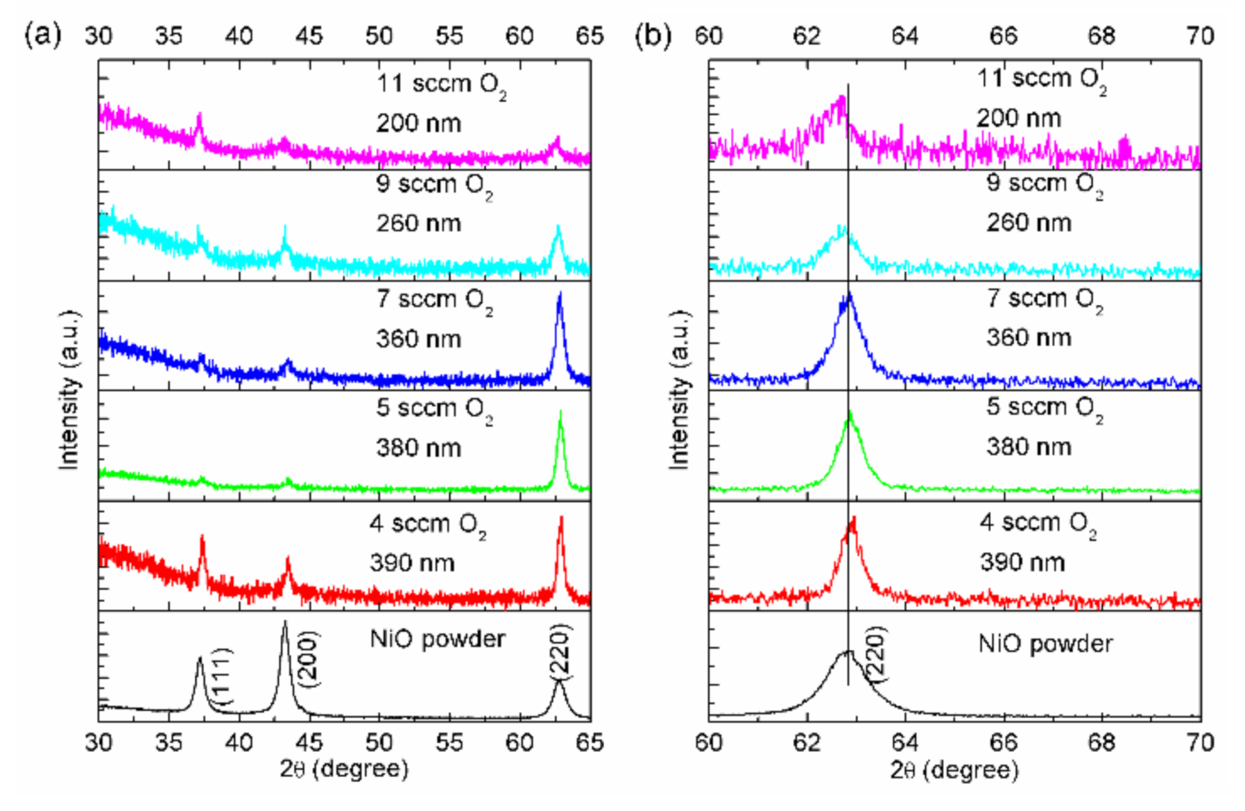
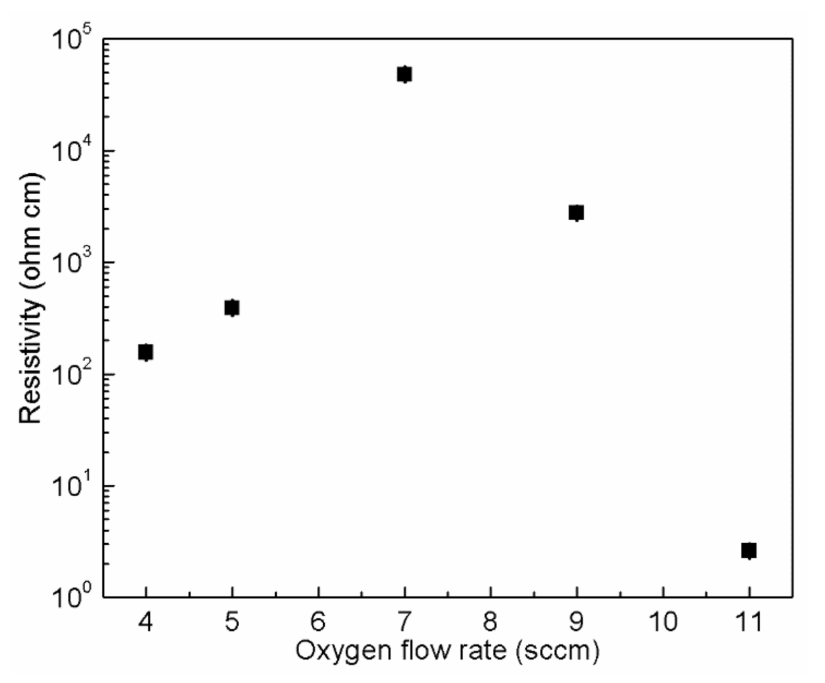
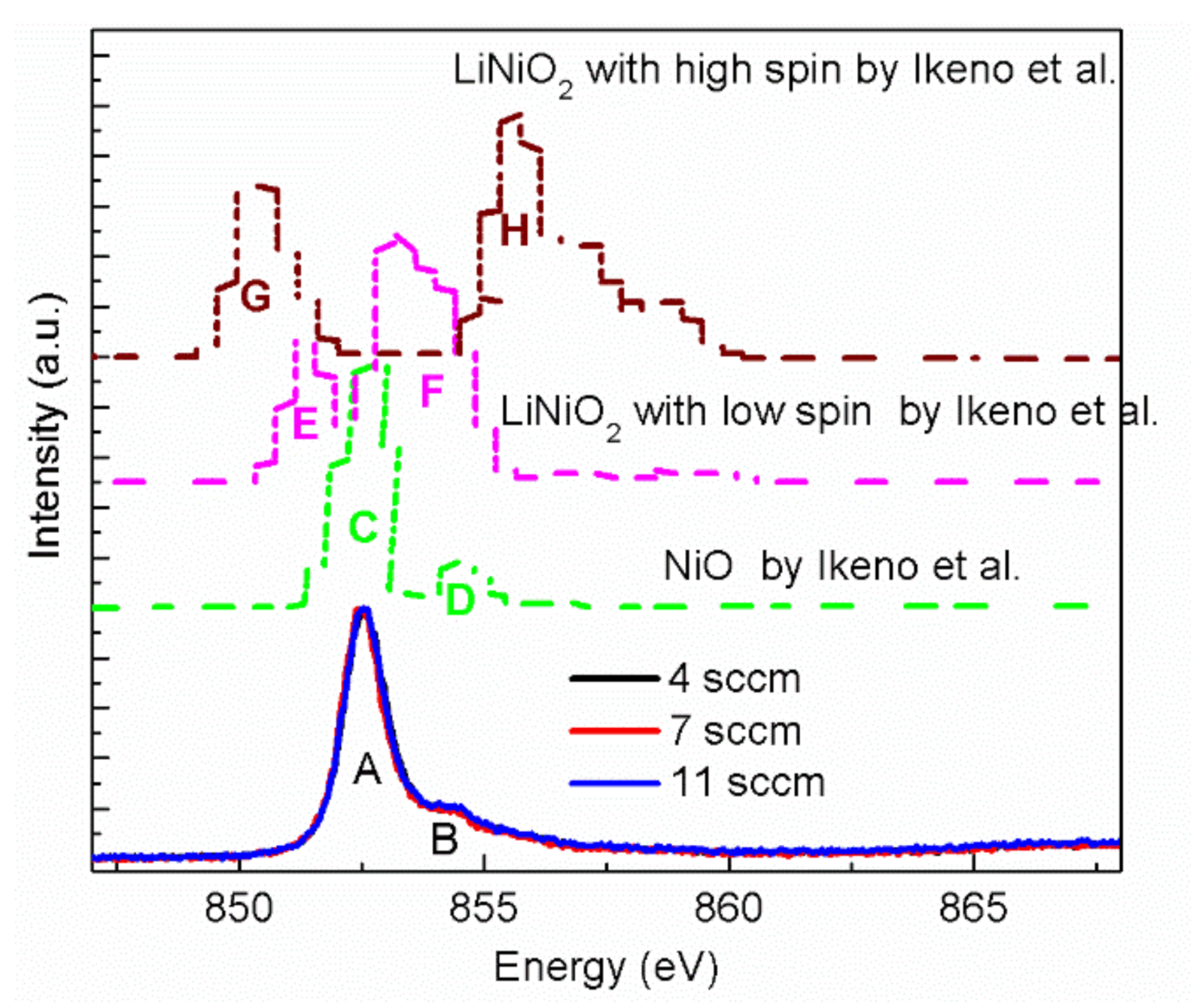
3.1. Oxygen Stoichiometry Dependence of Electrical Properties

X-ray diffractograms of NiO thin films on glass substrates with fixed deposition time (6 min) at various oxygen flow rates, as well as the diffractogram of NiO powder as a reference, are shown in Figure 1. No metallic nickel was evidenced by XRD, implying that all the NiO thin films were single-phase, as seen in Figure 1a. NiO thin films grown with the oxygen flow rates of 4–7 sccm seemed to exhibit the <110> preferred orientation (see Figure 1a). However, such preferred growth disappeared gradually at higher oxygen flow rates, which may have resulted from reductions in the kinetic energy of the sputtered atoms and/or enhancements of oxygen ion bombardment. The magnified (220) diffraction peaks of NiO thin films and powder are shown in Figure 1b. Gradual shifts towards lower angle values with increasing oxygen flow rates are observed in Figure 1b. The desired NiO powder was synthesized in air at very high temperature; therefore, such equilibrium conditions could produce the almost-perfectly stoichiometric NiO with a lattice constant of 0.41976 nm. Without considering the internal stress effect on the diffraction peak positions of thin films, the lattice constants of NiO thin films increased from 0.41944 nm (4 sccm O2) to 0.41950 nm (5 sccm O2), 0.41971 nm (7 sccm O2), 0.42012 nm (9 sccm O2), and 0.42040 nm (11 sccm O2). Thus, increasing the oxygen flow rate seemed to yield a larger crystal constant. In addition, the coherent scattering lengths of these NiO thin films have been evaluated from the full width at half maximum (FWHM) of (220) diffraction peaks using the Scherrer formula. Increasing the oxygen flow rate, the coherent scattering lengths decreased incrementally from 21.03 nm (4 sccm O2) to 18.76 nm (5 sccm O2), 16.29 nm (7 sccm O2), 14.49 nm (9 sccm O2) and 13.94 nm (11 sccm O2). This indicates that larger oxygen flow rates tend to reduce the coherent scattering length of NiO thin films.
In previous studies, we have shown that the phase structure, preferred orientation, and microstructure of thin films are independent of glass or Si (100) substrates, because the amorphous SiO2 layer on single-crystal Si (100) substrate was not removed [29,30,31]. Thus, the microstructures of NiO thin films grown on Si (100) substrates with various oxygen flow rates (4, 7 and 11 sccm) have been studied by TEM. Here, the bright field TEM image and its corresponding electron diffraction pattern of NiO thin film deposited at 11 sccm O2 is presented in Figure 2. The TEM image demonstrates the columnar microstructure, while the diffraction pattern confirms the single cubic phase structure.
The electrical properties of NiO thin films have been investigated. Figure 3 shows the room temperature resistivity of NiO thin films deposited on glass substrates with various oxygen flow rates (4, 5, 7, 9 and 11 sccm). It was seen that the resistivity of NiO thin films strongly depends on the oxygen flow rate. Increasing the oxygen flow rate from 4 to 7 sccm, the average resistivity increased from 155 to 47,724 Ω cm. Continuing to increase the oxygen flow rate to 11 sccm, the resistivity reduced to 2.6 Ω cm. Once the oxygen flow rate exceeded 11 sccm, the deposition rate was extremely low. In addition, Seebeck coefficients of NiO thin films grown with 4, 7 and 11 sccm O2 have also been checked. In the case of thin films deposited with 4 and 11 sccm O2, the Seebeck coefficients were 334 and 277 V/K, indicating their p-type conduction. However, the Seebeck coefficient of NiO thin film grown with 7 sccm O2 could not be determined precisely, probably due to its relatively high resistance.
In order to study the mechanism behind the dependence of oxygen flow rate on resistivity, the compositions of NiO thin films deposited with 4, 7 and 11 sccm O2 were determined by XPS, as shown in Table 1 (see the Supplementary Material for the details of XPS analyses). It is seen that the oxygen contents identified by XPS increased continuously when raising the oxygen flow rate. Low oxygen flow rates, such as at 4 sccm, produced the oxygen sub-stoichiometric NiO thin films. However, higher oxygen flow rates (e.g., 11 sccm) yielded the oxygen over-stoichiometric NiO thin films. Intermediate oxygen flow rates, such as 7 sccm, are susceptible to form stoichiometry much closer to the perfect structure. Although the chemical composition of NiO1.02 attained in NiO thin film grown with 7 sccm was slight oxygen over-stoichiometry, this was the closest to perfect stoichiometry. Such a tendency is also in accordance with the hysteresis effect which occurred in this reactive sputtering process (see Figure S1 in the supplementary information). In addition, the composition of the NiO thin film grown with the oxygen flow rate of 11 sccm was also checked by Rutherford backscattering spectrometry (RBS) at Helmholtz-Zentrum Dresden-Rossendorf, which gave the stoichiometry of NiO1.13 (see Figures S2 and S3 in the supplementary information). Such a composition from RBS was close to that from XPS. Therefore, it is believed that the resistivity of NiO can be tuned by the stoichiometry. Oxygen off-stoichiometry, especially oxygen over-stoichiometry, gives rise to lower resistivity. In contrast, NiO thin films with stoichiometry close to perfect possess relatively high resistivity.
Furthermore, energy loss near edge structure (ELNES) spectra of NiO thin films with discrepant resistivity and compositions have been studied. Figure 4 shows the ELNES spectra of Ni L3 edges attained from our NiO thin films grown with 4, 7 and 11 sccm O2, as well as the theoretical spectra of NiO and LiNiO2 calculated by Ikeno et al. [32]. Examining the experimental spectra in Figure 4, two peaks are clearly visible in the Ni L3 ELNES, labeled as A (852.5 eV) and B (854.4 eV). Traditional hypotheses assume that peak B would correspond to Ni3+ species, and the change in resistivity is explained by the variation of relative integral intensity between peak A and B [22,33,34]. Referring to this hypothesis, NiO thin films with low resistivity (4 or 11 sccm oxygen flow rate) in this work should possess much more Ni3+. Thus, a stronger intensity of peak B is expected. However, such an assumption is contrary to our experimental results. As seen in Figure 4, Ni L3 ELNES spectra of NiO thin films with different resistivity exhibit almost the same features, which seems to indicate that the multipeaks in Ni L3 are the intrinsic characters. This agrees well with the report by Peck et al., that a small change exists in the XAS spectra of bulk and nanoscaled NiO prepared by different methods [35]. Similarly, the Ni 2p3/2 XPS spectra of these thin films also exhibited little difference with each other (see Figure S4 in the supplementary information).
In addition, our experimental Ni L3 ELNES spectra were compared with the reported computational spectra of NiO and LiNiO2 (Ni is in the form of Ni3+ with low or high spin states) calculated by multielectron wave functions [32], as shown in Figure 4. A side-by-side comparison between our experimental and the theoretical spectra of NiO shows a consistent picture (see Figure 4), because the relative intensities and positions of peak C and D mimic the experimental peaks of A and B well. This confirms that peak B in our experimental spectra is the inherent character of NiO, rather than the existence of Ni3+. In contrast, the calculated Ni L3 ELNES spectra of Ni3+ with low or high spin states in LiNiO2 exhibited much more discrepancy than the experimental spectrum of NiO. As shown in Figure 4, the first predominant peaks (E and G) of Ni3+ with low and high spin states are shifted to low-energy losses of 851.9 and 853.6 eV, respectively. However, no significant shift was observed in peak A in our experimental spectra, which also demonstrates the non-existence of Ni3+ in our NiO thin films, Moreover, the ELNES spectra of the O K edge of NiO thin films with tunable resistivity were investigated. Similarly to the Ni L3 ELNES spectra, few differences were observed in the O K edges of NiO thin films (see Figure S5 in the supplementary information).
The non-existence of Ni3+ in NiO thin films evidenced by our ELNES spectra makes the traditional assumptions on tuning the electrical properties of NiO by Ni3+ doubtful. Indeed, the theoretical defect mechanism of NiO does not imply the existence of Ni3+ either [36]. The point defect calculations show that Ni vacancies with negative charges are the predominant defects in non-stoichiometric NiO due to their low formation energy, which produces holes for p-type conduction [36]. Moreover, the formation energy of Ni vacancies in O-rich conditions is much lower than that in O-poor conditions, indicating that there may be a higher density of hole carriers in O-rich conditions [36]. Thus, the resistivity of NiO as a function of oxygen flow rate (or oxygen stoichiometry) (see Figure 3 and Table 1) can be qualitatively understood from the theoretical defect mechanism; NiO thin films grown with an intermediate oxygen flow rate of 7 sccm possess stoichiometry close to perfect. Consequently, the density of Ni vacancies is low, giving rise to high resistivity. In contrast, low oxygen flow rates (such as 4 sccm) and high oxygen flow rates (such as 11 sccm) are O-poor and O-rich conditions, respectively, which could introduce more Ni vacancies. Especially for the oxygen over-stoichiometric NiO thin films grown at high oxygen flow rates (11 sccm), the much lower formation energy of Ni vacancies will produce more hole carriers, yielding smaller resistivity. Here, it is worth noting that the roles of O defects cannot be neglected. For instance, the theoretical calculations show that O vacancies with positive or neutral charges have the lowest formation energy in O-poor conditions (even lower than Ni vacancies) [36]. Thus, certain amounts of O vacancies also exist in NiO thin films with oxygen-poor composition, but they do not generate hole carriers. The dominant source of hole carriers in oxygen-poor compositions is still Ni vacancy.

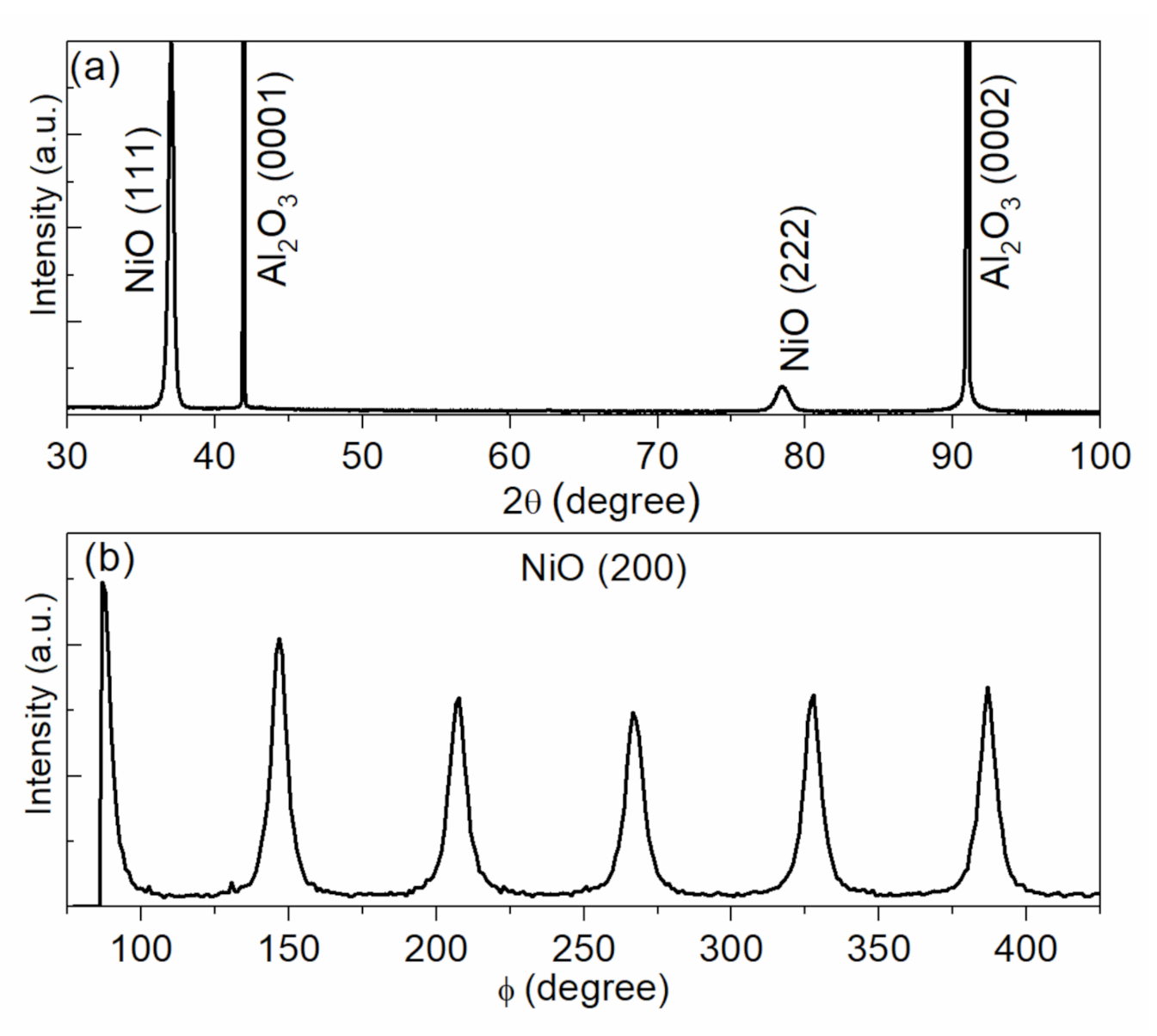
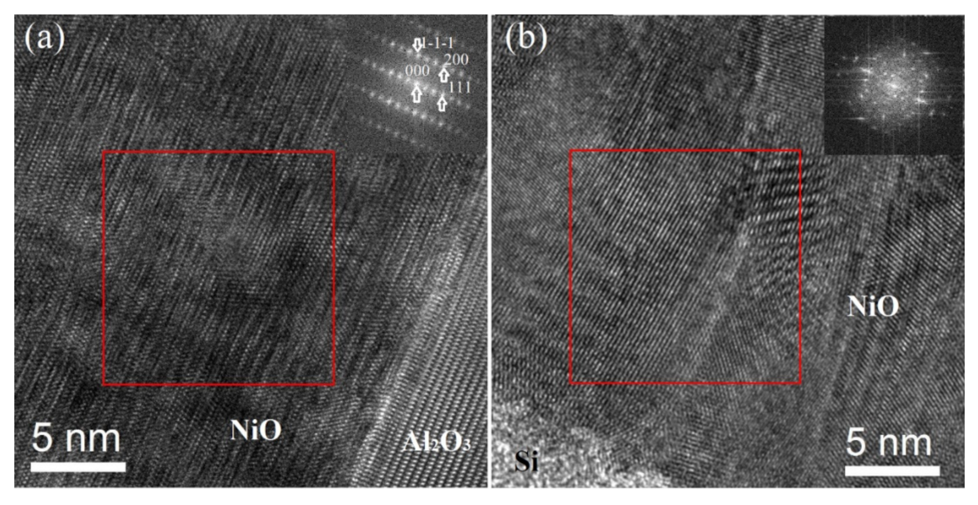
3.2. Microstructure Dependence of Electrical Properties

As discussed before, the 11 sccm oxygen flow rate produced the lowest resistivity of NiO thin films with oxygen over-stoichiometry on non-matched glass substrates. Thus, the same deposition conditions are used to grow NiO thin films on Al2O3 (0001) substrates. Figure 5a shows the θ–2θ scan diffractogram of NiO thin films on Al2O3 (0001). Intensive {111} diffraction peaks of NiO are clearly detected, indicating the high <111> orientation along the c-axis. Additionally, ϕ-scan diffractogram of the (200) (ψ = 54.7) plane shows six peaks with intervals of 60° (see Figure 5b), which indicates the epitaxial growth of NiO thin films [37]. Epitaxial NiO thin films exhibit much stronger diffraction intensity and smaller full width at half maximum (FWHM) values than those on non-matched glass or Si substrates (see Figure 1), even though they are deposited at the same time. This demonstrates better crystallization in epitaxial thin films, which agrees well with the microstructure analyses by high-resolution TEM (HRTEM). As seen in Figure 6a, the uniform crystal orientation, the sharp interface between film and substrate, as well as the fine spots of the fast Fourier transform (FFT) pattern (see the inset of Figure 6a) demonstrate the good crystallization of these epitaxial thin films. In contrast, the HRTEM image of polycrystalline NiO thin films on Si substrate shows the smaller grains with various orientations and a high density of structural defects (such as grain boundaries). Moreover, the FFT pattern of such a polycrystalline thin film does not exhibit the fine spots, indicating some kind of disorder (see the inset of Figure 6b).
The electrical properties of epitaxial NiO thin films have also been studied. Surprisingly, the room temperature resistivity of epitaxial thin film is about 16 Ω cm, which is almost six times larger than that of film on non-matched glass or Si substrates (2.6 Ω cm). These thin films were deposited simultaneously; therefore, their stoichiometries were expected to be close. Thus, the oxygen stoichiometry was not responsible for such different resistivity. Due to significant discrepancy in the microstructure, it is believed that the electrical properties of NiO thin films may also depend on the microstructure. According to the electrical transport mechanism of NiO investigated by Bosman et al. [38], it is shown that NiO possesses almost small polaron characteristics, where a Ni vacancy and the lattice distortion induced by this vacancy can be regarded as a polaron. Typically, in small-polaron transport materials the carrier is slow; it can be imagined that it becomes self-trapped in its own polarization field generated in the lattice, and thus to become localized at a certain site. Moreover, the lattice distortion in small polarons extends to smaller than the lattice constant, yielding a small interaction range for this localized carrier [38]. Therefore, there are much more perfectly periodic lattices between two polarons in epitaxial NiO thin films with less density of structural defects (such as grain boundaries and dislocations), which will reduce the probability of hopping conduction, giving rise to higher resistivity. In contrast, a larger density of structural defects in polycrystalline NiO thin films will facilitate the small polaron transport by reducing the distance between two polarons, giving rise to enhanced conductivity.

4. Conclusions

NiO thin films have been deposited on various substrates (such as glass, Si (100) and Al2O3 (0001)) at room temperature by reactive magnetron sputtering from a metallic Ni target. The electrical properties of NiO thin films have been investigated, revealing the notable dependence of resistivity on oxygen stoichiometry and microstructure. NiO thin films with nearly perfect stoichiometry possess extremely high resistivity, whereas off-stoichiometry induces much lower resistivity, especially for oxygen rich-compositions. ELNES spectra of the Ni L3 edge in these NiO thin films with different resistivity were compared with reported theoretical spectra of NiO and LiNiO2, which ruled out the existence of Ni3+ in NiO thin films. Epitaxial NiO thin films on Al2O3 (0001) substrates exhibited much higher resistivity than films on non-matched glass substrates, demonstrating the influence of microstructure on electrical properties. In epitaxial NiO thin films with a reduced density of structural defects, there were much more perfectly periodic lattices between two polarons, which may reduce the probability of hopping conduction, yielding the higher resistivity.

Supplementary Materials

The following are available online at https://www.mdpi.com/article/10.3390/coatings11060697/s1, Figure S1: Evolution of the oxygen partial pressure as a function of the oxygen flow rate, Figure S2: O1s XPS spectra of various NiO thin films deposited with different oxygen flow rates, Figure S3: RBS spectra of NiO thin film grown with 11 sccm O2, Figure S4: Ni 2p3/2 XPS spectra of NiO thin films deposited with different oxygen flow rates (4, 7 and 11 sccm O2), Figure S5: O K edge ELNES spectra of various NiO thin films deposited with different oxygen flow rates.

Author Contributions

Y.-H.L. carried out main parts of the experiments and wrote the first version of this paper. Y.W. directed the whole study. X.-Y.L., H.S., B.D., and P.Z. contributed to the analysis and discussion of the results. All authors have read and agreed to the published version of the manuscript.

Funding

Y.W. and H.S. are grateful for funding support from the Open Project of State Key Laboratory of Environment-Friendly Energy Materials (19kfhg14) and the Qilu Young Scholar at Shandong University.

Institutional Review Board Statement

Not applicable.

Informed Consent Statement

Not applicable.

Data Availability Statement

The data presented in this study are available on request from thecorresponding author.

Acknowledgments

Y.W. would like to acknowledge Pascal Boulet (Institut Jean Lamour) for the phi-scan measurement, and Johannes von Borany (Helmholtz-Zentrum Dresden-Rossendorf) for the RBS measurements.

Conflicts of Interest

The authors declare no conflict of interest.

References

  1. Zaanen, J.; Sawatzky, G.A.; Allen, J.W. Band gaps and electronic structure of transition-metal compounds. Phys. Rev. Lett. 1985, 55, 418–421. [Google Scholar] [CrossRef]
  2. Bredow, T.; Gerson, A. Effect of exchange and correlation on bulk properties of MgO, NiO, and CoO. Phys. Rev. B 2000, 61, 5194–5201. [Google Scholar] [CrossRef]
  3. Calandra, M.; Rueff, J.P.; Gougoussis, C.; Ceolin, D.; Gorgoi, M.; Benedetti, S.; Torelli, P.; Shukla, A.; Chandesris, D.; Brouder, C. K-edge x-ray absorption spectra in transition-metal oxides beyond the single-particle approximation: Shake-up many-body effects. Phys. Rev. B 2012, 86, 165102. [Google Scholar] [CrossRef] [Green Version]
  4. Taguchi, M.; Matsunami, M.; Ishida, Y.; Eguchi, R.; Chainani, A.; Takata, Y.; Yabashi, M.; Tamasaku, K.; Nishino, Y.; Ishikawa, T.; et al. Revisiting the valence-band and core-level photoemission spectra of NiO. Phys. Rev. Lett. 2008, 100, 206401. [Google Scholar] [CrossRef] [PubMed] [Green Version]
  5. Dutta, T.; Gupta, P.; Gupta, A.; Narayan, J. Effect of Li doping in NiO thin films on its transparent and conducting properties and its application in heteroepitaxial p-n junctions. J. Appl. Phys. 2010, 108, 083715. [Google Scholar] [CrossRef]
  6. Patel, M.; Kim, H.S.; Kim, J. All transparent metal oxide ultraviolet photodetector. Adv. Electron. Mater. 2015, 1, 1500232. [Google Scholar] [CrossRef]
  7. Wang, Y.B.; Wei, X.H.; Chang, L.; Xu, D.G.; Dai, B.; Pierson, J.F.; Wang, Y. Room temperature fabrication of transparent p-NiO/n-ZnO junctions with tunable electrical properties. Vacuum 2018, 149, 331–335. [Google Scholar] [CrossRef]
  8. Castro-Hurtado, I.; Malagù, C.; Morandi, S.; Pérez, N.; Mandayo, G.G.; Castaño, E. Properties of NiO sputtered thin films and modeling of their sensing mechanism under formaldehyde atmospheres. Acta Mater. 2013, 61, 1146–1153. [Google Scholar] [CrossRef]
  9. Mihelcic, M.; Surca Vuk, A.; Jerman, I.; Orel, B.; Svegl, F.; Moulki, H.; Faure, C.; Campet, G.; Rougier, A. Comparison of electrochromic properties of Ni1−xO in lithium and lithium-free aprotic electrolytes: From Ni1−xO pigment coatings to flexible electrochromic devices. Sol. Energy Mater. Sol. Cells 2014, 120, 116–130. [Google Scholar] [CrossRef]
  10. Moulki, H.; Park, D.H.; Min, B.K.; Kwon, H.; Hwang, S.J.; Choy, J.H.; Toupance, T.; Campet, G.; Rougier, A. Improved electrochromic performances of NiO based thin films by lithium addition: From single layers to devices. Electrochim. Acta 2012, 74, 46–52. [Google Scholar] [CrossRef]
  11. Ratcliff, E.L.; Meyer, J.; Steirer, K.X.; Garcia, A.; Berry, J.J.; Ginley, D.S.; Olson, D.C.; Kahn, A.; Armstrong, N.R. Evidence for near-surface NiOOH species in solution-rocessed NiO. Chem. Mater. 2011, 23, 4988–5000. [Google Scholar] [CrossRef]
  12. Chen, W.; Wu, Y.; Yue, Y.; Liu, J.; Zhang, W.; Yang, X.; Chen, H.; Bi, E.; Ashraful, I.; Gratzel, M.; et al. Efficient and stable large-area perovskite solar cells with inorganic charge extraction layers. Science 2015, 350, 944–948. [Google Scholar] [CrossRef] [Green Version]
  13. Kuneš, J.; Anisimov, V.I.; Skornyakov, S.L.; Lukoyanov, A.V.; Vollhardt, D. NiO: Correlated band structure of a charge-transfer insulator. Phys. Rev. Lett. 2007, 99, 156404. [Google Scholar] [CrossRef] [PubMed] [Green Version]
  14. Wrobel, F.; Park, H.; Sohn, C.; Hsiao, H.W.; Zuo, J.M.; Shin, H.; Lee, H.N.; Ganesh, P.; Benali, A.; Kent, P.R.C.; et al. Doped NiO: The mottness of a charge transfer insulator. Phys. Rev. B 2020, 101, 195128. [Google Scholar] [CrossRef]
  15. Gupta, P.; Dutta, T.; Mal, S.; Narayan, J. Controlled p-type to n-type conductivity transformation in NiO thin films by ultraviolet-laser irradiation. J. Appl. Phys. 2012, 111. [Google Scholar] [CrossRef]
  16. Thimsen, E.; Martinson, A.B.F.; Elam, W.; Pellin, M.J. Energy levels, electronic properties, and rectification in ultrathin p-NiO films synthesized by atomic layer deposition. J. Phys. Chem. C 2012, 116, 16830–16840. [Google Scholar] [CrossRef]
  17. Irwin, M.D.; Servaites, J.D.; Buchholz, D.B.; Leever, B.J.; Liu, J.; Emery, J.D.; Zhang, M.; Song, J.H.; Durstock, M.F.; Freeman, A.J.; et al. Structural and electrical functionality of NiO interfacial films in bulk heterojunction organic solar cells. Chem. Mater. 2011, 23, 2218–2226. [Google Scholar] [CrossRef]
  18. Soo Kim, D.; Chul Lee, H. Nickel vacancy behavior in the electrical conductance of nonstoichiometric nickel oxide film. J. Appl. Phys. 2012, 112, 034504. [Google Scholar] [CrossRef]
  19. Chen, H.; Harding, J.H. Nature of the hole states in Li-doped NiO. Phys. Rev. B 2012, 85, 115127. [Google Scholar] [CrossRef] [Green Version]
  20. Jang, W.L.; Lu, Y.M.; Hwang, W.S.; Hsiung, T.L.; Wang, H.P. Point defects in sputtered NiO films. Appl. Phys. Lett. 2009, 94, 062103. [Google Scholar] [CrossRef]
  21. Molaei, R.; Bayati, R.; Narayan, J. Crystallographic characteristics and p-type to n-type transition in epitaxial NiO thin film. Cryst. Growth Des. 2013, 13, 5459–5465. [Google Scholar] [CrossRef]
  22. Cho, D.-Y.; Song, S.J.; Kim, U.K.; Kim, K.M.; Lee, H.-K.; Hwang, C.S. Spectroscopic investigation of the hole states in Ni-deficient NiO films. J. Mater. Chem. C 2013, 1, 4334. [Google Scholar] [CrossRef]
  23. Soriano, L.; Preda, I.; Gutiérrez, A.; Palacín, S.; Abbate, M.; Vollmer, A. Surface effects in the Ni 2p X-ray photoemission spectra of NiO. Phys. Rev. B 2007, 75, 233417. [Google Scholar] [CrossRef] [Green Version]
  24. Josefsson, I.; Kunnus, K.; Schreck, S.; Fo, A.; De Groot, F.; Wernet, P.; Odelius, M. Ab initio calculations of X-ray spectra: Atomic multiplet and molecular orbital effects in a multiconfigurational SCF approach to the L-edge spectra of transition metal complexes. J. Phys. Chem. Lett. 2012, 3, 3565–3570. [Google Scholar] [CrossRef] [Green Version]
  25. Haverkort, M.W.; Zwierzycki, M.; Andersen, O.K. Multiplet ligand-field theory using Wannier orbitals. Phys. Rev. B 2012, 85, 165113. [Google Scholar] [CrossRef] [Green Version]
  26. Wang, Y.; Ghanbaja, J.; Bruyère, S.; Boulet, P.; Soldera, F.; Horwat, D.; Mücklich, F. Local heteroepitaxial growth to promote the selective growth orientation, crystallization and interband transition of sputtered NiO thin films. CrystEngComm 2016, 18, 1732–1739. [Google Scholar] [CrossRef]
  27. Greczynski, G.; Hultman, L. X-ray photoelectron spectroscopy: Towards reliable binding energy referencing. Prog. Mater. Sci. 2020, 107, 100591. [Google Scholar] [CrossRef]
  28. Wang, Y.; Lany, S.; Ghanbaja, J.; Fagot-Revurat, Y.; Chen, Y.P.; Soldera, F.; Horwat, D.; Mücklich, F.; Pierson, J.F. Electronic structures of Cu2O, Cu4O3 and CuO: A joint experimental and theoretical study. Phys. Rev. B 2016, 94, 245418. [Google Scholar] [CrossRef] [Green Version]
  29. Wang, Y.; Ghanbaja, J.; Soldera, F.; Migot, S.; Boulet, P.; Horwat, D.; Mücklich, F.; Pierson, J.F. Tuning the structure and preferred orientation in reactively sputtered copper oxide thin films. Appl. Surf. Sci. 2015, 335, 85–91. [Google Scholar] [CrossRef]
  30. Wang, Y.; Ghanbaja, J.; Soldera, F.; Boulet, P.; Horwat, D.; Mücklich, F.; Pierson, J.F. Controlling the preferred orientation in sputter-deposited Cu2O thin films: Influence of the initial growth stage and homoepitaxial growth mechanism. Acta Mater. 2014, 76, 207–212. [Google Scholar] [CrossRef]
  31. Wang, Y.; Ghanbaja, J.; Soldera, F.; Boulet, P.; Horwat, D.; Mücklich, F.; Pierson, J.F. Local homoepitaxial growth in sputtered NiO thin films: An effective approach to tune the crystallization, preferred growth orientation, and electrical properties. Phys. Status Solidi Rapid Res. Lett. 2018, 12, 1800191. [Google Scholar] [CrossRef]
  32. Ikeno, H.; Tanaka, I.; Koyama, Y.; Mizoguchi, T.; Ogasawara, K. First-principles multielectron calculations of Ni L2,3 NEXAFS and ELNES for LiNiO2 and related compounds. Phys. Rev. B 2005, 72, 075123. [Google Scholar] [CrossRef]
  33. Lin, F.; Nordlund, D.; Weng, T.; Moore, R.G.; Gillaspie, D.T.; Dillon, A.C.; Richards, R.M.; Engtrakul, C. Hole doping in Al-containing nickel oxide materials toimprove electrochromic performance. ACS Appl. Mater. Interfaces 2013, 5, 301–309. [Google Scholar] [CrossRef] [PubMed]
  34. Peng, H.Y.; Li, Y.F.; Lin, W.N.; Wang, Y.Z.; Gao, X.Y.; Wu, T. Deterministic conversion between memory and threshold resistive switching via tuning the strong electron correlation. Sci. Rep. 2012, 2, 442. [Google Scholar] [CrossRef] [PubMed] [Green Version]
  35. Peck, M.A.; Langell, M.A. Comparison of nanoscaled and bulk NiO structural and environmental characteristics by XRD, XAFS, and XPS. Chem. Mater. 2012, 24, 4483–4490. [Google Scholar] [CrossRef]
  36. Lany, S.; Osorio-Guillen, J.; Zunger, A. Origins of the doping asymmetry in oxides: Hole doping in NiO versus electron doping in ZnO. Phys. Rev. B 2007, 75, 241203. [Google Scholar] [CrossRef] [Green Version]
  37. Wang, Y.; Ghanbaja, J.; Boulet, P.; Horwat, D.; Pierson, J.F. Growth, interfacial microstructure and optical properties of NiO thin films with various types of texture. Acta Mater. 2019, 164, 648–653. [Google Scholar] [CrossRef] [Green Version]
  38. Bosman, A.J.; van Daal, H.J. Small-polaron versus band conduction in some transition-metal oxides. Adv. Phys. 1970, 19, 1–117. [Google Scholar] [CrossRef]
Figure 1. (a) θ–2θ scan diffractograms of NiO thin films (200–390 nm) deposited on glass substrates with different oxygen flow rates. The deposition time was fixed at 6 min. The diffractogram of NiO powder is plotted at the bottom as a reference. (b) Magnified (220) diffraction peaks of NiO.
Coatings 11 00697 g001
Figure 2. Bright field TEM image (a) and the electron diffraction pattern (b) of NiO thin films deposited with 11 sccm O2 on Si (100) substrates.
Coatings 11 00697 g002
Figure 3. Room temperature resistivity of NiO thin films deposited on glass substrates with different oxygen flow rates.
Coatings 11 00697 g003
Figure 4. Ni L3 edge ELNES spectra of NiO thin films with different oxygen flow rates. The theoretical spectra of NiO and LiNiO2 calculated by Ikeno et al. [32] are presented for comparison. The intensity has been normalized by the height.
Coatings 11 00697 g004
Figure 5. (a) θ–2θ scan diffractograms of NiO thin films (about 200 nm thick) deposited on Al2O3 (0001) substrates with 11 sccm oxygen flow; (b) θ–2θ scan diffractogram of the (200) plane.
Coatings 11 00697 g005
Figure 6. HRTEM images of an epitaxial NiO thin film on Al2O3 substrate (a) and polycrystalline thin film on Si substrate (b). These films were deposited at the same time. Insets show the FFT patterns of selected regions marked by red frames.
Coatings 11 00697 g006
Table 1. Resistivity and compositions of NiO thin films.
O2 Flow Rate (sccm) to Grow NiOResistivity (Ω cm)Composition by XPS
4155NiO0.96
747,724NiO1.02
112.6NiO1.12
Publisher’s Note: MDPI stays neutral with regard to jurisdictional claims in published maps and institutional affiliations.

