1. Introduction
Energy production by means of fusion technology is one of the most ambitious projects that mankind initiated in the last century. The world’s largest research facility so far, which is still under construction, is ITER in Cadarache in southern France. Thirty-five nations are collaborating to erect a facility that hopefully proves the feasibility of fusion as a large-scale and carbon-free source of energy [
1]. It is based on the so-called tokamak concept that uses a magnetic confinement to heat, compress and hold the plasma in place. Many other research facilities are operated in parallel by international consortia throughout the world. In Germany this is Wendelstein 7-X (W7-X) in Greifswald (stellarator concept) and ASDEX Upgrade in Garching (tokamak concept). The Joint European Torus (JET) in Oxfordshire in UK is another important European research facility. USA, China, Japan, Korea and India are planning or already running their own research centers. However, besides the magnetic confinement principle (tokamak and stellarator), there exist other fusion concepts like inertial confinement that are being developed in parallel.
Fusion technology involves thousands of components that have to be designed and integrated into an overall functionable system. The core components comprise the vacuum torus vessel and several types of superconducting magnetic coils to heat the plasma and keep it in place. Other important components allow for injection of microwaves for plasma heating, as well as components for plasma diagnostics.
Electron–cyclotron resonance heating (ECRH) is one of the main concepts for variable microwave heating of the plasma. Gyrotrons are the main source for the microwave power and are capable of operating in the radio frequency (RF) range of 100–200 GHz with an output power of 1–2 MW. In the case of ITER, they are operated at a frequency of 170 GHz running at a continuous power of 1 MW. In total, 24 gyrotrons will be installed at ITER in the first phase.
A major step in the development and commissioning phase of gyrotrons is extensive testing and conditioning of the device. Stable and reliable RF loads are required to drive the gyrotron to full performance. We report on an RF load with a cylinder, covered with RF absorbing material as the main element.
The development of absorber coatings used in fusion reactor components began in the last decade of the last century. In order to efficiently work as a microwave absorber in the relevant wave length, ceramic coatings with thickness values in a typical range of 100 to 200 µm are required. Resonant coatings in this thickness range can exceed absorption values of 90% for 140 GHz microwave stray radiation [
2]. The most important requirements of the ceramic materials are a high dielectric constant, a reasonable high heat conductivity, high resistance against electromagnetic and thermal loads and a good substrate adhesion [
2]. Moreover, a high vacuum compatibility is required to minimize outgassing effects induced by the desorption of volatile substances. Nearly all components in fusion reactors that are situated close to the plasma are operated under high or ultrahigh vacuum conditions. Regarding the requested properties and coating thickness range, thermal spraying in general is the technology of choice to apply oxide and some non-oxide coatings. Plasma spraying as the industrial standard, either operated in vacuum (VPS) or under atmospheric conditions (APS), has proven to be a suitable technique to apply ceramic coatings on various metal components (Cu, Mo, Al, Co, carbon, etc.) for this purpose. Most used absorber materials at present are chromium oxide (Cr
2O
3), mixed alumina-titania (Al
2O
3/TiO
2) sprayed using APS and boron carbide (B
4C) sprayed using VPS. Depending of the component, to which the coating is applied, one of these ceramic materials may be favored. For thermally highly loaded devices that are operated close to the plasma ring, an absorber coating with a higher thermal conductivity may be of advantage. As shown in [
3], chromium oxide has some benefits in direct comparison to other oxides like alumina-titania or zirconia based coatings. It also exhibits a higher melting point and can withstand high thermal loads without showing any alterations in its microstructure.
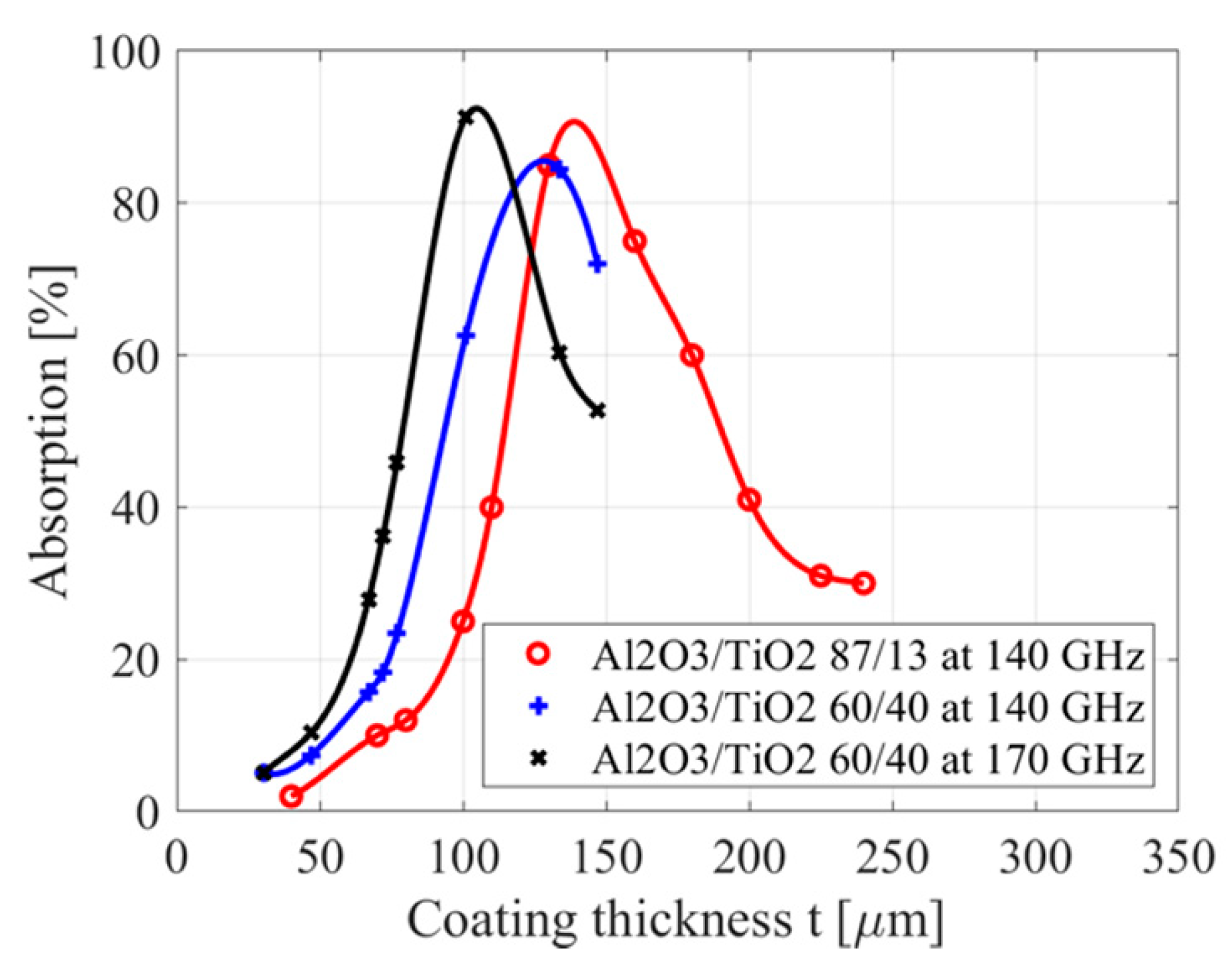
An in depth study of the absorption behavior of different APS sprayed oxides ceramic coatings for 140 GHz stray radiation was worked out in [
4]. The application in mind was the coating of water-cooled baffle shields that protect cryo-pumps and prevent them from heating up in the microwave stray field of the W7-X fusion reactor in Greifswald. For this purpose, an effective absorber coating was searched. Aluminium oxide, chromium oxide, titanium oxide, zirconium oxide and different mixtures of alumina-titania were evaluated and compared. The study revealed that mixed alumina-titania coatings achieved the highest absorption values of over 90%. However, within different ratios (97/3; 87/13; 60/40), different maximum absorption values were observed, with a 50/50 mixture showing the highest values. Moreover, spray angle and grain size distribution of the initial spray powder also had a tremendous effect of the maximum absorption value.
The development of gyrotrons for W7-X as well as ITER has induced some more efforts to develop absorber coatings, especially for testbed dummy loads, as published in [
5]. The paper describes the basic concept for a dummy load design with a mixed aluminum titanium oxide absorption coating. A prototype with a steel tube body was tested successfully. It can be regarded as the technical precursor of the copper tube used in this work. In [
6], plasma sprayed B
4C and Cr
2O
3 as single coatings and mixed bilayer of Cr
2O
3·B
4C were evaluated for high power loads going up to 1 MW/m
2. The paper discusses advantages and drawbacks of the different materials and emphasizes the importance of a high thermal diffusivity which is best for B
4C, acceptable for Cr
2O
3 but somewhat limited for mixed alumina-titania. VPS also shows superior results if directly compared to APS due to the lower porosity of the coatings. Since then, more work has been published for further improvements of high-power dummy load design capable of collecting radiation power pulses in the range 1–2 MW/m
2. Several research groups from Japan [
7,
8] presently working at ITER and JT60SA on this subject. Similar effort is still going on to coat bolometers and other highly loaded devices that are operated close to the plasma ring for diagnostic purposes, as described in [
9] from a research group working at W7-X.
2. Radio Frequency Technical Requirements and Design Principles
The main design goals for the high-power microwave load under consideration can be summarized as follows:
The load should be capable of absorbing at least 1.5 MW of microwave power at frequency levels in the range 140 GHz to 170 GHz.
The back-reflected power from the load has to be as small as possible.
The distribution of the microwave power on the absorbing area of the load should be as homogenous as possible to avoid the formation of thermal hotspots.
The mechanical design of the load should be robust and it has to be easy to cool.
If absorbing coating is applied, both the absorbing material and its connection to the underlying structure should withstand excessive heating and electric arcing events.
The overall costs for components and manufacturing should be in a reasonable frame.
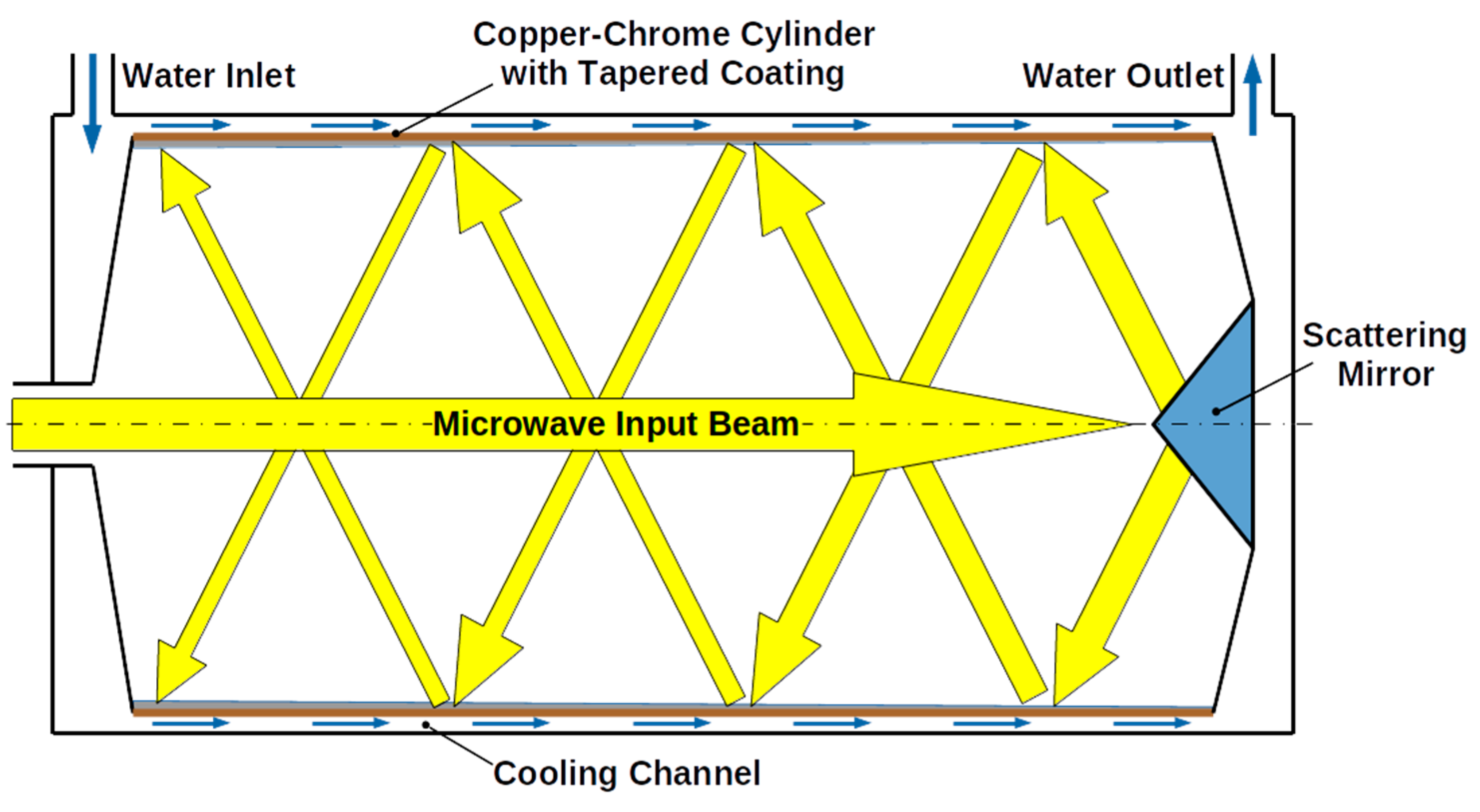
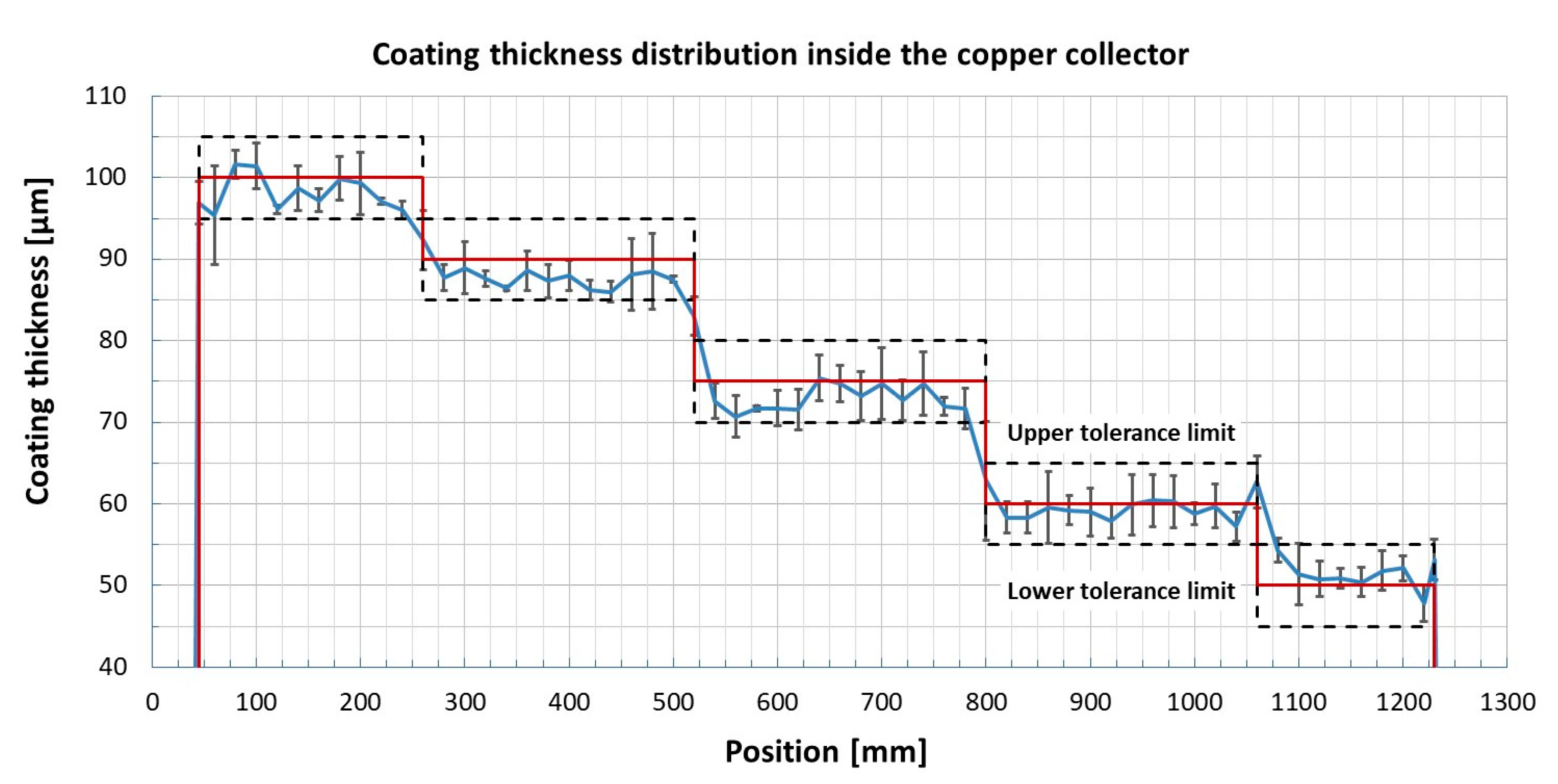
Figure 1 shows the general concept we used for the design of the load: It is based on a symmetric cylindrical structure, where the microwave beam is axially injected through an input port from one side, scattered by a conical mirror on the opposite site and from there distributed to the coated cylindrical surface by multiple reflections. Tapering of the absorbing ceramic layer on the cylinder allows an adaption and balancing of the power density on the structure to avoid hotspots, especially in the case of the first impact of the scattered microwave beam [
5,
10]. This requirement implies that the thickness of the layer increases from the mirror side to the input area according to the decreasing microwave power density. Finally, the required local thickness of the layer is determined by microwave absorption measurements (see
Section 4.3).
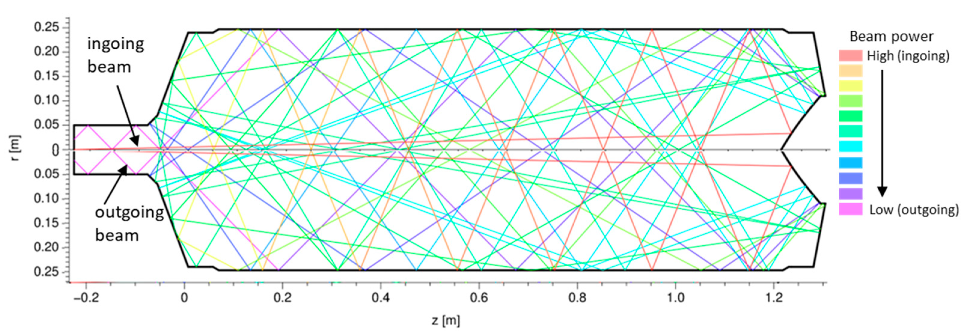
For the design of the load we used a relatively simple “ballistic” ray-tracing code, which even does not take into account the wave diffraction. It simply propagates a larger number of single rays through the geometry, resampling an injected Gaussian beam. At each reflection point, the given power of the ray is reduced according to the assumed absorption coefficient of the respective material until the power of the ray is non-significant or the ray has left the structure through the input port.
Figure 2 exemplarily indicates how such a single ray propagates through the geometry, losing its power after multiple reflections. Beside the power density distribution on the internal walls of the load, the code also gives information about the back-reflected power (by integrating the remaining power of all rays leaving the load through the input port).
While the described simple numerical tool has its limitations, it is sufficient to design and optimize the internal shape of the load, especially the scattering conical mirror. In addition, it allows tuning the variable thickness of the absorbing ceramic layer to avoid excessive values of the power density on the wall, taking into account the measurements of the absorbers described in
Section 4.3.
Figure 3 shows the expected load profile on the cylindrical part in the case of 1.5 MW injected microwave power at a frequency of 140 GHz in the case of the already optimized design. Each incident beam at the input of the load is assigned a certain power, when this beam hits the circumferential surface of the load, the power is reduced by the absorption coefficient defined at this point. Adding up the losses of the rays gives the power per area. Since none of the peaks exceeds 125 W/cm², overheating problems of the thermally well conducting water-cooled copper-chrome structure are not expected [
5]. The calculated back-reflected microwave power leaving the load has a value of 2.4% and is therefore easily manageable.
3. Materials and Methods
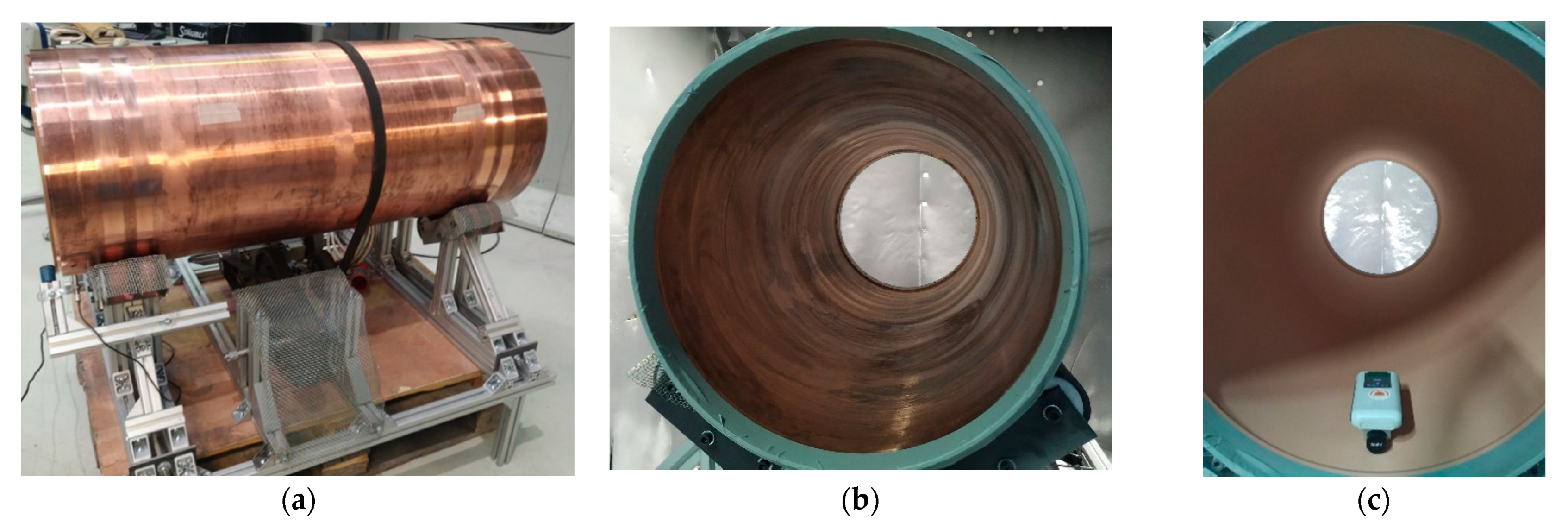
3.1. Copper Collector
The copper collector consists of a tube manufactured by centrifugal casting of a CuCr1-C GZ alloy (DIN 2.1292), with the dimensions summarized in
Table 1. Photographs of the tube during preparation are shown in
Figure 4.
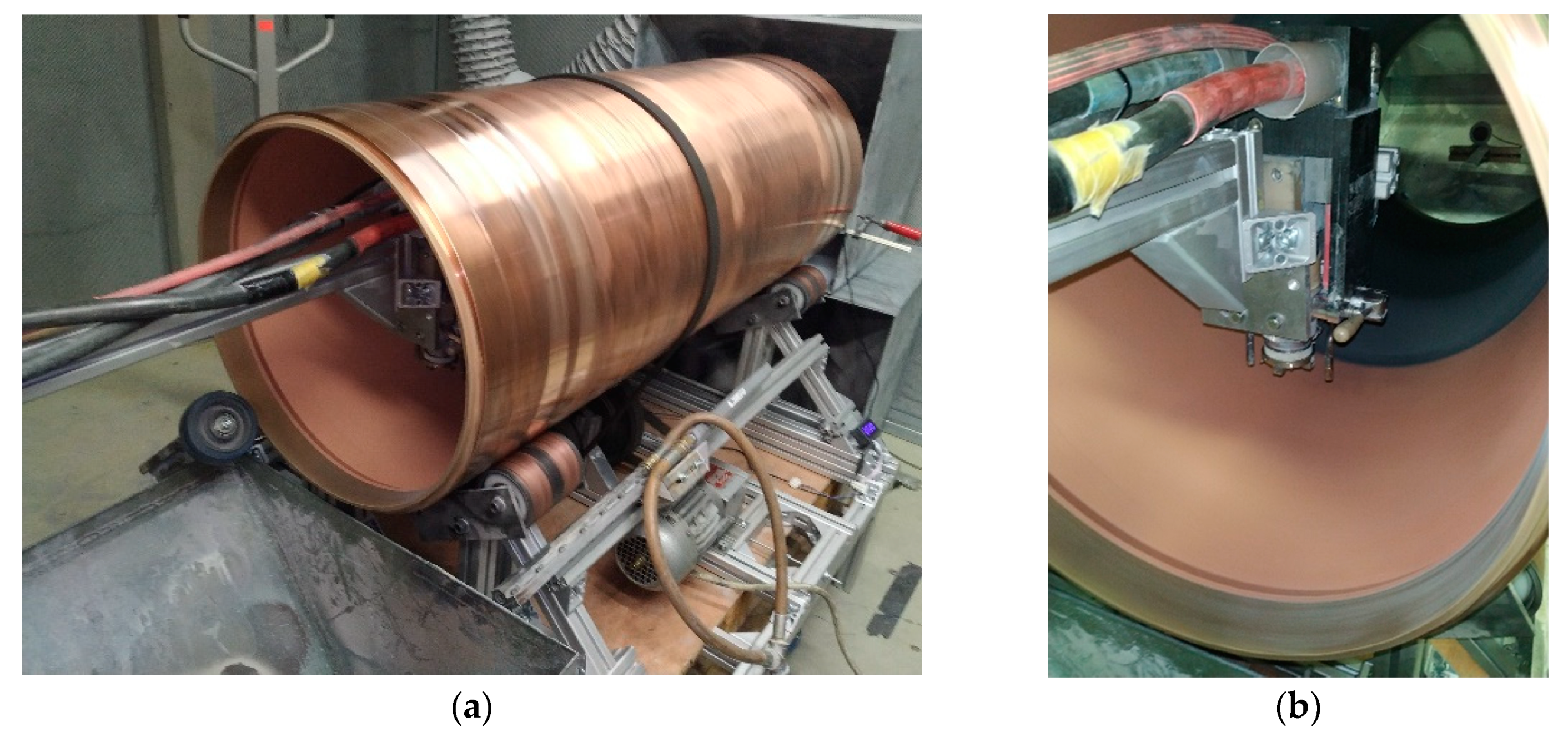
The state-of-the-art for internal coatings of cylinders are miniaturized rotating spray torches, in which part is fixed during the coating process and the cylindrical surface is coated by an axial moving and simultaneously rotating torch [
11]. This technique is especially applicable for coating of small diameter cylinders, such as cylinder liner surfaces in engine blocks with a diameter of typically 90 mm. However, for larger diameters, the rotation of the tubular part with a synchronized linear movement of the torch is more meaningful. In this case, a handling system is used to position the part exactly under rotation with the centerline of the cylindrical surface [
12]. This approach allows for using a standard plasma torch setup operated at optimal spray distance (~150 mm) where the highest particle velocities can be achieved [
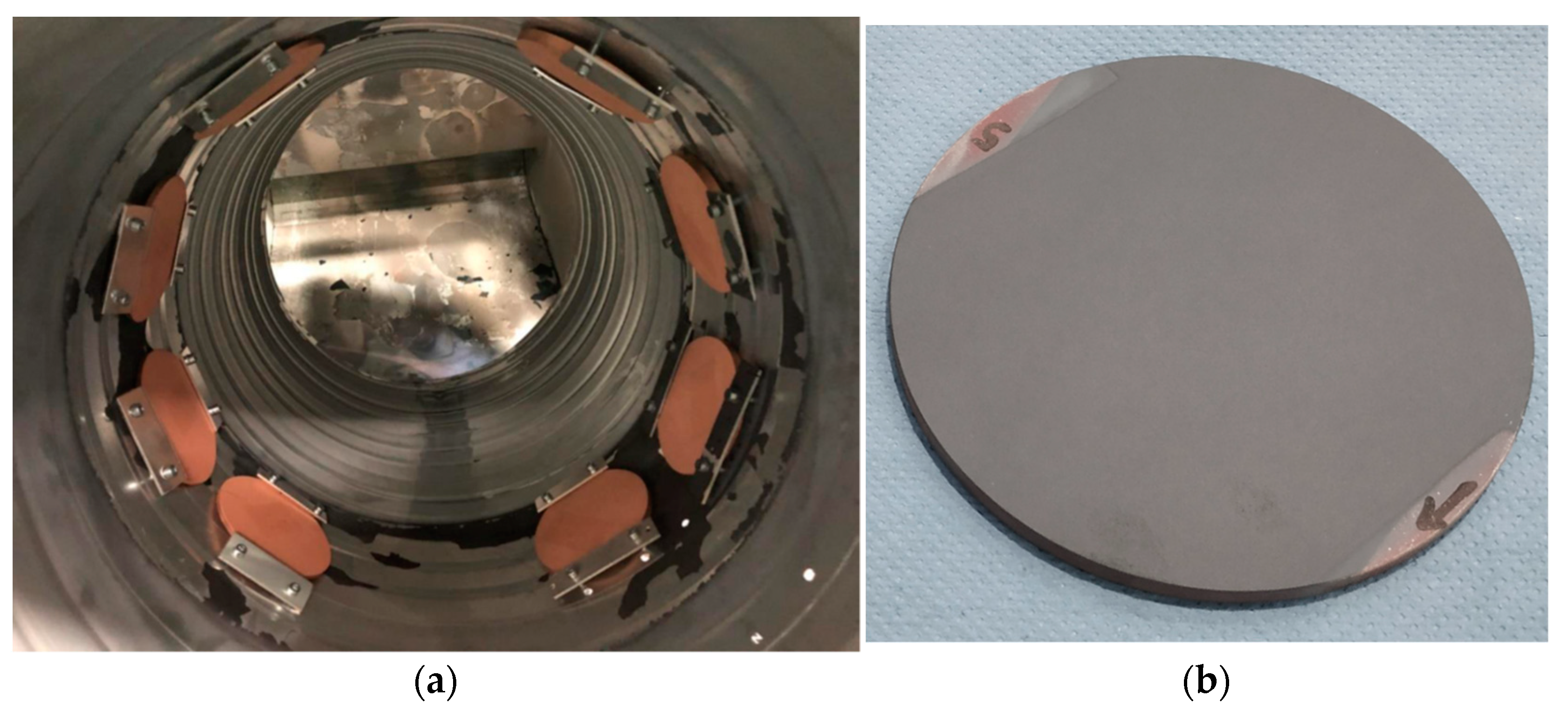
13]. This way, a dense coating microstructure and optimal coating adhesion can be achieved. To rotate the copper collector, a hand-ling system was designed and constructed, transmitting the rotation with a belt drive, as shown in
Figure 5a. The torch is mounted to an extension of the robot system that allows for entering the cylinder and moving in an axial direction synchronously to obtain a 2 mm offset per cylinder revolution, as shown in
Figure 5b.
3.2. Powder Feedstock
In a previous work, different oxide coatings were analyzed, revealing that coating thickness, grain size and material composition strongly influence the system absorption [
4]. It turned out that Al
2O
3 and TiO
2 mixed powders in different compositions led to higher absorption values compared to pure oxide ceramic materials, with an increasing absorption capability with increasing content of TiO
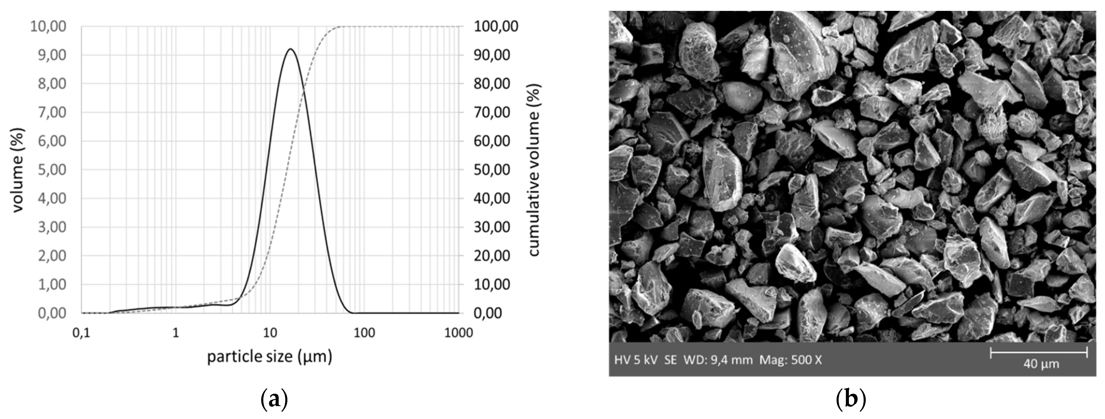
2. All the spray powders had the same particle size distribution of −20 + 5 µm (prevalent mesh size notation based on ASTM B214 sieve analysis, referring to a particle size distribution of D
10 = 5 and D
90 = 20, respectively). The coating thickness was fixed to 150 µm [
4].
The selected spray powder by consideration of previous works is an Al
2O
3/TiO
2 60/40 mixture for APS coatings supplied by Oerlikon Metco AG (Pfäffikon, Switzerland), with the characteristics summarized in
Table 2.
3.3. Coating Deposition and Characterization
Atmospheric plasma spraying was performed using a standard F6 type plasma gun from GTV GmbH (Luckenbach, Germany). The spray torch was guided by a six-axis robot system type RX130B from Stäubli International AG (Pfäffikon, Switzerland). Plasma parameters were adjusted in order to achieve a well adherent and dense coating structure. Powder feed rate was adjusted to achieve a suitable coating thickness in the range of 15 µm per spray pass using a PF962 powder feeder from GTV GmbH (Luckenbach, Germany). The coating thickness per past is adjusted by modifying the amount of powder injected during the process adjusting the rotation speed of the feed disc. The optimized spray parameters that were finally applied for coating operation are summarized in
Table 3.
Surface activation of the inner tube surface has been done by bead blasting with glass beads (300 µm) and degreased using acetone before and after the bead blasting process in order to enhance the mechanical adhesion of the coating to the substrate. The considerably soft material had to be treated carefully to avoid implantation of the bead particles and therefor this operation was performed using a reduced air pressure of 2 bar. A surface roughness with Ra 5.3 µm and Rz 40 µm was achieved. Surface roughness was measured using a contact profilometer type Perthometer Concept from Mahr GmbH (Göttingen, Germany), Rz and Ra values were determined according to DIN EN ISO 4287.
The particle size distribution of the Al2O3/TiO2 60/40 mixture powder was determined by means of laser diffraction particle size analysis in a Mastersizer S from Malvern Panalytical Ltd. (Malvern, United Kingdom) in order to ensure the powder specifications. The material was investigated by scanning electronic microscopy (SEM); the sample was sputter-coated with gold and examined in a LEO VP 438 from Leo Elektronenmikroskopie GmbH (Oberkochen, Germany).
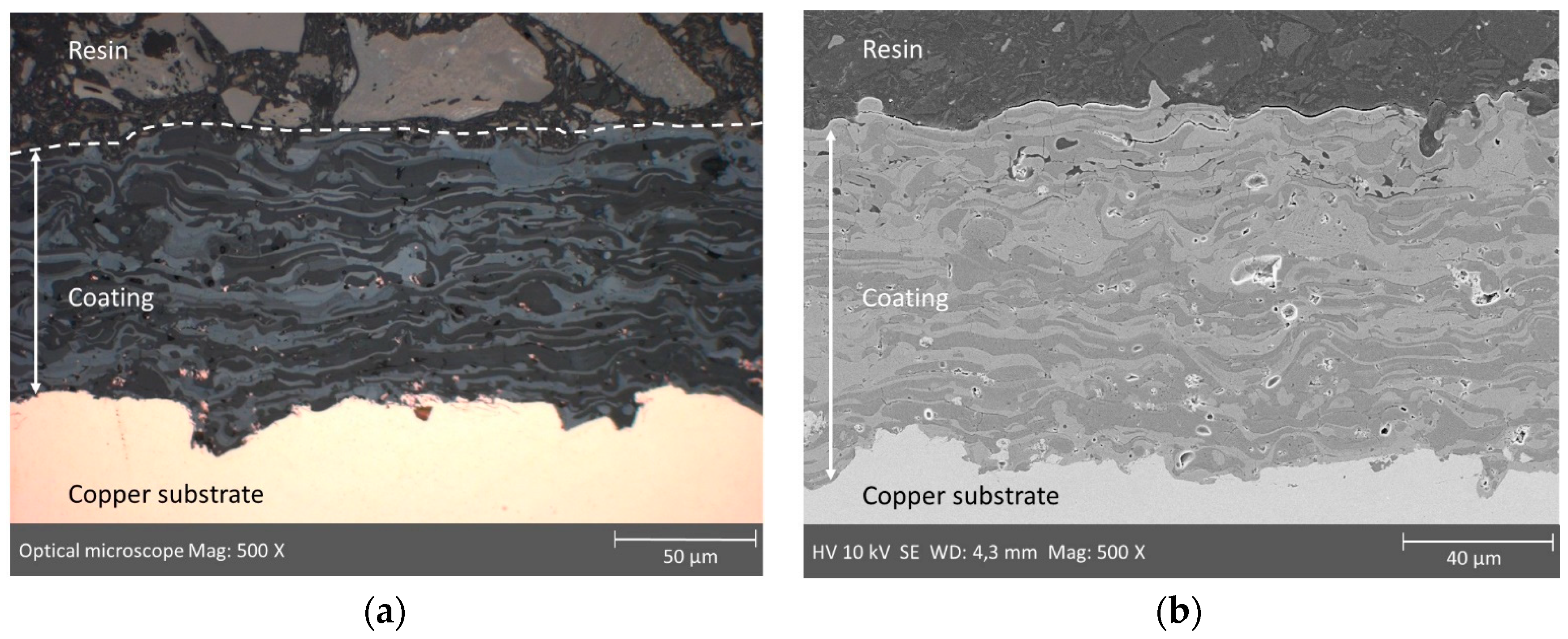
Prior to spraying on the tube component, testing of the spray process was performed on flat samples that were mounted inside a dummy tube with the same diameter to be coated under similar conditions as the absorber coating. This way, a comparable spray process situation like that on the real component is guaranteed. Test samples of CuCrZr copper alloy (formerly CuCrZr), with discs geometry of 124 mm diameter and 8 mm thickness, were coated and used for coating characterization regarding absorption. Coating characterization was done by metallographic cross section preparation and optical micrograph images of the coatings were performed using a Leica MEF4M (Leica GmbH, Wetzlar, Germany) as well as SEM micrographs.
The coating thickness is determined in the copper collector by non-destructible methods, using a portable contact system DUALSCOPE® FMP100 coating thickness gauge from Helmut-Fischer GmbH (Germany), which uses the eddy current testing method (DIN EN ISO 2360) for non-ferrous metals. Temperature measurements during the coating process were performed using an IR pyrometer type Optris CTlaser LTF-SF-CB8 from Micro-Epsilon Messtechnik GmbH & Co. KG. (Ortenburg, Germany).
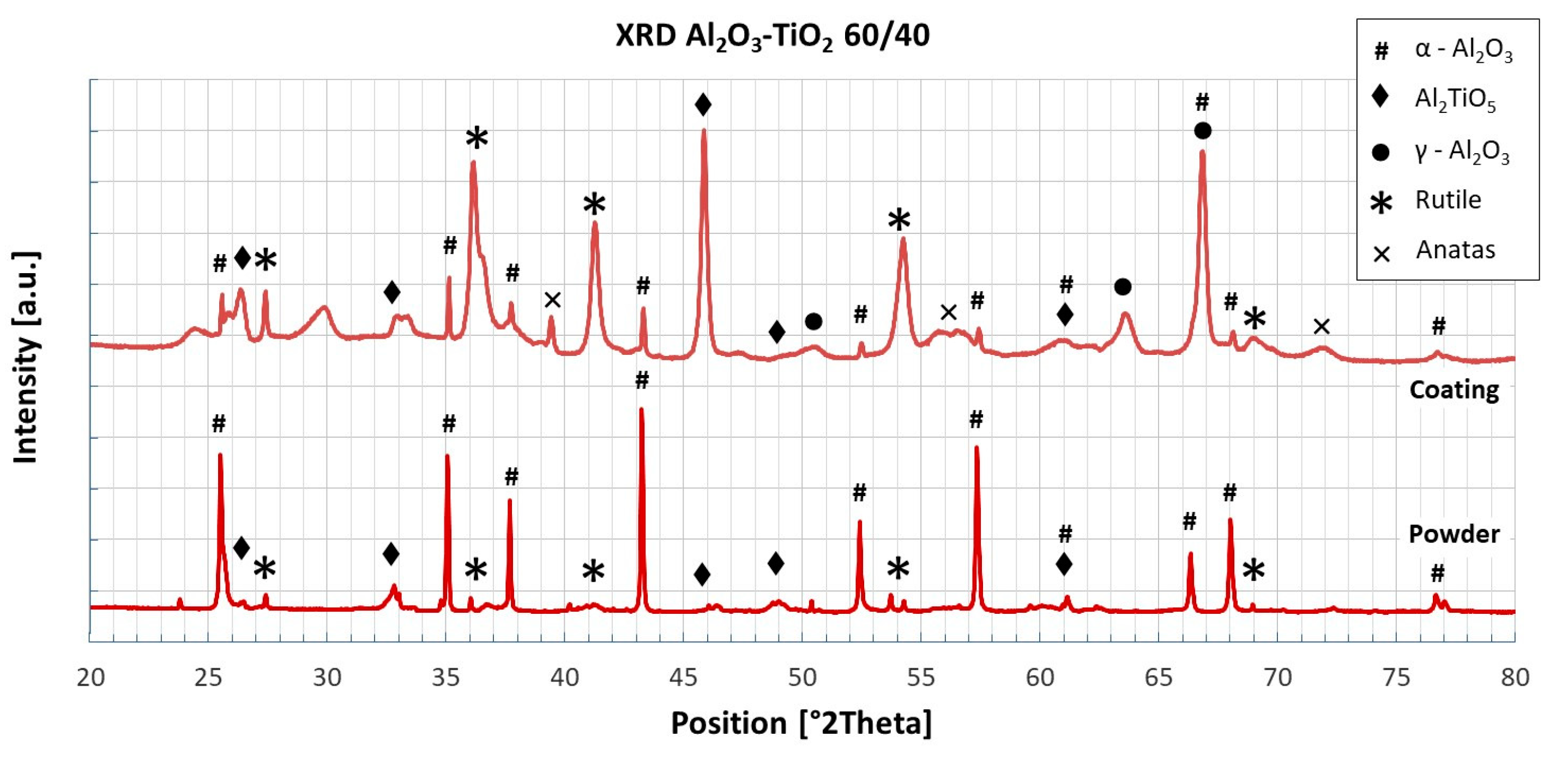
The bond strength was measured according to the pull-off method ISO 14916 with a measuring device on a universal testing machine Zwick Z100 from ZwickRoell GmbH & Co. KG (Ulm, Germany). HTK ULTRA BOND® from HTK Hamburg GmbH (Hamburg, Germany) was used as adhesive and pins with a diameter of 14.2 mm were used as tension rods. Precipitation heat treatment of the glue took place at 190 °C for 35 min. The test speed was set to 0.5 mm/min. The phase composition of APS coatings and spray powder was investigated using the Advance D8 diffractometer from Bruker Corporation (Billerica, MA, USA) with a Cu Kα beam and a graphite monochromator.
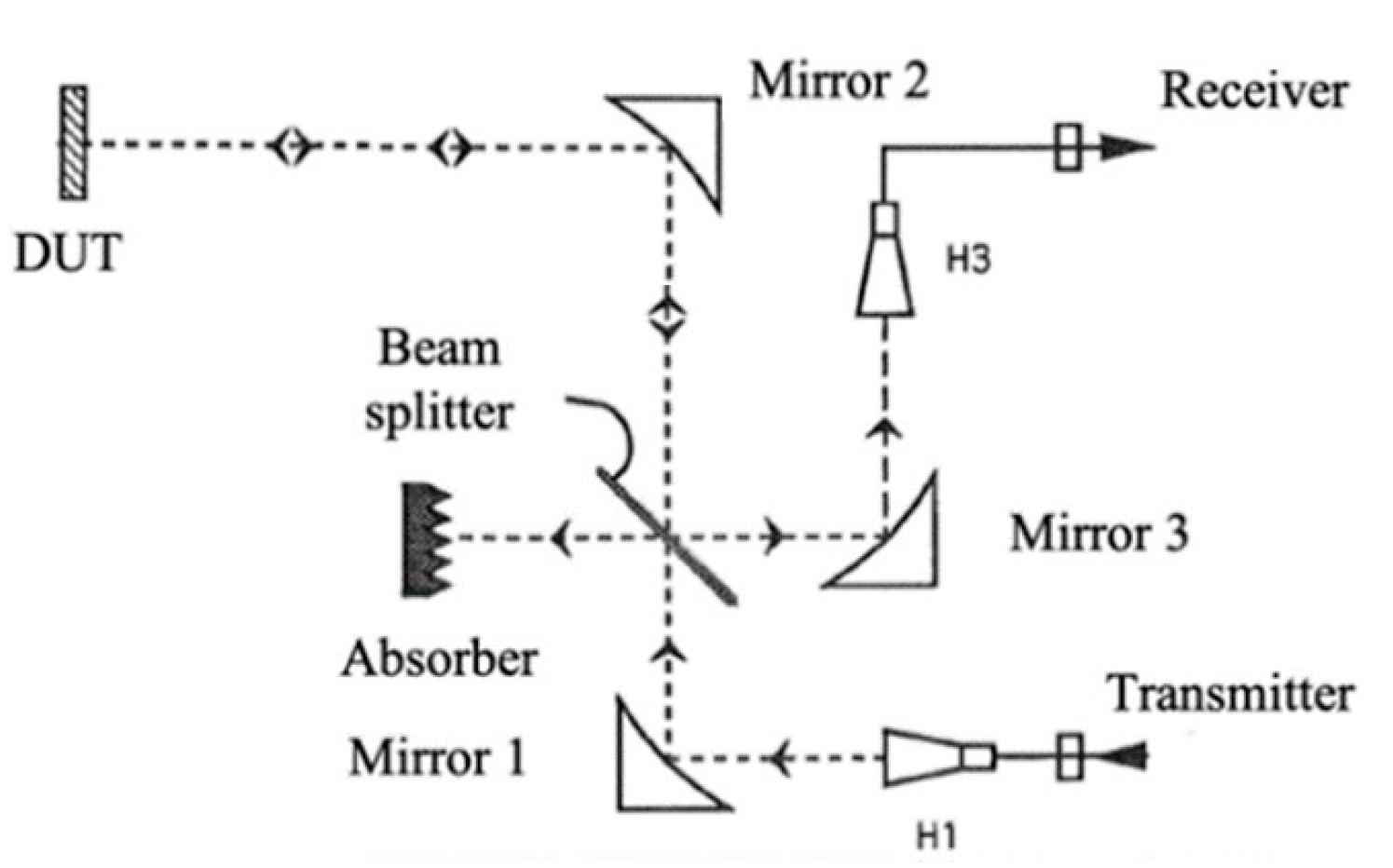
Microwave absorption measurements were performed on flat sample coatings as-sprayed with different thicknesses from 30 μm to 150 μm at 140 GHz and 170 GHz. A schematic view of the reflection measurement setup is shown
Figure 6 [
14]. A millimeter (mm)-wave is transmitted by a corrugated circular horn antenna. The mm-wave is focused on the dielectric coated samples using two mirrors. The reflected signal is separated from the forwarding transmission path using a Mylar foil at 45° angle. The reflected signal is received by a corrugated circular horn antenna and is evaluated by a performance network analyzer (PNA). The frequency range of the PNA is limited up to 26.5 GHz and is increased using extension modules, covering the frequency band from 140–220 GHz.
5. Discussion
Several challenges had to be overcome when applying the internal absorber coating on the dummy load. Realization of a variable coating thickness as a function of the tube length needs some preliminary studies to learn more about the spray conditions that control deposition rate and efficiency as well as coating morphology, i.e., porosity and phase composition inside the tube. These properties are not necessarily the same if compared to coatings produced on small samples under regular conditions. Besides, the manufacturing of an internal coating especially demands a sophisticated temperature guidance by using air lances close to the plasma torch for the internal cooling and additional air knives for outside cooling of the tube surface.
For calibration purposes, test samples have to be manufactured, preferably showing comparable coating properties. With these data in hand, a correlation function of thickness and absorption values can then be derived.
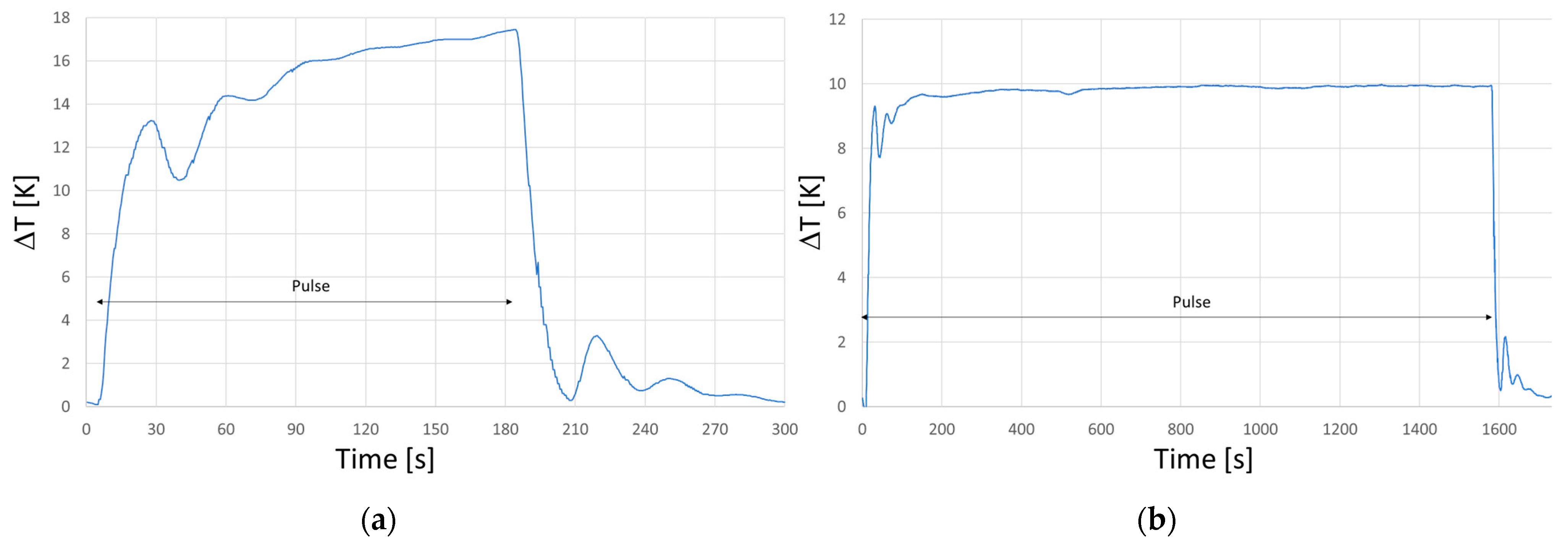
We therefore decided to fabricate the flat samples inside a steel tube to mimic similar process conditions. The cooling concept had to be adapted, as the heat flow of the massive copper tube is much more effective than it is the case in the separated flat copper samples mounted inside the steel tube. During the coating of flat samples, the dummy steel tube reached a maximum temperature of between 120 and 170 °C and the copper samples temperatures between 100 and 130 °C. During the coating of the copper tube, the tube reached a maximum temperature of between 50 and 60 °C. In principle, this has to be taken into account when directly comparing deposition efficiencies and resulting coating thickness during the plasma spray process. On the other hand, the overall temperature levels reached in the process were quite low (100 to 120 °C and 50 to 60 °C, respectively) therefore we do not expect to see strong differences in coating thickness.
Finally, for implementation of a variable coating thickness in the copper tube, several approaches are possible. A continuous change of the coating thickness values could basically be realized by a successive adjustment of the transfer speed of the plasma torch during the coating process. Indeed, this would have made necessary several trials on dummy tubes to exactly work out and adjust the torch and tube kinematic to meet the claimed thickness distribution function. In the present case this was not feasible due to existing cost and time restrictions. The stepwise application of layered coatings therefore represents a good compromise between economic viability and technical requirements. Moreover, this approach is scalable and adjustable to almost any size and thickness gradations.


 ,
, 

