Article

Annealing Studies of Copper Indium Oxide (Cu2In2O5) Thin Films Prepared by RF Magnetron Sputtering

by
Giji Skaria
1,*,
Ashwin Kumar Saikumar
1,
Akshaya D. Shivprasad
2 and
Kalpathy B. Sundaram
1
1
Department of Electrical and Computer Engineering, University of Central Florida, Orlando, FL 32816, USA
2
School of Electrical Engineering and Computer Science, The Pennsylvania State University, University Park, PA 16802, USA
*
Author to whom correspondence should be addressed.
Coatings 2021, 11(11), 1290; https://doi.org/10.3390/coatings11111290
Submission received: 21 September 2021 / Revised: 19 October 2021 / Accepted: 20 October 2021 / Published: 24 October 2021
(This article belongs to the Special Issue Advances in Thin Film Fabrication by Magnetron Sputtering)

Abstract

:
Copper indium oxide (Cu2In2O5) thin films were deposited by the RF magnetron sputtering technique using a Cu2O:In2O3 target. The films were deposited on glass and quartz substrates at room temperature. The films were subsequently annealed at temperatures ranging from 100 to 900 °C in an O2 atmosphere. The X-ray diffraction (XRD) analysis performed on the samples identified the presence of Cu2In2O5 phases along with CuInO2 or In2O3 for the films annealed above 500 °C. An increase in grain size was identified with the increase in annealing temperatures from the XRD analysis. The grain sizes were calculated to vary between 10 and 27 nm in films annealed between 500 and 900 °C. A morphological study performed using SEM further confirmed the crystallization and the grain growth with increasing annealing temperatures. All films displayed high optical transmission of more than 70% in the wavelength region of 500–800 nm. Optical studies carried out on the films indicated a small bandgap change in the range of 3.4–3.6 eV during annealing.

1. Introduction

Transparent conducting oxides (TCOs) have a unique ability to allow visible light to pass through, and to conduct electricity. TCOs find many applications in solar cells, optical displays, reflective coatings, light emission devices, low-emissivity windows, electrochromic mirrors, UV sensors and windows, defrosting windows, electromagnetic shielding, and transparent electronics [1,2,3,4,5,6]. The bulk of research conducted on TCOs involves n-type TCOs for creating devices [7,8,9,10,11,12]. Many transparent electronic applications require the necessity of p-type TCOs. An early attempt to synthesize a p-type TCO from CuAlO2 by the laser ablation method was reported by Kawazoe et al. [13]. Recently, researchers have been looking at the copper indium oxide- and copper gallium oxide-based thin film materials for possible p-type TCO applications [14,15,16,17,18,19,20,21,22,23,24,25,26,27]. Nair et al. fabricated a transparent thin-film p–n junction consisting of Ca and tin-doped CuInO2 [28]. Further, Nair et al. reported the potential use of CuInO2 for thermoelectric applications [29]. Cu2In2O5 is another phase of Cu-In-based oxide. There has not been a lot of work conducted on Cu2In2O5. Synthesis of Cu2In2O5 has been reported only using either smeltering or chemical processes [20,21]. The chemical processes include synthesizing Cu2In2O5 from aqueous solutions of nitrates, chlorides, and sulfates of Cu, In, and Ga [20]. At this moment, there have not been many attempts to investigate Cu2In2O5 deposited by RF magnetron sputtering. RF magnetron sputtering allows films to be deposited with high uniformity and homogeneity as well as providing the capability to control the film thickness and deposition rate [30]. It has an additional advantage of having a low cost as well as the ability to achieve large-area deposition. In this work, the focus was on the deposition of Cu2In2O5 by RF magnetron sputtering using a single target of Cu2O:In2O3 in the ratio of 1:1. The structural and optical properties of Cu2In2O5 thin films were investigated.

2. Experimental Details

2.1. Deposition of Copper Indium Oxide Thin Films

Copper indium oxide films were deposited by a radio frequency magnetron sputtering system using a CTI 100 cryogenic high-vacuum pump. A 600 W, 13.56 MHz RF power supply (Dressler Cesar 136 FST RF Generator, Denver, CO, USA) was used to power the MAK 2 sputter gun (San Jose, CA, USA). The Advance Energy VarioMatch-1000 matching network (Fort Collins, CO, USA) was used to match the source and the load impedance. All the depositions were performed at a power of 50 W. The power was ramped up at the rate of 1 W/s. Glass substrates were used to deposit the films for annealing studies up to 400 °C, whereas quartz substrates were used for annealing studies above 500 °C. The substrates were cleaned with acetone and methanol in an ultrasonic bath followed by rinsing using DI water. The samples were dried with nitrogen gas before loading them into the vacuum system. A 2″ powder pressed target of Cu2O/In2O3 (1/1 mol%, 99.9% purity), ACI Alloy Inc. (San Jose, CA, USA), was used to deposit the films. A gap of 5 cm between the target and the substrate was maintained to achieve a uniform film thickness. A base pressure of 5 × 10⁻⁶ Torr was achieved before initiating the deposition. During the deposition, the pressure was maintained at 10 mTorr with an argon flow of 10 sccm. The deposition rate was found to be approximately 270 Å per minute. This was measured using a Veeco Dektak-150 profilometer (Plainview, NY, USA). All the depositions were conducted for 7.5 min to achieve approximately 2000 Å of film thickness. Post-deposition annealing was conducted from 100 to 900 °C for 90 min in O2 gas flow.

2.2. Characterization of Copper Indium Oxide Thin Films

The XRD measurements were performed using a PANalytical Empyrean XRD system (Malvern Panalytical, Westborough, MA, USA), using radiation from a Cu source at 45 kV and 40 mA. The diffraction patterns were recorded between 2θ angles of 15° and 60°, and the phase information was analyzed using HighScore Plus software (Malvern Panalytical, Westborough, MA, USA). The surface morphology of the film was assessed using a field-emission scanning electron microscope, Zeiss ULTRA-55 FEG SEM (Zeiss Microscopy, White Plains, NY, USA). The optical transmission studies were performed using a Cary 100 UV–Vis spectrophotometer (Varian Analytical Instruments, Walnut Creek, CA, USA).

3. Results and Discussions
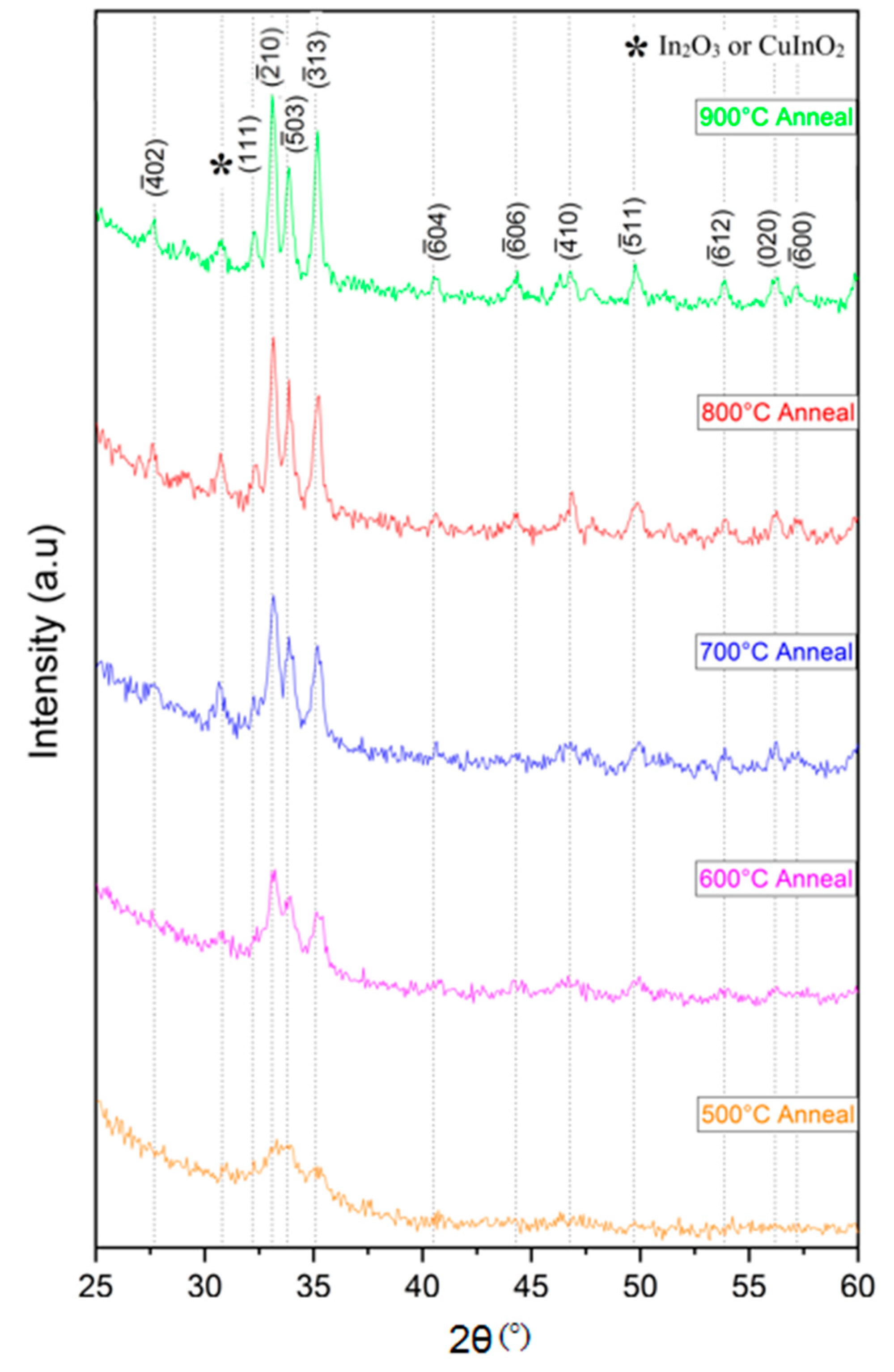
3.1. XRD Analysis

As-deposited films and films annealed up to 400 °C did not reveal any diffraction peaks indicating an amorphous nature. Although the XRD measurement was conducted between 15° and 60°, due to the presence of a broad amorphous peak related to the quartz substrates, the 2θ angle reported in Figure 1 is limited between 25° and 60°. Figure 1 shows the X-ray diffractograms of the films annealed at 500–900 °C in an O2 atmosphere. The film annealed at 500 °C started showing low-intensity peaks related to the ( 2 ¯ 10), ( 5 ¯ 03), and ( 3 ¯ 13) planes that have been attributed to the Cu2In2O5 phase (JCPDSPDF# 30-0479). The films annealed at 600 °C and above showed more peaks related to Cu2In2O5. It was observed that the peak intensity and peak sharpness increased with an increase in annealing temperature, denoting an increase in crystallinity. These identified planes match very well with the Cu2In2O5-synthesized nanoparticles reported by Su et al. [20]. In addition to the Cu2In2O5 phase, a peak at 30.7° (006) was identified. This can be attributed to either the In2O3 or CuInO2 phase [31]. As-deposited films (not shown in Figure 1) did not display any diffraction peaks.
The grain sizes of the films annealed at 500–900 °C were calculated using the Debye–Scherrer equation [32].
D = 0.9 λ β cos θ
where θ is the Bragg angle, β is the full width at half maximum of the peak, λ is the wavelength of the X-ray, and D is the average grain size. The ( 3 ¯ 13) peak was used for the calculation of grain size. The average grain sizes of the Cu2In2O5 films annealed at 500, 600, 700, 800, and 900 °C were calculated to be 10, 13, 17, 21, and 27 nm, respectively.

3.2. Morphology Studies

Figure 2 shows the SEM images of as-deposited Cu2In2O5 thin films as well as those annealed at temperatures varying from 500 to 900 °C. Changes in the morphology were identified for the film annealed at 500–900 °C. As-deposited films and the film annealed at 500 °C displayed the presence of very small grains, as shown in Figure 2a,b. However, the films annealed at 600 °C and above showed an increase in grain size. This coincided with the results from the XRD analysis where the diffraction peaks started to appear for films annealed at 500 °C and above. Both the SEM and the XRD analysis studies indicated that a minimum of 500 °C is required to initiate nanocrystalline growth. Continuous growth in grain size was subsequently observed for the films annealed at 600–900 °C. It is worth mentioning that a pinhole-like appearance was detected in films annealed at 800 and 900 °C. Elemental analysis of all the samples was performed using EDAX incorporated in the FESEM. Nearly equal ratios of Cu:In were identified in all films.

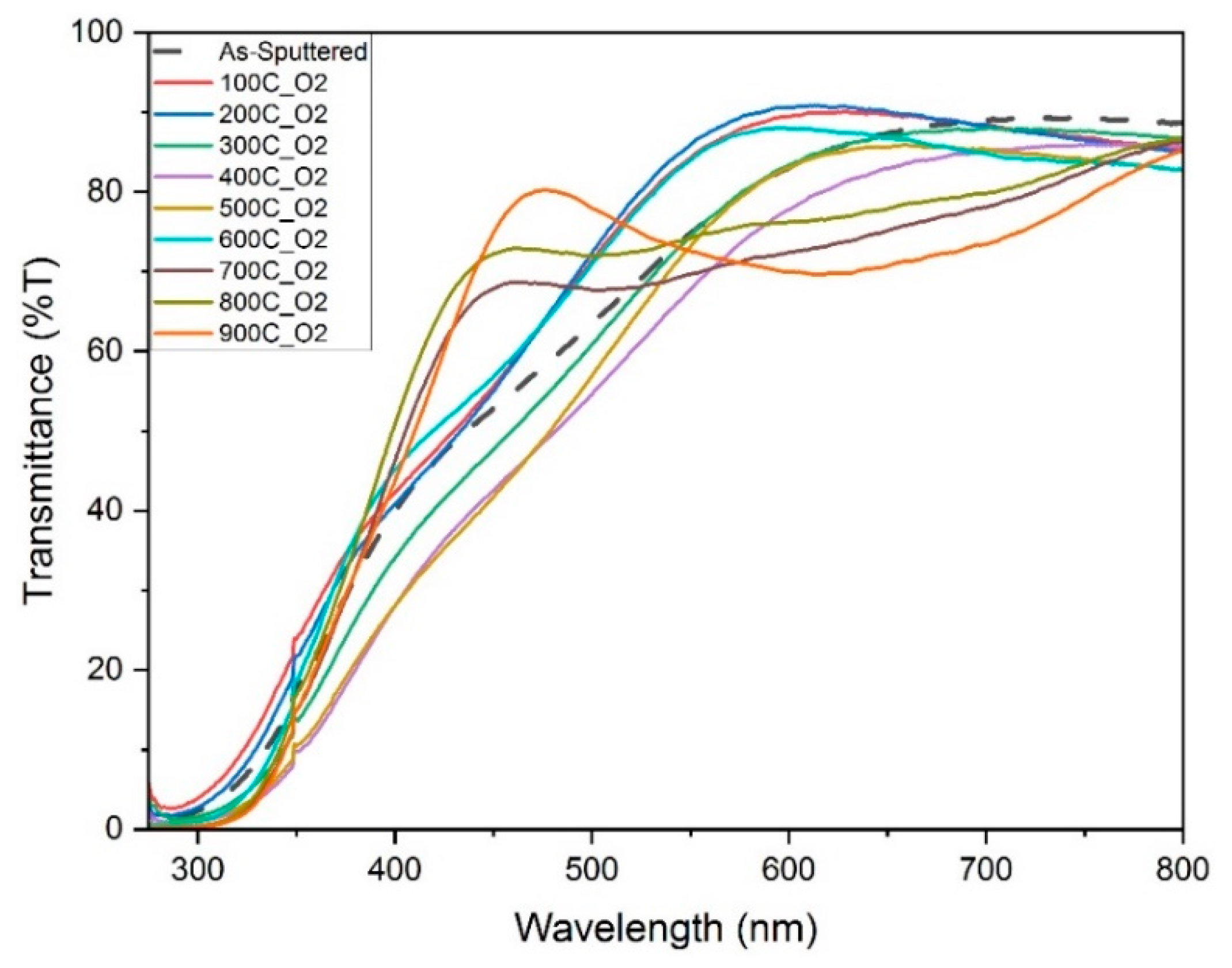
3.3. Optical Studies

A Cary 100 UV–Vis spectrophotometer (Agilent Technologies, Santa Clara, CA, USA) was used to perform the optical characterization of the annealed Cu2In2O5 thin films. Figure 3 shows the percent of transmission for the films deposited on glass and quartz substrates and subsequently annealed from 100 to 900 °C. Overall, the optical transmission increased for the films annealed at different temperatures. The transmission values of the annealed films were observed to vary between 70% and 90%. At a 450 nm wavelength, the films annealed at 900 °C displayed the highest transmission of 80%. However, the films annealed at 900 °C subsequently showed a decreasing trend in transmission beyond a 500 nm wavelength. This could possibly be attributed to an increase in grain size with annealing, as reported in [33,34].

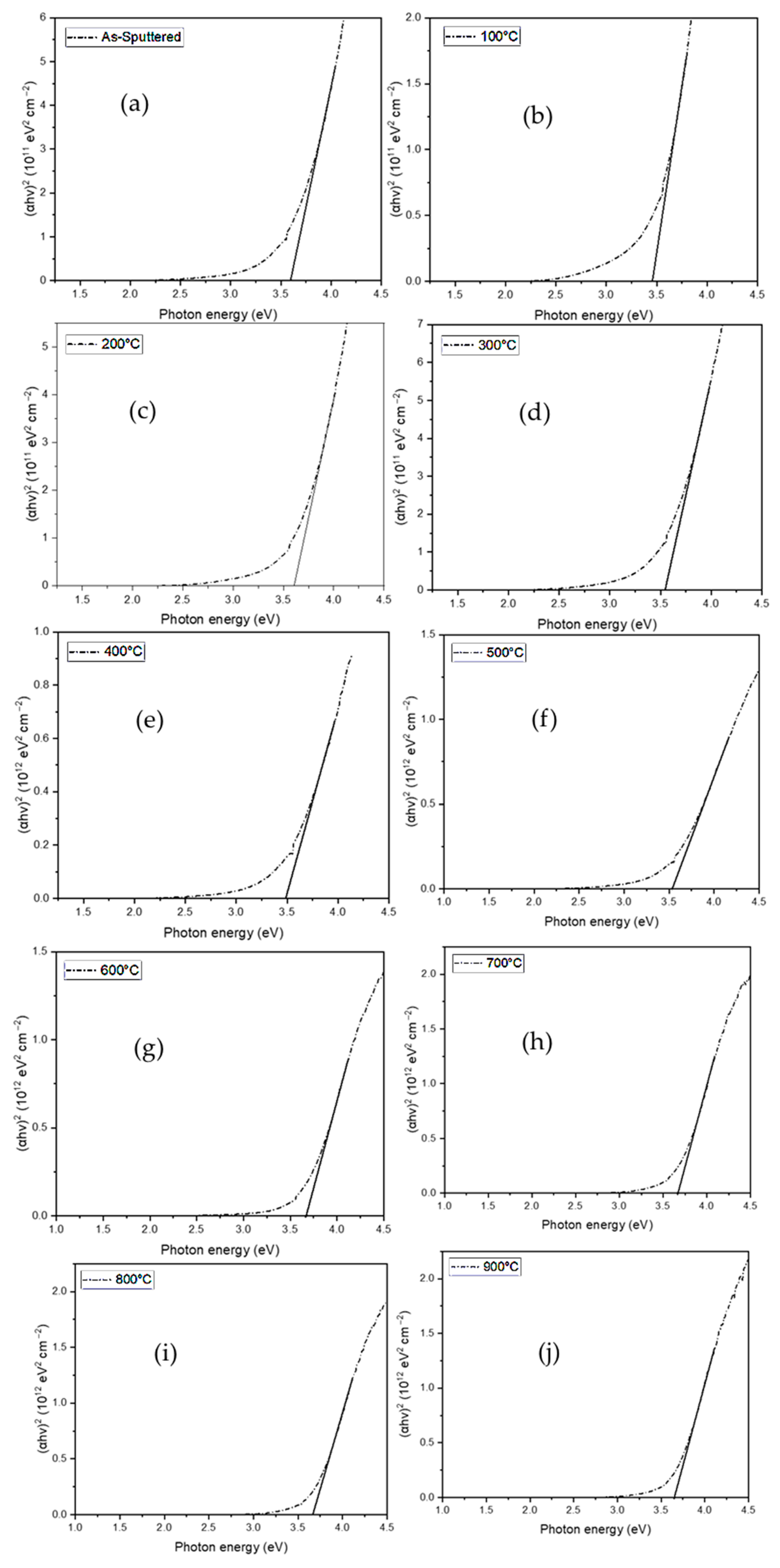
3.4. Optical Bandgap

The optical transmission data were used to calculate the optical band gap of Cu2In2O5 thin films using the Tauc plot method [35,36,37]. Since the reflectance was identified to be less than 5%, the absorption coefficient α was calculated directly from the transmission data [36]. The absorption coefficient α was calculated using Equation (2), where d is the thickness of the film, and T is the percent of transmission. The optical bandgap (Eg) was estimated from Equation (3).
α = 1 d ln ( 1 T )
(αhν)1/n = B(hν − Eg)
where hν is the photon energy, B is a constant, Eg is the optical bandgap, and n = 1/2 for the direct bandgap transition. Figure 4a–j show the Tauc plot generated using the above equations. The linear region of the curve was extrapolated to the x-axis to identify the Eg value. The extrapolated values of the bandgap are listed in Table 1. The bandgap for Cu2In2O5 thin films is reported for the first time in this work. The bandgap was in the range of 3.4–3.6 eV. It is worth mentioning that an increase in the annealing temperature did not have any major effect on the bandgap.

4. Conclusions

Cu2In2O5 thin films were deposited by the RF magnetron sputtering technique. The effects of structural, morphological, and optical properties due to post-deposition annealing at 100–900 °C with a constant O2 flow were studied. Both the XRD analysis and the FESEM images concluded that a minimum annealing temperature of 500 °C was required to initiate the crystallization and grain growth. A further increase in the annealing temperature resulted in an increase in crystallization and grain size. The largest average grain size was observed in films annealed at 900 °C. In addition to the Cu2In2O5 phases, the XRD results reveal the presence of an additional phase corresponding to either In2O3 or CuInO2. Optical studies showed a bandgap of 3.4–3.6 eV for the films.

Author Contributions

Conceptualization, G.S. and K.B.S.; methodology, G.S. and A.K.S.; validation, G.S. and A.D.S.; formal analysis, G.S., A.K.S. and K.B.S.; data curation, G.S., A.K.S. and K.B.S.; writing—original draft preparation, G.S. and K.B.S.; writing—review and editing, G.S., A.K.S. and K.B.S.; visualization, G.S. and A.K.S.; supervision, K.B.S.; project administration, K.B.S. All authors have read and agreed to the published version of the manuscript.

Funding

Article processing charges were provided in part by the UCF College of Graduate Studies Open Access Publishing Fund.

Institutional Review Board Statement

Not applicable.

Informed Consent Statement

Not applicable.

Data Availability Statement

Not applicable.

Conflicts of Interest

The authors declare no conflict of interest.

References

  1. Chopra, K.; Major, S.; Pandya, D. Transparent conductors—A status review. Thin Solid Film. 1983, 102, 1–46. [Google Scholar] [CrossRef]
  2. Dawar, A.; Joshi, J. Semiconducting transparent thin films: Their properties and applications. J. Mater. Sci. 1984, 19, 1–23. [Google Scholar] [CrossRef]
  3. Gordon, R.G. Criteria for choosing transparent conductors. MRS Bull. 2000, 25, 52–57. [Google Scholar] [CrossRef] [Green Version]
  4. Saikumar, A.K.; Skaria, G.; Sundaram, K.B. ZnO gate based MOSFETs for sensor applications. ECS Trans. 2014, 61, 65. [Google Scholar] [CrossRef]
  5. Szyszka, B.; Loebmann, P.; Georg, A.; May, C.; Elsaesser, C. Development of new transparent conductors and device applications utilizing a multidisciplinary approach. Thin Solid Film. 2010, 518, 3109–3114. [Google Scholar] [CrossRef]
  6. Zhang, B.; Yu, B.; Jin, J.; Ge, B.; Yin, R. Performance of InSnZrO as transparent conductive oxides. Phys. Status Solidi 2010, 207, 955–962. [Google Scholar] [CrossRef]
  7. Khan, A.; Rahman, F. Study of microstructural and optical properties of nanocrystalline indium oxide: A transparent conducting oxide (TCO). AIP Conf. Proc. 2019, 2115, 030091. [Google Scholar]
  8. Nehate, S.D.; Prakash, A.; Mani, P.D.; Sundaram, K.B. Work function extraction of indium tin oxide films from MOSFET devices. ECS J. Solid State Sci. Technol. 2018, 7, P87. [Google Scholar] [CrossRef]
  9. Sundaram, K.; Khan, A. Work function determination of zinc oxide films. J. Vac. Sci. Technol. A Vac. Surf. Film. 1997, 15, 428–430. [Google Scholar] [CrossRef]
  10. Sundaram, K.; Khan, A.J.T.S.F. Characterization and optimization of zinc oxide films by RF magnetron sputtering. Thin Solid Film. 1997, 295, 87–91. [Google Scholar] [CrossRef]
  11. Sundaresh, S.; Nehate, S.D.; Sundaram, K.B. Electrical and optical studies of reactively sputtered indium oxide thin films. ECS J. Solid State Sci. Technol. 2021, 10, 065016. [Google Scholar] [CrossRef]
  12. Noh, J.H.; Ryu, S.Y.; Jo, S.J.; Kim, C.S.; Sohn, S.-W.; Rack, P.D.; Kim, D.-J.; Baik, H.K. Indium oxide thin-film transistors fabricated by RF sputtering at room temperature. IEEE Electron. Device Lett. 2010, 31, 567–569. [Google Scholar] [CrossRef]
  13. Kawazoe, H.; Yasukawa, M.; Hyodo, H.; Kurita, M.; Yanagi, H.; Hosono, H.J.N. P-type electrical conduction in transparent thin films of CuAlO2. Nat. Cell Biol. 1997, 389, 939–942. [Google Scholar] [CrossRef]
  14. Biswas, S.K.; Sarkar, A.; Pathak, A.; Pramanik, P.J.T. Studies on the sensing behaviour of nanocrystalline CuGa2O4 towards hydrogen, liquefied petroleum gas and ammonia. Talanta 2010, 81, 1607–1612. [Google Scholar] [CrossRef]
  15. Fenner, L.; Wills, A.; Bramwell, S.; Dahlberg, M.; Schiffer, P. Zero-point entropy of the spinel spin glasses CuGa2O4 and CuAl2O4. J. Phys. Conf. Ser. 2008, 145, 012029. [Google Scholar] [CrossRef] [Green Version]
  16. Makhova, L.; Wett, D.; Lorenz, M.; Konovalov, I. X-ray spectroscopic investigation of forbidden direct transitions in CuGaO2 and CuInO2. Phys. Status 2006, 203, 2861–2866. [Google Scholar] [CrossRef]
  17. Pilliadugula, R.; Nithya, C.; Krishnan, N.G.; Nammalwar, G. Influence of Ga2O3, CuGa2O4 and Cu4O3 phases on the sodium-ion storage behaviour of CuO and its gallium composites. Nanoscale Adv. 2020, 2, 1269–1281. [Google Scholar] [CrossRef] [Green Version]
  18. Saikumar, A.K.; Sundaresh, S.; Nehate, S.D.; Sundaram, K.B.J.C. Properties of RF magnetron-sputtered copper gallium oxide (CuGa2O4). Thin Film. 2021, 11, 921. [Google Scholar]
  19. Shi, J.; Liang, H.; Xia, X.; Li, Z.; Long, Z.; Zhang, H.; Liu, Y. Preparation of high-quality CuGa2O4 film via annealing process of Cu/β-Ga2O3. J. Mater. Sci. 2019, 54, 11111–11116. [Google Scholar] [CrossRef]
  20. Su, C.-Y.; Chiu, C.-Y.; Chang, C.-H.; Ting, J.-M. Synthesis of Cu2In2O5 and CuInGaO4 nanoparticles. Thin Solid Film. 2013, 531, 42–48. [Google Scholar] [CrossRef]
  21. Su, C.-Y.; Mishra, D.K.; Chiu, C.-Y.; Ting, J.-M. Effects of Cu2S sintering aid on the formation of CuInS2 coatings from single crystal Cu2In2O5 nanoparticles. Surf. Coat. Technol. 2013, 231, 517–520. [Google Scholar] [CrossRef]
  22. Wang, J.; Ibarra, V.; Barrera, D.; Xu, L.; Lee, Y.-J.; Hsu, J.W.P. Solution synthesized p-type copper gallium oxide nanoplates as hole transport layer for organic photovoltaic devices. J. Phys. Chem. Lett. 2015, 6, 1071–1075. [Google Scholar] [CrossRef] [PubMed]
  23. Wei, H.; Chen, Z.; Wu, Z.; Cui, W.; Huang, Y.; Tang, W. Epitaxial growth and characterization of CuGa2O4 films by laser molecular beam epitaxy. AIP Adv. 2017, 7, 115216. [Google Scholar] [CrossRef] [Green Version]
  24. Yin, H.; Shi, Y.; Dong, Y.; Chu, X. Synthesis of spinel-type CuGa2O4 nanoparticles as a sensitive non-enzymatic electrochemical sensor for hydrogen peroxide and glucose detection. J. Electroanal. Chem. 2021, 885, 115100. [Google Scholar] [CrossRef]
  25. Zardkhoshoui, A.M.; Davarani, S.S. Designing a flexible all-solid-state supercapacitor based on CuGa2O4 and FeP-rGO electrodes. J. Alloys Compd. 2019, 773, 527–536. [Google Scholar] [CrossRef]
  26. Zhang, K.H.L.; Xi, K.; Blamire, M.; Egdell, R.G. P-type transparent conducting oxides. J. Phys. Condens. Mater. 2016, 28, 383002. [Google Scholar] [CrossRef]
  27. Singh, M.; Singh, V.N.; Mehta, B.R. Synthesis and properties of nanocrystalline copper indium oxide thin films deposited by RF magnetron sputtering. J. Nanosci. Nanotechnol. 2008, 8, 3889–3894. [Google Scholar] [CrossRef] [PubMed]
  28. Nair, B.G.; Rahman, H.; Aijo, J.K.; Keerthi, K.; Shaji, G.S.O.; Sharma, V.; Philip, R.R. Calcium incorporated copper indium oxide thin films—A promising candidate for transparent electronic applications. Thin Solid Film. 2019, 693, 137673. [Google Scholar] [CrossRef]
  29. Nair, B.G.; Okram, G.S.; Naduvath, J.; Shripathi, T.; Fatima, A.; Patel, T.; Jacob, R.; Keerthi, K.; Remillard, S.K.; Philip, R.R. Low temperature thermopower and electrical conductivity in highly conductive CuInO2 thin films. J. Mater. Chem. C 2014, 2, 6765–6772. [Google Scholar] [CrossRef]
  30. Saikumar, A.K.; Nehate, S.D.; Sundaram, K.B. Review—RF sputtered films of Ga2O3. ECS J. Solid State Sci. Technol. 2019, 8, Q3064–Q3078. [Google Scholar] [CrossRef]
  31. Yang, B.; He, Y.; Polity, A.; Meyer, B.K. Structural, optical and electrical properties of transparent conducting CuInO2 thin films prepared by RF sputtering. MRS Proc. 2005, 865, 865. [Google Scholar] [CrossRef]
  32. Holzwarth, U.; Gibson, N. The Scherrer equation versus the ‘Debye-Scherrer equation’. Nat. Nanotechnol. 2011, 6, 534. [Google Scholar] [CrossRef] [PubMed]
  33. Ramana, C.V.; Smith, R.J.; Hussain, O.M. Grain size effects on the optical characteristics of pulsed-laser deposited vanadium oxide thin films. Phys. Status 2003, 199, R4–R6. [Google Scholar] [CrossRef]
  34. Shakti, N.; Gupta, P. Structural and optical properties of sol-gel prepared ZnO thin film. Appl. Phys. Res. 2010, 2, 19. [Google Scholar] [CrossRef] [Green Version]
  35. Duta, M.; Anastasescu, M.; Calderon-Moreno, J.M.; Predoana, L.; Preda, S.; Nicolescu, M.; Stroescu, H.; Bratan, V.; Dascalu, I.; Aperathitis, E.; et al. Sol–gel versus sputtering indium tin oxide films as transparent conducting oxide materials. J. Mater. Sci. Mater. Electron. 2016, 27, 4913–4922. [Google Scholar] [CrossRef]
  36. Spence, W. The UV absorption edge of tin oxide thin films. J. Appl. Phys. 1967, 38, 3767–3770. [Google Scholar] [CrossRef]
  37. Lv, J.; Huang, K.; Chen, X.; Zhu, J.; Cao, C.; Song, X.; Sun, Z. Optical constants of Na-doped ZnO thin films by sol-gel method. Opt. Commun. 2011, 284, 2905–2908. [Google Scholar] [CrossRef]
Figure 1. X-ray diffraction of the films annealed at 500–900 °C in O2 for 90 min.
Coatings 11 01290 g001
Figure 2. SEM images of Cu2In2O5 films (a) as deposited and annealed at (b) 500 °C, (c) 600 °C, (d) 700 °C, (e) 800 °C, and (f) 900 °C.
Coatings 11 01290 g002
Figure 3. Optical transmission spectra of the Cu2In2O5 thin films annealed at various temperatures.
Coatings 11 01290 g003
Figure 4. (aj): Tauc plots of the Cu2In2O5 thin films annealed at different temperatures.
Coatings 11 01290 g004
Table 1. Optical bandgap values obtained for Cu2In2O5 thin films.
Annealing Temperature ( °C)Bandgap (eV)
As deposited3.59
1003.45
2003.6
3003.54
4003.48
5003.53
6003.66
7003.66
8003.66
9003.64
Publisher’s Note: MDPI stays neutral with regard to jurisdictional claims in published maps and institutional affiliations.

