1. Introduction
In silicon heterojunction (SHJ) solar cells, the hydrogenated amorphous silicon (a-Si:H) thin layer is too low in transverse conductivity to collect charge carriers horizontally over the metal electrodes effectively. Additional transparent conductive oxide layers such as Sn-doped In
2O
3 (ITO) are deposited at the top. In addition to charge collection, another essential function of the front-end transparent conductive oxide (TCO) layer is to act as an anti-reflective layer. Because ITO has excellent performance with low resistivity and high transparency, ITO is currently the most widely used transparent conductive oxide [
1]. However, In
2O
3 has the disadvantage of high refining and production costs and the relative scarcity of indium ore. Sn is also susceptible to price fluctuations (compared to other elements (e.g., Zn). Finding a replacement for ITO could reduce the costs of the production of SHJ solar cells. Aluminum-doped zinc oxide (AZO) is based on zinc oxide. Zinc oxide (ZnO) is a potential candidate in TCO, known as ZnO, a natural type of semiconductor with an energy gap of 3.4 eV (intrinsic n-type semiconductor) [
2]. Compared with ITO, AZO has high thermal stability and a low price, and is mineral-rich, relatively non-toxic, and has an increased transparency of the visible light range, as well as other advantages [
3,
4,
5,
6].
As mentioned above, reducing costs and improving conversion efficiency have always been the solar cell industry’s theme. With the continuous progress of solar cell industry technology and policy promotion, the public’s attention gradually shifted to the cost of electricity, and high-efficiency batteries have attracted attention. The three high costs of SHJ cells are for the silicon chip, conductive silver paste, and target material. Because of these three high-cost components, various cost reductions will help improve SHJ cells’ competitiveness, including reducing the consumption of raw materials and introducing new technologies.
In SHJ technology, the low-temperature silver paste is used. Still, the conductivity of low-temperature silver paste is significantly lower than that of bulk silver, so the conductivity of silver electrodes in SHJ solar cells is lower than that of silver electrodes in c-Si solar cells. Therefore, the use of silver paste in a typical 3–5 bus configuration limits efficiency and increases the cost of SHJ solar cells, estimated to cost 30% due to the use of a large number of expensive low-temperature net-printed silver paste processes. The electroplating technology can effectively reduce the cost of electrodes. The Cu metallization process introduces to SHJ solar cells, and it is crucial to improve the SHJ solar cell industry’s competitiveness. At present, there are some reports on the application of copper plating technology to SHJ solar cells [
7,
8,
9,
10].
Li et al. used a rotating coating method to coat the resin (photo-resistance) on the n-type 156 mm SHJ surface [
10]. Then pattern the resin by the inkjet printer (Dimatix DMP 2800). Copper is then plated to the p-i type a-Si: H’s ITO surface using field-induced power generation plating (FIP). The efficiency of the SHJ solar cells produced by Li is 18.8% (Voc s 717 mV, Jsc s 35.4 mA/cm
2, and F.F. s 74%). Dabirian et al. introduced the double-mask layer strategy for the metallization of SHJ solar cells. They combined the nanosecond laser patterning and Ni-Cu electroplating. The results showed that the Ni-Cu metallization qualities of their process are comparable to Ag screen-printing and lithography-based Cu plating [
11]. Meza et al. compared ZnO:Al films instead of the usual ITO as the front TCO in rear emitter SHJ solar cells. An indium-free mono facial cell achieved η = 22.5% showing that the replacement of ITO/Ag by ZnO:Al/Ag as a back contact produces cells with practically the same efficiency [
12].
In SHJ technology, the metallic contacts are generally deposited on a transparent conductive oxide (TCO). Contact metallization on TCOs is typically performed by screen-printing of low-temperature Ag pastes. Electroplating of copper is becoming more attractive to reduce precious Ag consumption. However, copper has a high diffusion coefficient and high solubility in silicon and formation copper silicide at low temperature. TCO can also serve as a barrier to Cu migration. Additionally, the Cu directly electroplated on TCO is usually tricky. Kang et al. also reported the electroplated copper films fail to adhere to Si during rapid heating and cooling [
13]. Thus, an additional seed layer is usually used. The plating process sequence involves seed layers usually deposited by physical vapor deposition (PVD). Additionally, copper electroplating by the D.C. power supplier is the most commonly adopted method.
Li et al. and Dabirian et al. confirmed that the plated copper process could be applied to SHJ solar cells. However, their reports focused on the electroplating Ni-Cu (or Cu) on ITO [
10,
11]. Meza et al. showed that the ITO/Ag could be replaced by ZnO:Al/Ag [
12]. There have been no reports about the electroplating Cu on AZO till now. Additionally, about the role of seed copper layer on AZO. In this work, we studied the thermal stability of the copper seed layer and the AZO layer on the textured silicon.
2. Materials and Methods
As substrate, commercially available single crystal phosphorus-doped (0 0 1) oriented silicon wafers with textured roughness around 3–5 μm were used. The acetone and H2SO4/H2O2 solution were applied to clean the textured silicon substrate. To remove the native oxide of the silicon, the substrate dip into hydrogen fluoride solution before loading into the vacuum chamber. The AZO and copper films were sputter-deposited onto textured silicon substrates in a direct current/radio-frequency (dc/rf) magnetron sputtering system. The AZO films were sputtered from an AZO target with an rf power supply in an Ar ambient of 99.999% purity. The base pressure of the vacuum chamber was 2 × 10⁻⁷ Torr. The rf power was held at 60 W during deposition. Additionally, a fixed Ar flow rate and the operation pressure were 50 sccm and 6 × 10⁻³ Torr, respectively. A fixed Ar flow rate of 25 sccm and the dc power held at 30 W during the copper film deposition. The AZO and copper films were deposited onto a textured silicon substrate at 25 °C during the sputtering process. The sputtered AZO and copper films’ thicknesses were 65 nm and 220 nm, respectively. AZO films and copper films were subsequently sputter-deposited without breaking the vacuum. The samples are designed for Cu/AZO/Si.
To evaluate the copper seed layer and the barrier property of the AZO layer, an annealing temperature from 300 to 800 °C was selected. The as-deposited samples were annealed in the furnace at 300–800 °C for 10 min in an Ar/H2 atmosphere. The structure was obtained using a scanning electron microscope (SEM, JEOL Ltd., Tokyo, Japan) and a scanning transmission electron microscope (STEM, JEOL Ltd. L, Tokyo, Japan). SEM and STEM were performed on JSM-6360 and a JEM-ARM200, respectively. A STEM that was equipped with an energy dispersive X-ray spectrometer (EDS, Oxford Instruments, Abingdon, UK) was used to determine the chemical composition and STEM-EDS compositional maps of all samples. A focus ion beam (FIB) resembled a scanning electron microscope (SEM) operating at 20 kV and was used for a cross-sectional view of SEM examination. The sample’s surface is protected with an about 2 µm Pt layer formed by an electron beam within the FIB chamber. The sample was then ion-milled using a focused beam of gallium ions to give a cross-section view. The tape and peel-off tests were conducted on the as-deposited sample. For the tape and peel-off tests, about 15 µm thick copper layer was deposited on the Cu/AZO/Si by electroplating. Tape tests were conducted by peeling the 3 M Scotch tape off at 180°. The peel-off tests were conducted at an angle of 180° with a constant speed of 30 mm/min.
3. Results and Discussion
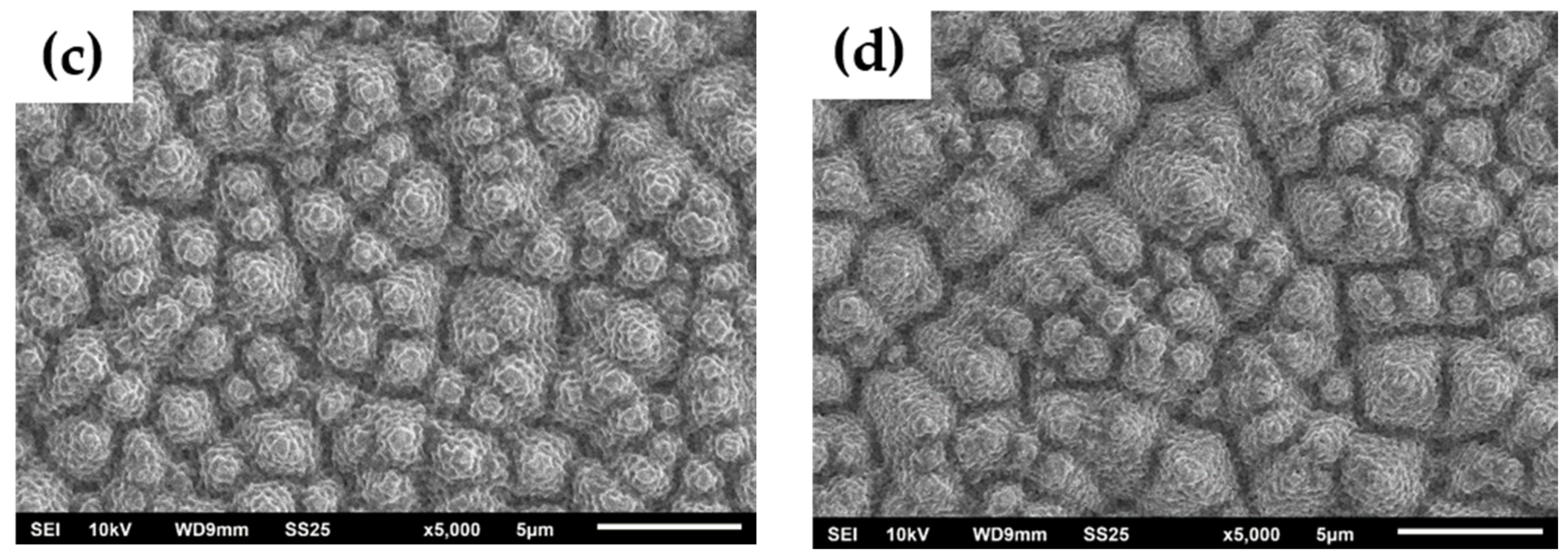
SEM images for the Cu/AZO/Si samples annealed at 300, 500, 600, and 800 °C are presented in
Figure 1. The pyramid shapes with uniform Cu and AZO thin layers exist on the surface of the samples after annealing at 300 °C (
Figure 1a). The surface is smooth for the annealing of the samples at temperatures 300 °C. The surface of the as-deposited sample is the same as the sample annealing at 300 °C for 10 min. The surface became rough when the annealing temperature was higher than 500 °C, as shown in
Figure 1b–d.
The cross-sectional views of SEM for the Cu/AZO/Si samples annealed at 400, 600, and 800 °C are shown in
Figure 2. The copper thin films were continuous for all samples. However, the thin films (Cu/AZO or Cu) were detached from the substrate (silicon or AZO/Si substrate) in some areas for the samples after 400 °C annealing. It was hard to know the composition of the detached thin film (Cu/AZO or Cu) from FIB-SEM. Additionally, the separation of thin films and silicon substrate (or AZO/Si) became severe at temperatures of 600 and 800 °C. It was also hard to confirm the gap formed at the Cu and AZO/Si or Cu/AZO and silicon interfaces.
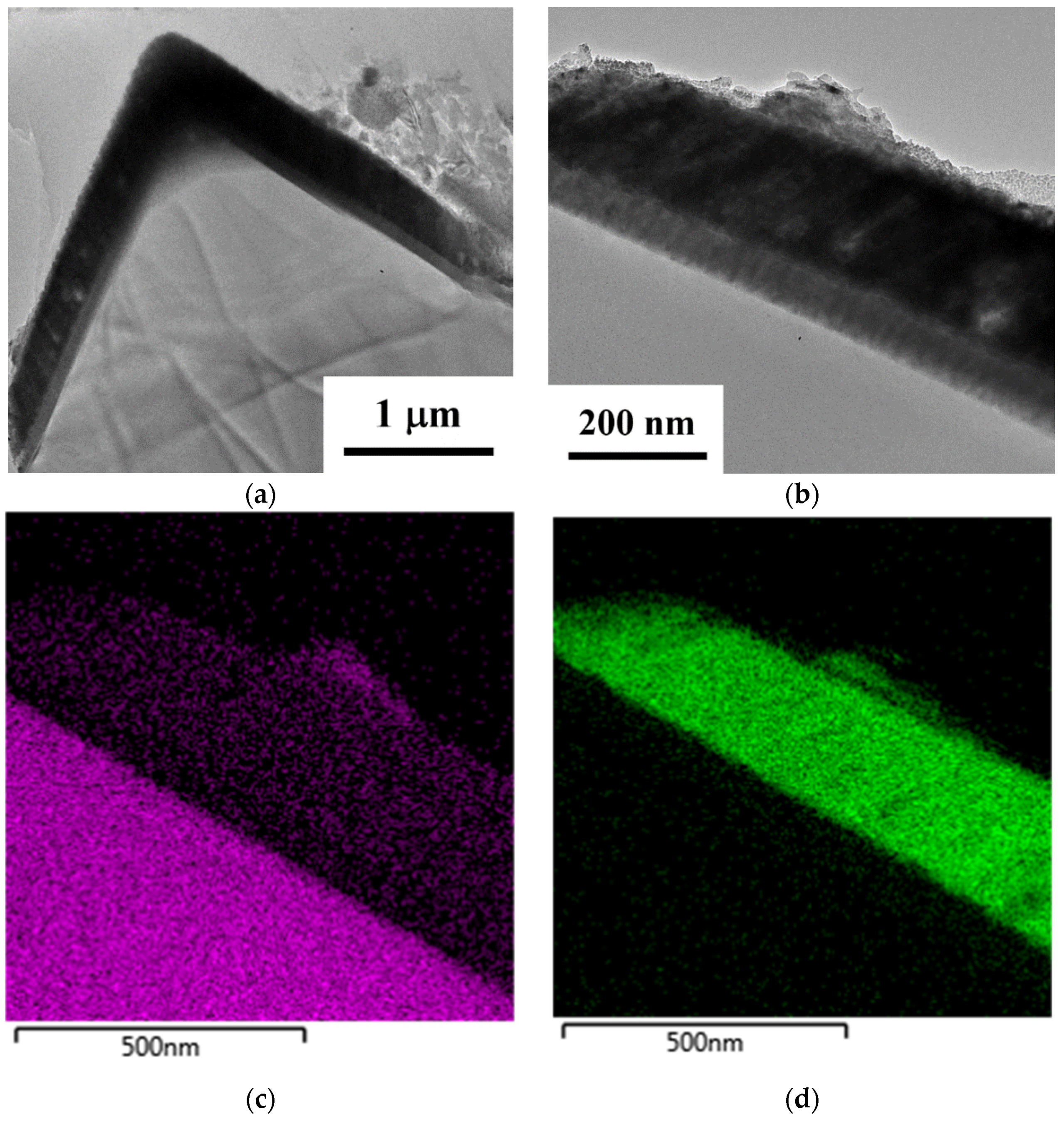
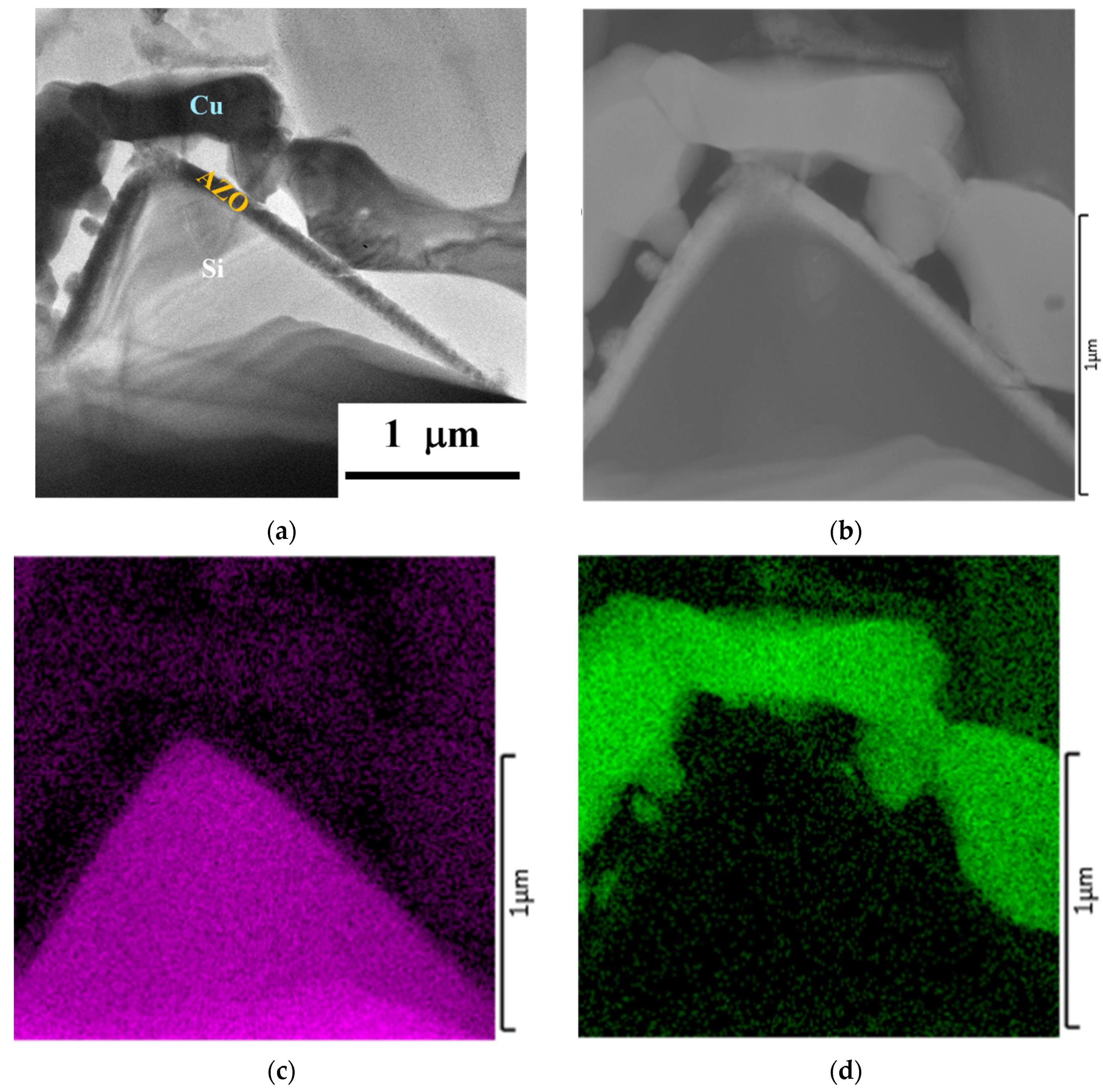
The low and high magnification TEM micrographs of Cu/AZO/Si sample annealed at 300 °C are shown in
Figure 3a,b, respectively. The multilayer is preserved after annealing at 300 °C for 10 min. The structure of the as-deposited sample is the same as the sample annealing at 300 °C for 10 min.
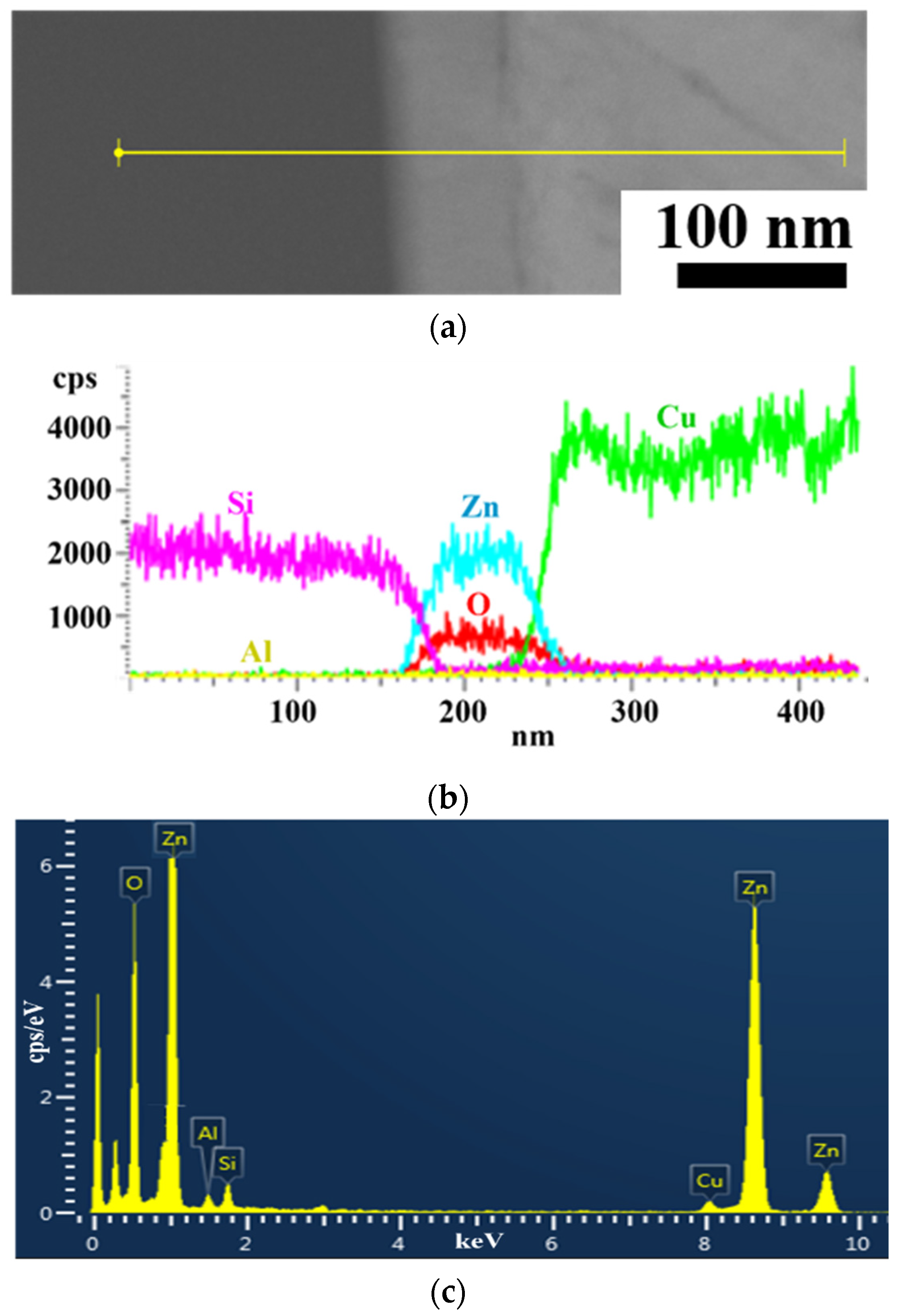
Figure 3c–f shows the EDS maps of Si, Cu, Zn, and O, respectively. The Zn and O elements are overlapped and located between the copper and silicon elements. The elemental maps reveal that the Cu/AZO/Si stack structure is very stable after annealing at 300 °C for 10 min. The line scan across the Cu/AZO/Si using STEM-EDS is shown in
Figure 4a.
Figure 4b shows the intensity signal of the Si, Zn, O, Al, and Cu elements along the yellow line, shown in
Figure 4a. The signal of the aluminum element is almost at the noise level due to the small aluminum amount in the AZO layer. The spot analysis of the AZO layer is shown in
Figure 4c. The amount of aluminum is only about 1.3 at.%. The distribution of zinc and oxygen in the Cu/AZO/Si stack is located at a scale between 180 and 245 nm, which reveals that the thickness of the AZO layer is near 65 nm. There were interfacial layers at the scale of 165–190 nm and 235–260 nm (
Figure 4b). The width of the interface layer was caused by the situation where the interface plane was not perpendicular to the figure shown in
Figure 4a. The thickness of the AZO thin film is also near 65 nm, from
Figure 3b–f. The thickness of the copper thin film is about 220 nm, as shown in
Figure 3b,d. Only a silicon signal emerges at a scale below 160 nm. Additionally, the copper signal was presented at a scale almost greater than 260 nm. The line scan shows that Cu/AZO/Si structure is maintained after annealing at 300 °C. The result of the line scan (
Figure 4) agrees with the work of the TEM and EDS map (
Figure 3).
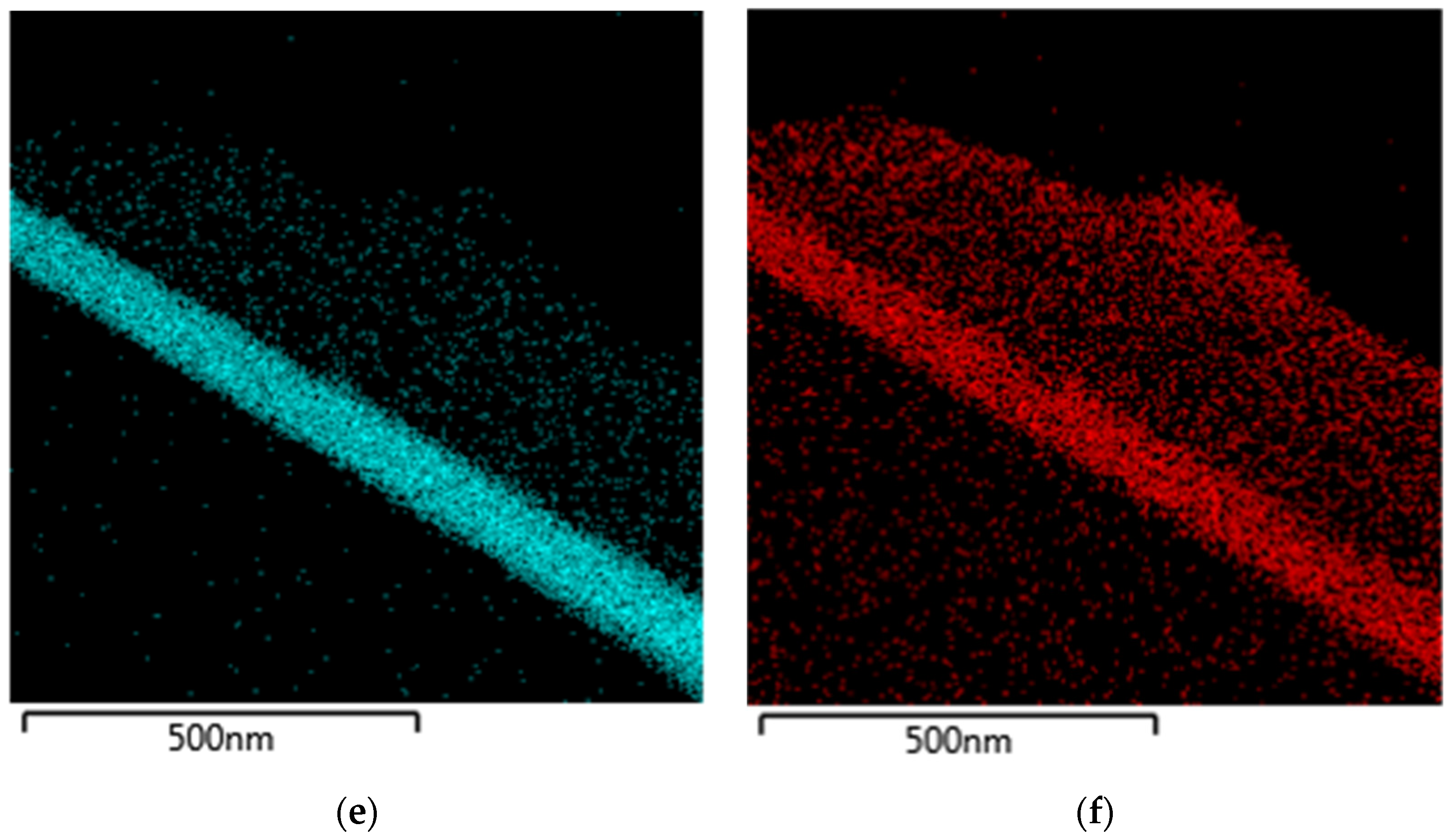
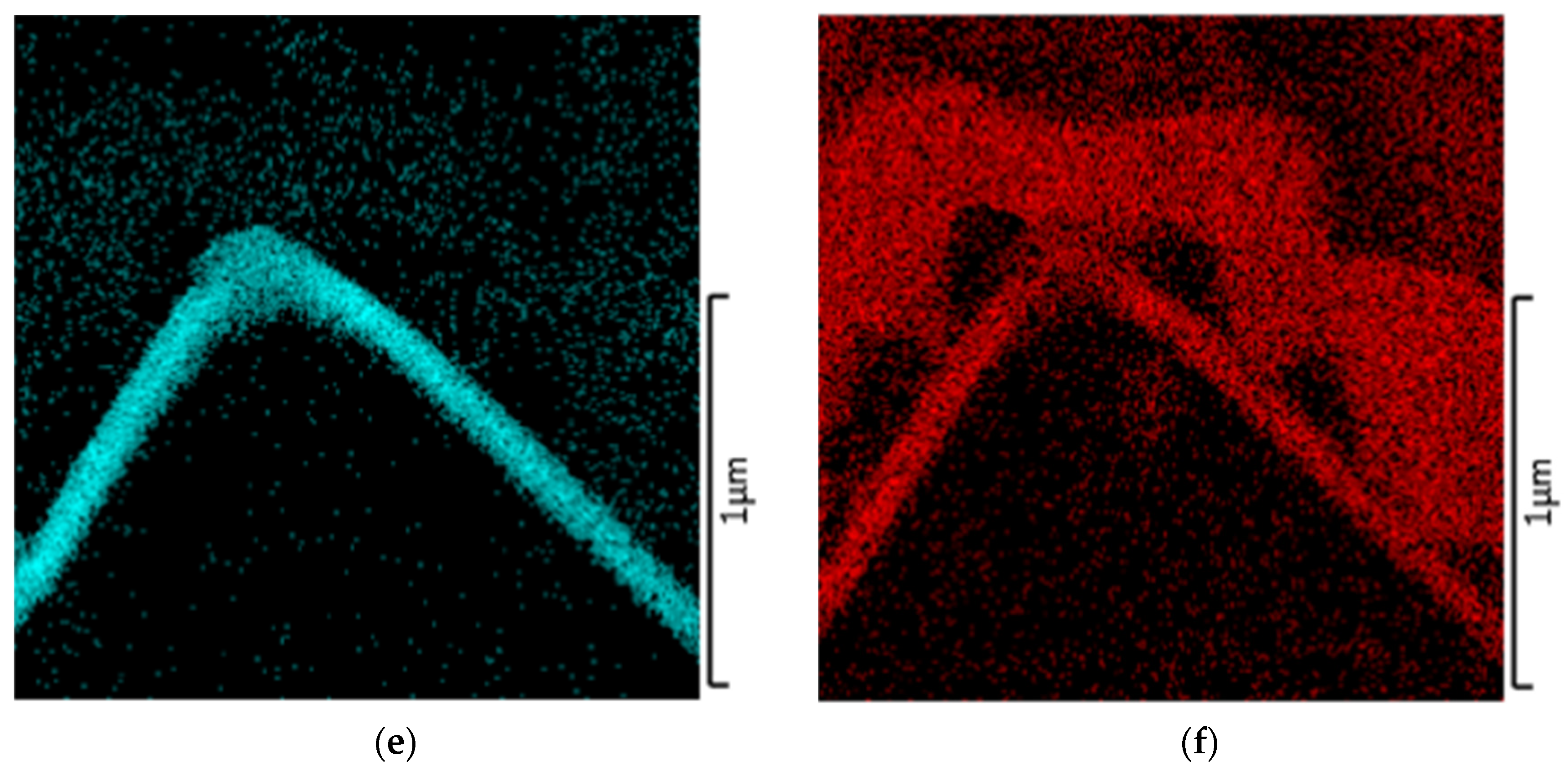
For the annealing of the samples at temperatures of 500, 600, and 700 °C, STEM images also confirm that the copper thin film detached from AZO/Si in the valley of the textured silicon substrate after annealing. Additionally, the gap between the copper and AZO layers increases as temperature increases. For the sample annealed at 800 °C, the TEM and STEM micrographs of Cu/AZO/Si are presented in
Figure 5a,b, respectively. Additionally, the EDS map of Si, Cu, Zn, and O is illustrated in
Figure 5c–f, respectively. The copper layer starts to agglomerate and almost leaves the textured structure’s valley area from
Figure 5. The AZO layer seems stable even after annealing at 800 °C, and the copper element stays above the AZO layer. The copper layer also presents the oxygen signal from
Figure 3f and
Figure 5f. The origin of oxygen migration to the copper layer needs further identification. The STEM-EDS evidence that copper does not diffuse through the AZO layer to the silicon substrate. Therefore, the AZO thin film is also an excellent diffusion barrier layer to prevent copper diffuse into the silicon substrate.
To understand the formation of the gap at the copper and AZO/Si interface, the tape and peel-off tests were used to evaluate copper’s adhesion on the AZO/Si substrate. About 15 µm thick copper layer deposited on the as-deposited Cu/AZO/Si by electroplating for tape and peel-off tests. The sample is designed as E-Cu/Cu/AZO/Si. No copper remained on the AZO/Si after the 180° tape test.
Figure 6 shows the peel force diagram for the E-Cu/Cu/AZO/Si sample. The maximum and average peel force values were 0.39 and 0.2 N/mm, respectively. The results indicated that the adhesion between copper and AZO/Si is weak. It can imply that the adhesion strength will decrease as annealed temperature increases due to the voids emerging when the temperature is higher than 400 °C. Lee also reported a copper seed layer deposited on an indium tin oxide (ITO) by electron-beam evaporation [
14]. After the copper seed layers were deposited, copper/silver (Cu/Ag) metal stacks were plated on the sample using the light-induced plating (LIP) technique. Additionally, adhesive contact between copper and ITO was evaluated by the tape test [
14]. The results show that pure copper was mostly detached from the ITO surface after the tape test. Their results also indicated that the adhesive force between copper and ITO/Si is very weak. Kang deposited the (Ti(30 nm)/Cu(100 nm)) on p-type (1 0 0) Si as a seed layer. Then thick copper was electroplated on the seed layer [
13]. They found that rapid thermal annealing (RTA) caused the electroplated films to fail to adhere to the Si. The adhesion strength of copper and ITO or Si was deficient from Lee’s and Kang’s reports. Our result shows that the adhesion between copper and AZO/Si is very weak, from the tape test. Additionally, the gap formed at the copper and AZO/Si interface easily after high-temperature annealing. It can imply that the copper detached from the AZO/textured silicon after annealing due to the weak adhesion of copper thin films on the AZO/Si. Additionally, the separation of copper and AZO/Si became serious at high-temperature treatments.

