Article

Influence of the Sputtering Technique and Thermal Annealing on YSZ Thin Films for Oxygen Sensing Applications

1
Fraunhofer Institute for Solar Energy Systems, Heidenhofstraße 2, 79110 Freiburg, Germany
2
Institute of Space Systems, University of Stuttgart, Pfaffenwaldring 29, 70569 Stuttgart, Germany
*
Author to whom correspondence should be addressed.
Coatings 2021, 11(10), 1165; https://doi.org/10.3390/coatings11101165
Submission received: 27 July 2021 / Revised: 20 September 2021 / Accepted: 22 September 2021 / Published: 27 September 2021
(This article belongs to the Special Issue Magnetron Sputtering Deposition of Thin Films)

Abstract

:
Yttria-stabilized zirconia (YSZ) thin films were deposited using direct current (reactive and metallic) and radio frequency magnetron sputtering. The effect of the deposition technique and annealing treatment on the microstructure and crystallinity of the thin films was assessed. Using the films produced in this work, oxygen gas sensors were built and their performance under vacuum conditions was evaluated. All the films exhibited a cubic crystalline structure after a post-deposition thermal treatment, regardless of the sputtering technique. When the annealing treatment surpassed 1000 °C, impurities were detected on the thin film surface. The oxygen gas sensors employing the reactive and oxide-sputtered YSZ thin films displayed a proportional increase in the sensor current as the oxygen partial pressure was increased in the evaluated pressure range (5 × 10⁻⁶ to 2 × 10⁻³ mbar). The sensors which employed the metallic-deposited YSZ films suffered from electronic conductivity at low partial pressures.

1. Introduction

Yttria-stabilized zirconia (YSZ) is widely employed in technical applications such as thermal barrier coatings [1,2,3], solid oxide fuel cells (SOFC) [4,5,6,7], and oxygen gas sensors [8,9]. Besides its high thermal and mechanical stability, the ionic conductivity of YSZ plays a major role in most of its applications. Zirconia-based oxygen gas sensors can be employed for monitoring the oxygen content in a gas flow or to optimize combustion processes [8]. With the development of microfabrication technologies in the past decades, miniaturized sensors with low power consumption, high sensitivity, high durability, and quick response time have become the focus of today’s research [10]. Therefore, the deposition of thin films with high ionic conductivity is necessary to meet these requirements.
Different technologies are readily available for the fabrication of YSZ thin films, i.e., sol–gel processes [11,12], chemical vapor deposition (CVD) [6,13], and physical vapor deposition (PVD) [14,15,16]. Magnetron sputtering is a widespread PVD technology used to produce uniform thin layers from a few nanometers up to a few micrometers. Even though high-quality films can be deposited at room temperature, a post-deposition thermal treatment can enhance the ionic conductivity by improving the crystallinity and density of the film [3,5,17,18].
In a typical direct current (DC) sputtering deposition, an electrical conducting target and an inert gas, commonly a metal target and argon, are employed to deposit thin films. If a mixture of an inert and reactive gas (e.g., oxygen) is employed, then a compound material is formed (e.g., oxide). This is also known as reactive sputtering. As the amount of reactive gas is increased, the deposition rate decreases, and the process becomes unstable due to the formation of a compound material on the target surface commonly referred to as “target poisoning”. Therefore, substoichiometric oxides are occasionally deposited through reactive sputtering due to its lower complexity. During this work, reactive sputtering refers to the deposition of substoichiometric oxide films. Meanwhile, radio frequency (RF) sputtering allows the usage of a dielectric material as the target and the deposition of stoichiometric oxide films is possible. RF sputtering has lower deposition rates and higher costs in comparison to DC sputtering.
Since the end of the 1970s, oxygen (lambda) sensors based on a zirconia solid-state electrolyte have been employed to optimize the fuel combustion process on automobiles. Potentiometric sensors such as the lambda sensor measure a voltage between the analyzed gas and the reference gas, typically air, in order to calculate the oxygen concentration [19]. The need of a reference gas hinders the usage of potentiometric sensors “in situ” for vacuum applications. Contrary to the potentiometric principle, amperometric sensors are able to determine the oxygen concentration of gases without the need of a reference gas. By intentionally applying a voltage between the electrodes, a current proportional to the oxygen concentration can be measured [20]. In order to ensure this proportionality, the sensors need to operate under diffusion-limited conditions [8]. This can be achieved by using a porous thin film on top of the sensing electrode which acts as a diffusion barrier.
Götsch et al. deposited YSZ thin films with 3 to 40 mol.% yttria (Y2O3) concentrations through dc ion beam sputtering [21]. The films with an yttria concentration from 8 to 20 mol.% exhibited a cubic crystal structure. Rusli et al. demonstrated that the crystalline structure and morphology of rf-sputtered 8 mol.% yttria-stabilized zirconia (8YSZ) thin films can be tailored through a post-deposition annealing treatment from 380 to 600 °C [22,23]. Smeacetto et al. reported to have deposited 8YSZ thin films of 100 and 200 nm thickness with high ionic conductivity through rf-sputtering for SOFC’s purposes [24].
In this work, DC (reactive and metallic) and RF (oxide) sputtering techniques were used to deposit yttria-stabilized zirconia (YSZ) thin films. The effect of a post-deposition thermal treatment from 600 to 1200 °C on the crystal structure, morphology, and elemental composition of the thin films was evaluated. Finally, the YSZ thin films were used as a solid-state electrolyte in amperometric oxygen gas sensors fabricated by means of a lift-off photolithography process. The gas sensing performance for low oxygen partial pressures under vacuum conditions was investigated using a self-built testing chamber and data acquisition program at the Institute of Space Systems (IRS) of the University of Stuttgart.

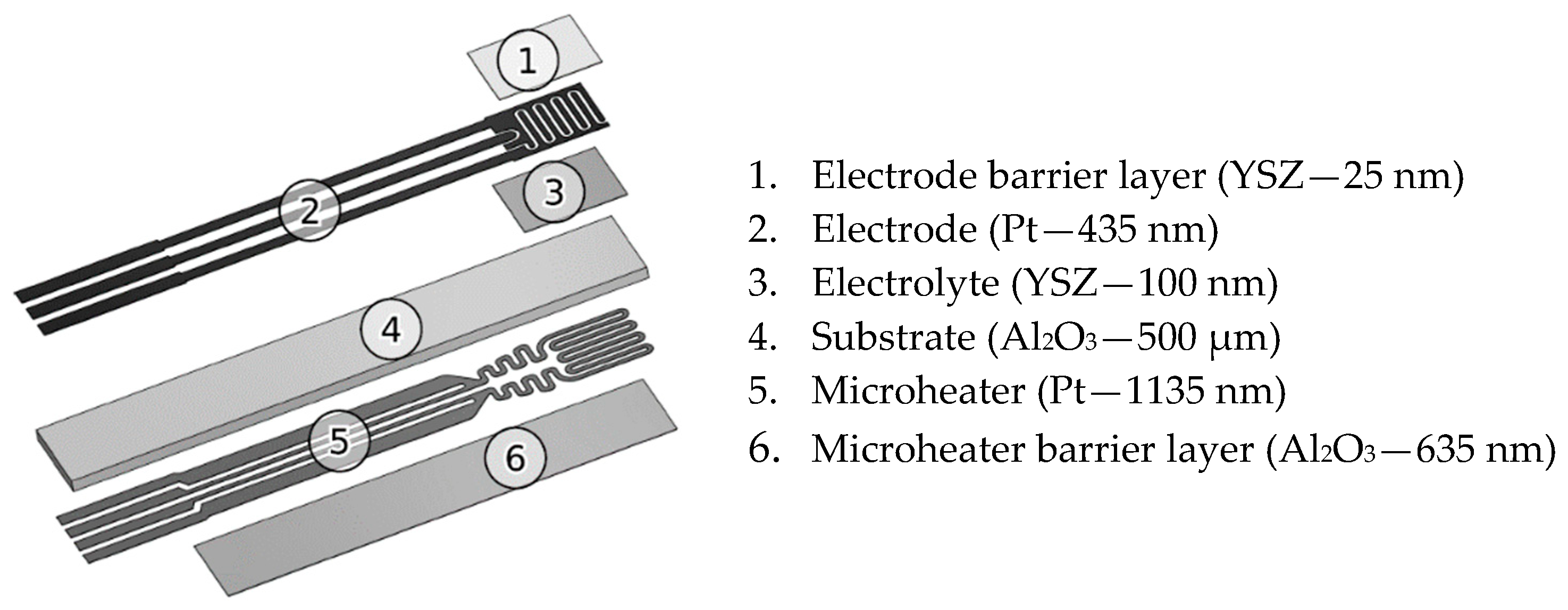
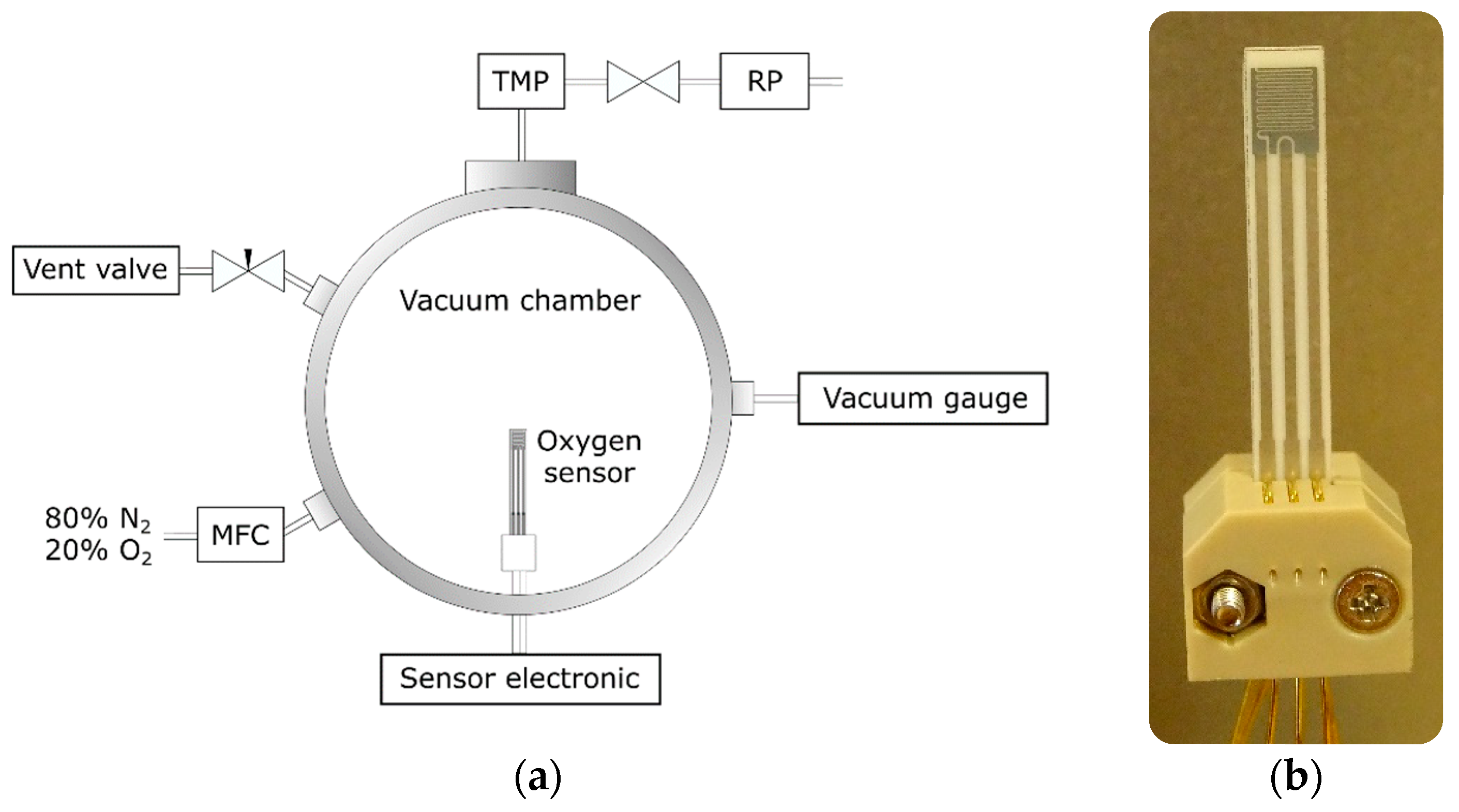
2. Materials and Methods

In this work, 100 nm thin films of yttria-stabilized zirconia (YSZ) were deposited using DC and RF magnetron sputtering at the Fraunhofer Institute for Solar Energy Systems in Freiburg, Germany. Both DC deposition processes, reactive and metallic, were conducted in a custom-made sputtering machine (Interpane E&B, Lauenförde, Germany) using a 80:20 at.% Zr:Y metallic alloy target (99.99% purity) from Sindlhauser Materials. The RF depositions were carried out in an FHR.Star.100-TetraCo sputtering machine (FHR Anlagenbau, Ottendorf-Okrilla, Germany), using a 90:10 mol.% ZrO2:Y2O3 oxide target (99.95% purity). The thin films were sputtered using argon as sputtering gas at a sputtering pressure of about 1.3 × 10⁻³ mbar and a base vacuum pressure of 1 × 10⁻⁵ mbar. For the reactive-sputtered films, an additional oxygen flow was employed. The deposition parameters are shown in Table 1.
The YSZ thin films were then employed as a solid-state electrolyte for fabricating amperometric oxygen sensors. The sensors produced in this work were manufactured completely using thin films deposited via magnetron sputtering. The electrode and the microheater were deposited by (metallic) DC sputtering and their corresponding barrier layers using reactive DC sputtering. Polycrystalline aluminum oxide substrates from Kyocera (model: A493, purity: 99.6%) were used for the sensor fabrication and characterization of the thin films. The thin film patterns were achieved by a lift-off photolithography process using the negative photoresists AZ nLoF 2035 and 2070 (MicroChemicals, Ulm, Germany) and an EVG mask aligner model 6200 MA (EV Group, Sankt Florian am Inn, Austria).
A schematical setup of the YSZ-based O2-sensor is illustrated in Figure 1. The dimensions of a single sensor were 3.5 × 0.5 × 23 mm (width × depth × height). The electrolyte was sputtered and annealed before the deposition of the additional layers. To improve the adhesion between the platinum layers and the Al2O3 substrate, a 10 nm platinum oxide adhesion layer was used between the electrode or the heater and the substrate. Likewise, a barrier layer was deposited on top of both platinum films (electrode and microheater) to avoid the rapid agglomeration of the films and to guarantee the diffusion-limited principle of the amperometric sensor. The YSZ films were deposited only under and above the interdigitated working electrode to avoid short circuits and signal distortion during the sensor operation.
The crystallinity of the films was characterized using grazing incidence X-ray diffraction (GIXD) in a Philips X’Pert MRD system (Malvern Panalytical, Malvern, England) equipped with a CuKα X-ray source. The characterization of the microstructure and chemical composition was examined using a scanning electron microscope (SEM) model FE-SEM S-4700 (Hitachi, Tokyo, Japan) and a Dimension Edge Atomic Force Microscope (AFM) (Bruker, Billerica, MA, USA). The elemental composition was analyzed through X-ray photoelectron spectroscopy (XPS) using a PHI Quantera II (Physical Electronics, Chanhassen, MN, USA). The film thickness was measured using a Dektak 6M profilometer (Veeco Instruments, New York, NY, USA). These characterization techniques were employed on plain YSZ thin films sputtered on pristine alumina substrates, without any further thin films or microstructures.
Due to the potential application of the sensors in space systems and in industrial vacuum coating processes, the characterization was performed under vacuum conditions. The developed oxygen gas sensor prototypes were investigated in a custom-made system shown in Figure 2. The sensors were mounted on a holder made of PEEK polymer, where the sensor is strained using two screws and contacted with gold-coated wires. The PEEK polymer is reported to be thermally stable up to 575 °C [26]. No sign of thermal decomposition during the sensor operation was observed. The data acquisition and sensor operation were accomplished through a home-made electronic system. The test chamber was evacuated to a base pressure of ca. 1 × 10⁻⁷ mbar using the combination of a rotary and a turbomolecular pump models DUO10M/TMU521YP (Pfeiffer Vacuum, Asslar, Germany). The total pressure inside the chamber was measured using a wide-range vacuum gauge model ATMION (JEVATEC, Jena, Germany). Gas flow rates were regulated by a mass flow controller model MF1 Compact (MKS Instruments, Andover, MA, USA). For the sensor characterization presented in this work, after achieving the base pressure of 1 × 10⁻⁷ mbar in the chamber, a flow of synthetic gas (20% O2, 80% N2) was used to achieve the desired total pressure. The oxygen partial pressure ( p O 2 ) was set to be 20% of the total pressure. The sensor current was recorded while varying the oxygen partial pressure every 5 min in a cyclic manner for a total of ca. 45 h. A cycle consisted of 9 increasing and 9 decreasing steps from 5 × 10⁻⁶ to 2 × 10⁻³ mbar. During the characterization, the sensors were heated to ca. 600 °C using the platinum resistance microheater on the back side. The operation of the microheater is described in [25]. This temperature was chosen as a trade-off between the YSZ ionic conductivity and the platinum stability.

3. Results and Discussion
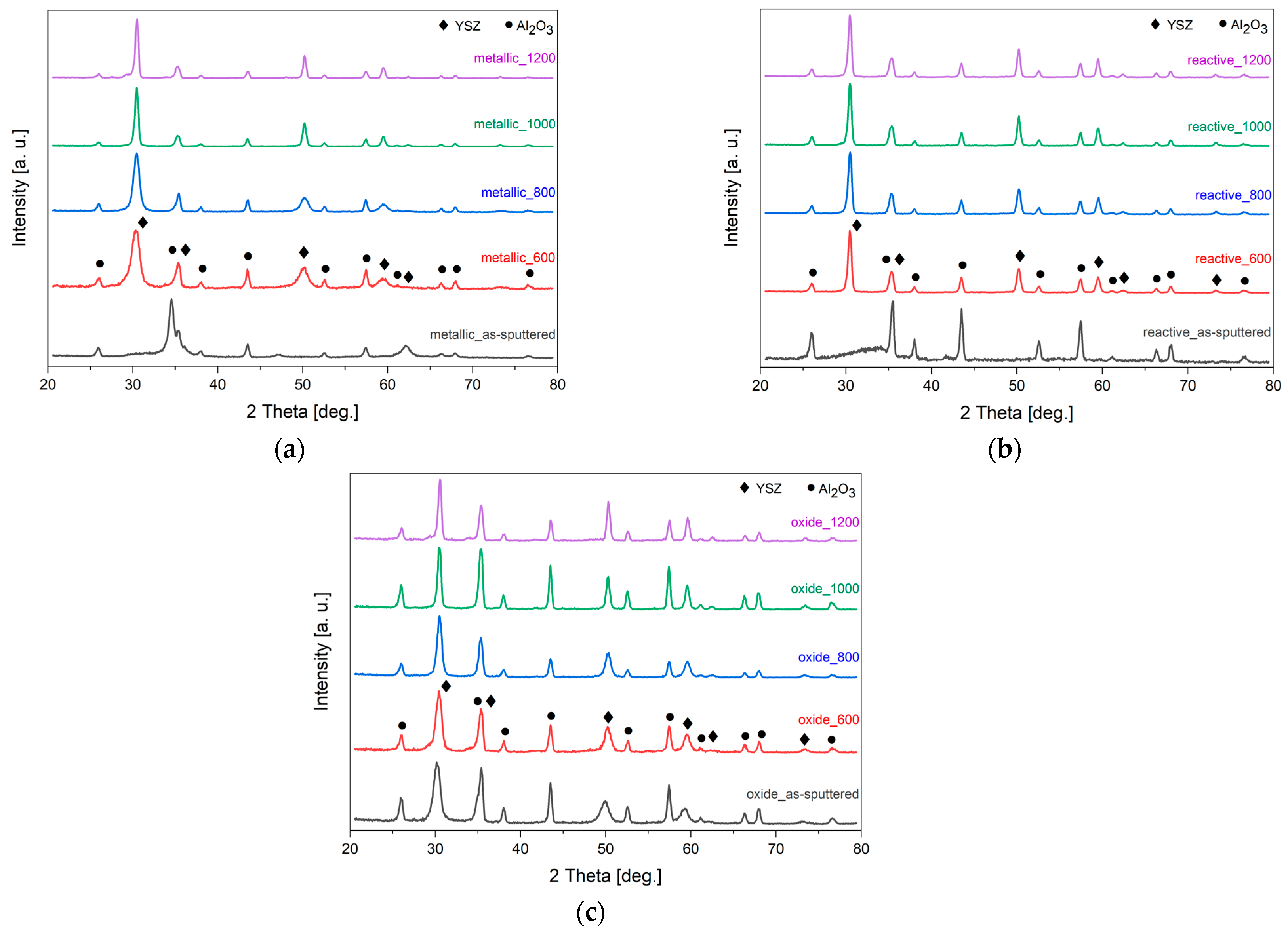
3.1. Crystallinity

The YSZ thin films were deposited at room temperature followed by an annealing process in air for 4 h in a furnace at temperatures ranging from 600 to 1200 °C. The X-ray diffraction of the YSZ films as deposited and after annealing are shown in Figure 3. In Figure 3a,b, the metallic and reactive-sputtered films are amorphous after deposition, only peaks corresponding to the Al2O3 substrate can be observed, and no reflections belonging to the cubic zirconia phase were identified. In Figure 3c, the cubic phase can be observed in the rf-sputtered films directly after deposition. After the heat treatment at 600 °C, all films displayed the desired cubic phase regardless of the deposition technique. The cubic phase was identified using the PDF Card No. 01-082-1246 from the ICDD Database. No other crystal phase was identified, even after high temperature post-deposition treatment.
The grain size of the YSZ thin films was calculated using the Scherrer equation described in [27]:
D m e a n = K λ β c o s θ
where K is the crystallite shape factor (in this work K = 0.94), λ is the X-ray wavelength, β is the full width at half maximum (FWHM) of the (111) reflection located at approximately 2 θ = 30°, and θ is the diffraction angle. The results are summarized in Table 2. The grain size of the DC-metallic and RF-oxide sputtered films increased considerably from approximately 11–13 to 29–32 nm as the annealing temperature was raised from 600 to 1200 °C. Meanwhile, the grain size of the DC-reactive sputtered YSZ films did not change significantly after the heat treatment, i.e., from 27 to 29 nm. After annealing at 1200 °C, the grain sizes of the three different sputtering variations are approximately the same.

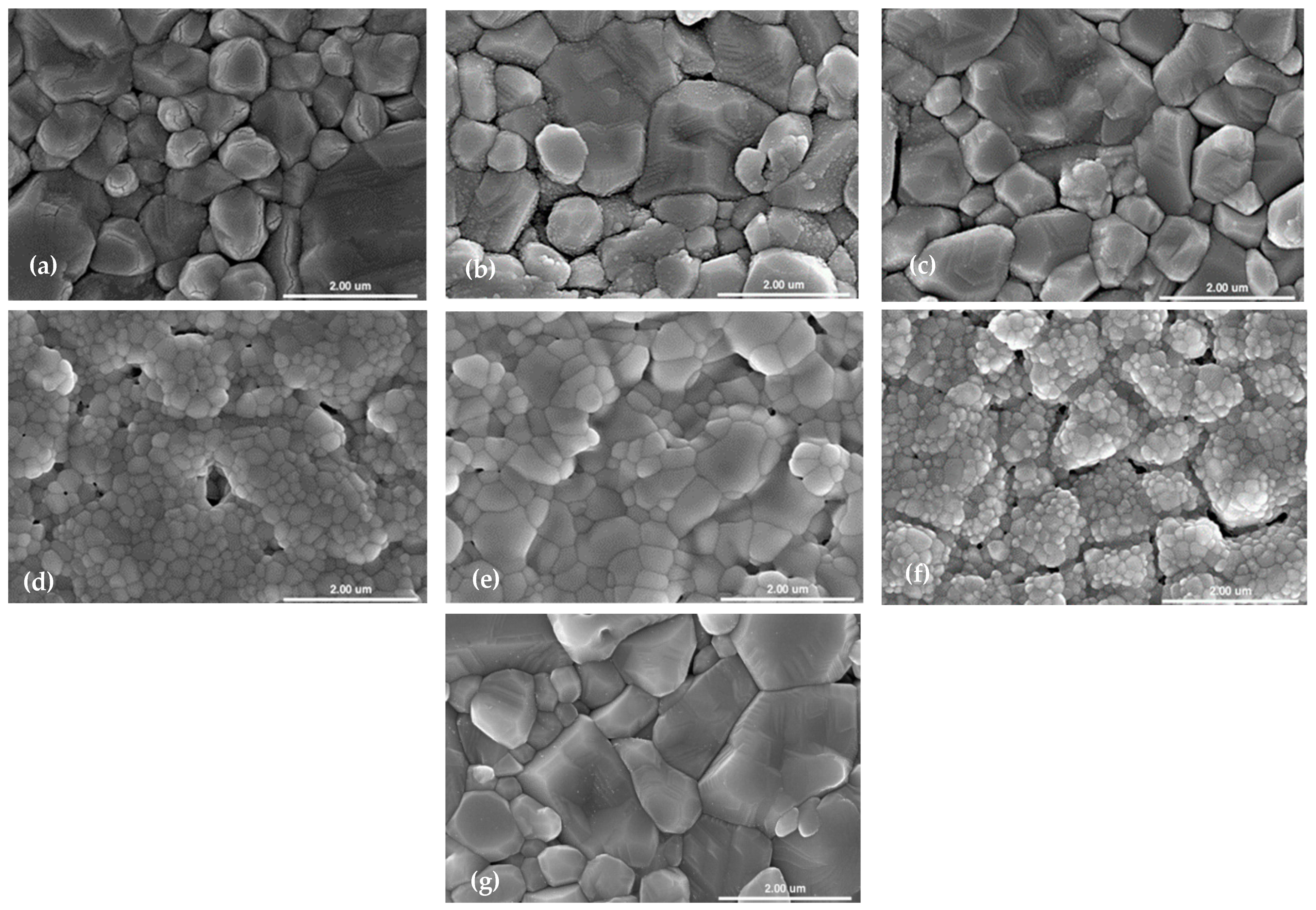
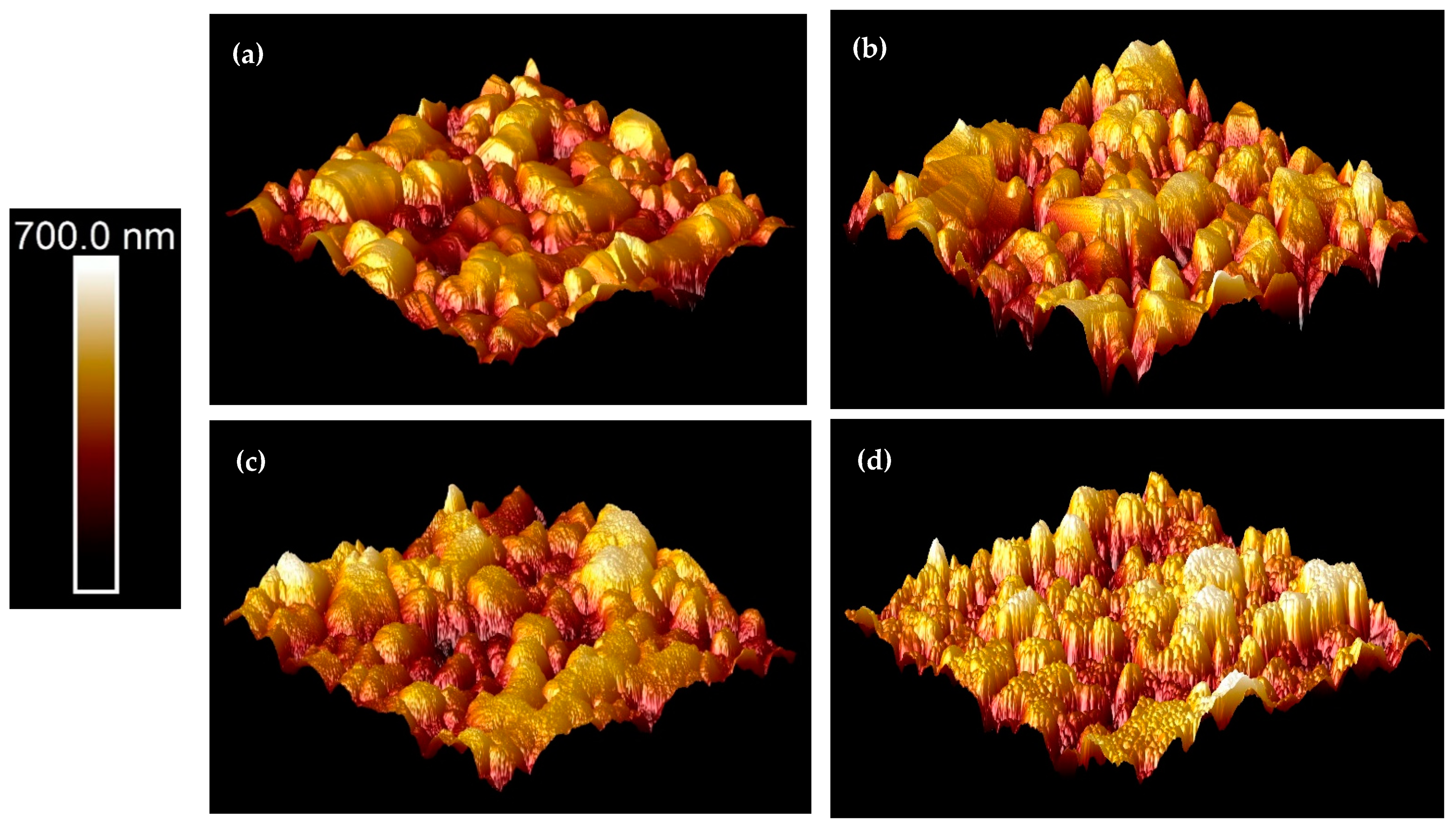
3.2. Thin Film Morphology

In Figure 4, the SEM images of the sputtered films after the annealing treatment at 600 and 1200 °C are shown. At 600 °C, only the large grains of the polycrystalline alumina substrate can be observed. The DC-metallic and DC-reactive YSZ films were subsequently oxidized after deposition by the thermal treatment from their original metallic and substoichiometric oxide condition. In Figure 4a, the DC-metallic film is the only sample with macroscopic cracks after annealing, probably caused by the large volume change and thermal stresses during oxidation. Voids are visible in all samples, especially at the grain boundaries of the substrate.
The surface roughness was analyzed through AFM measurements, and some results are shown in Figure 5. The high surface roughness (Ra = 0.05–0.08 µm, according to the supplier) of the substrate (Figure 5a) hinders a quantitative analysis of the surface roughness evolution as the annealing temperature is raised.
In agreement with the XRD results, it can be noticed from Figure 4 and Figure 5 that at 1000 °C a significant grain growth occurs leading to the formation of small YSZ particles on top of the large Al2O3-substrate grains. After annealing at 1200 °C, grain growth continues, and highly crystalline YSZ films are formed. Nevertheless, the effect of the polycrystalline substrate on the microstructure and grain growth of the YSZ films cannot be neglected.

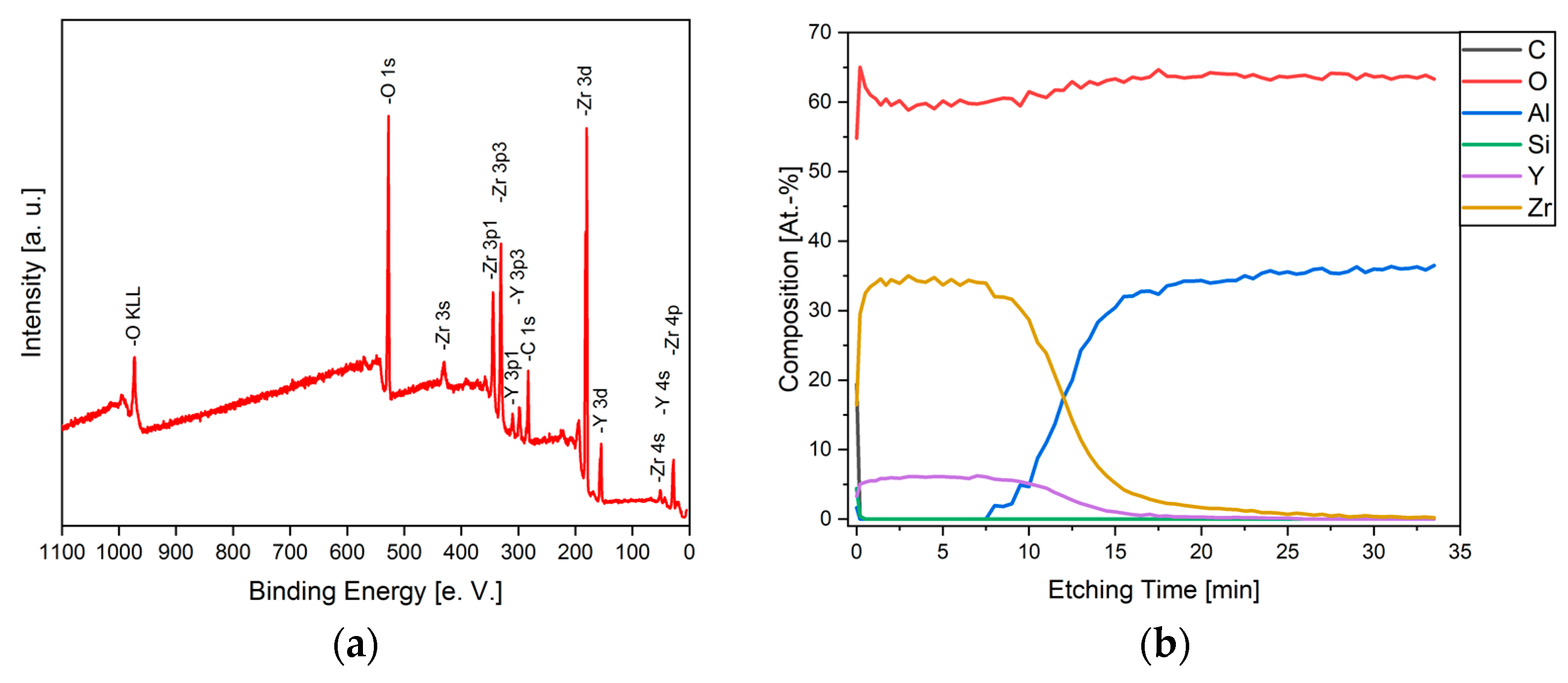
3.3. Elemental Analysis
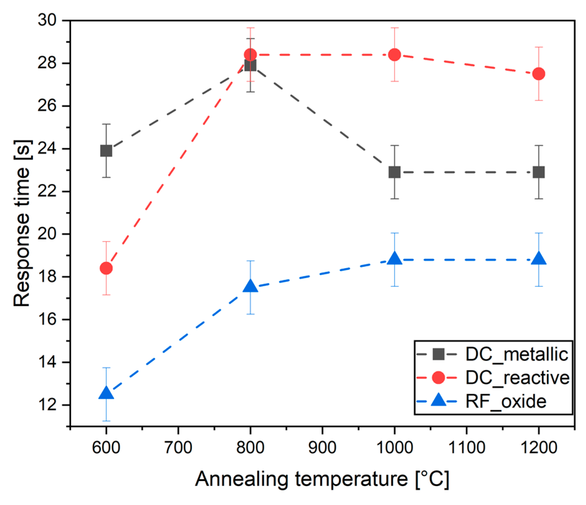
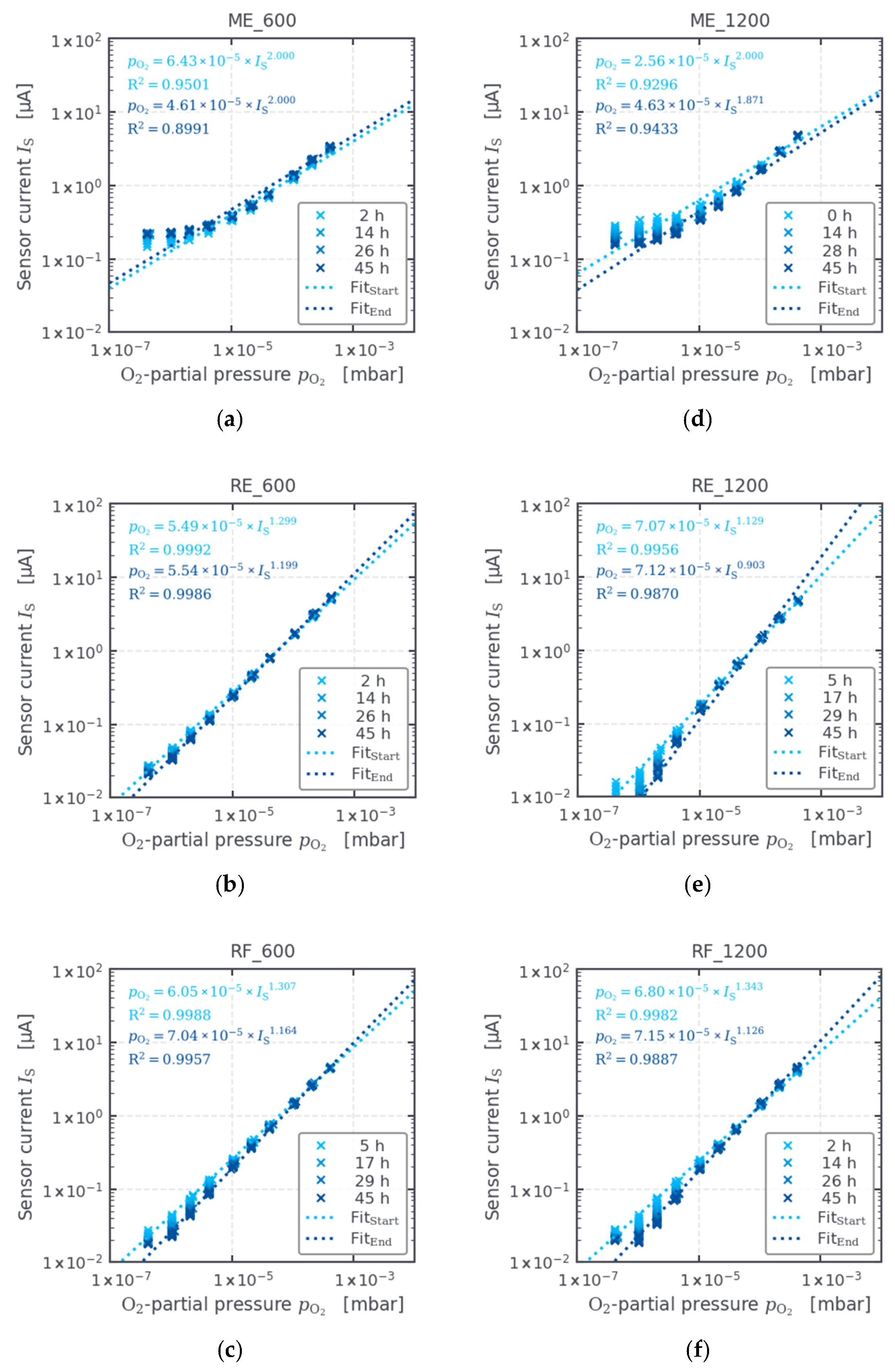
The migration of material impurities is a main concern when annealing at high temperatures. The diffusion of impurities to the surface or into the grain boundaries of the YSZ can deteriorate the ion conductivity of the thin films [28,29]. Likewise, several authors report the segregation of yttria to the film surface [30,31]. Therefore, the RF-oxide deposited samples were analyzed using XPS with depth-profiling to determine the yttria content throughout the thin films and to account for possible impurities.
The XPS surface composition of selected YSZ thin films are summarized in Table 3. The yttria content in mol.% is calculated using the procedure described by Götsch et al. [21]. The yttria content of the films differ depending on the sputtering technique. The surface composition of all films deviated from the desired 10 Y2O3 mol.%. Since the DC-sputtered samples are not fully oxidized after deposition, the surface compositions after annealing at 600 °C were taken as a reference when calculating the Y2O3 content. The samples sputtered with a metallic target (DC-metallic and DC-reactive) presented a higher yttria content than expected, 11.7 and 16.1 at.%, respectively. The yttria surface enrichment could be due to the high mobility of the metallic yttrium atoms during the oxidation process. Additionally, silver cross-contamination (0.3 at.%) was measured in the DC-metallic sample.
On the contrary, the RF-oxide samples deposited from a fully ceramic target displayed a lower but constant yttria surface content, ranging from 8.6 to 9.1 mol.%, despite the heat treatment.
The diffusion of aluminum and silicon to the surface was first detected after annealing the samples at 1000 °C. By increasing the annealing temperature to 1200 °C, the surface diffusion of impurities became more pronounced, reaching a concentration of 1.7 at.% Al and 4.4 at.% Si. In Figure 6, the XPS surface survey spectrum of the rf-sputtered YSZ films before the thermal treatment is shown. The XPS depth-profiling of the RF-sputtered sample after post-annealing at 1200 °C is also shown in Figure 6. Aluminum and silicon atoms were only detected close to the surface, less than 8 nm depth. After etching for 10 min, the alumina substrate is reached.

3.4. Oxygen Sensors

The YSZ films produced by the three different sputtering techniques (DC-metallic, DC-reactive, and RF-oxide) were then used as a solid-state electrolyte in amperometric oxygen sensors and compared according to their oxygen sensing properties. The sensor performances were evaluated by the respective characteristic curves shown in Figure 7. The characteristic curves display the measured current during the increasing p O 2 steps of the cyclic test described previously. The current or signal of the RE_600 and RF_600 sensors increased proportionally with the p O 2 throughout the measured range. The current of the ME_600 sensor at p O 2 < 2 × 10⁻⁴ mbar did not increase significantly. This phenomenon persisted even after annealing at 1200 °C. The lack of sensitivity of the metallic-sputtered sensors could be related to the yttria surface segregation. As stated by Park et al., the yttrium-rich surface obtained after annealing at high temperatures can result in a higher oxygen incorporation barrier and the reduction of the concentration of mobile oxide ion vacancies at the surface [32]. This could be crucial at low partial pressures, where few oxygen molecules reach the sensing electrode. Electronic conduction in the metallic-sputtered YSZ electrolyte could be another possible cause for the low sensitivity at low oxygen partial pressures as suggested by Sridhar [33]. The electronic conductivity could be enhanced by the presence of silver impurities, as found by the XPS analysis. The degradation of the platinum electrode and its effect on the sensor current was not assessed and is out of the scope this work.
An additional parameter to evaluate the sensor performance is the response time. In this work, the response time is defined as the time a sensor needs to achieve 90% of its steady-state current for a defined p O 2 . The sensor was considered to be in a steady state during the last 30 s of a p O 2 increasing step. The response time shown in Figure 8 corresponds to the second cycle and to a p O 2 of 1 × 10⁻⁴ mbar. Even though the sensors using the DC-reactive and RF-oxide sputtered thin films exhibited similar characteristic curves, the RF-oxide sensors displayed the shortest response time. While the response time of the DC-reactive and RF-oxide sensors deteriorate after annealing above 800 °C, the DC-metallic sensors response time improved after thermal annealing at 1000 °C. At this temperature, the largest increase in grain growth occurs as it can be seen in Table 2. This was also confirmed by the AFM grain growth evolution shown in Figure 5. An increase in grain size could lead to fewer grain boundaries, where the ionic conductivity can be lower compared to the bulk [32].
As illustrated by the results which are depicted in Figure 7 and Figure 8, the thermal annealing process at high temperatures (<1000 °C) was detrimental for the sensor performance in most of the cases. Specifically, the response time became slower at low oxygen partial pressures, while a current loss after each cycle was observed in the characteristic curves of the reactive and RF-sputtered films. The surface diffusion of aluminum and silicon atoms on the electrolyte films measured by XPS could explain this. As reported in literature, the segregation of yttrium or impurities to the surface or to the grain boundaries can create a space charge layer (SCL) in which positive charges are accumulated and the oxygen vacancies in the adjacent layers are depleted [34,35,36,37]. Thus, the formation of space charge layers hinders the flow of oxygen ions from grain to grain [38]. This charge build-up can become relevant at low p O 2 , where few oxygen ions flow across the electrolyte.
Nevertheless, annealing can be beneficial for the ionic conductivity of solid-state electrolyte films. Sputtered films suffer from compressive stress due to the ballistic nature of their film growth. As stated by Yeh, thermal annealing in air at 800 °C can improve the ionic conductivity of sputtered YSZ thin films by the relaxation of its residual stress [39]. Similarly, thermal annealing can induce tensile strain, which can enhance the oxygen transport [40]. Therefore, a trade-off between strain relaxation and impurities segregation needs to be achieved when performing a post-deposition thermal treatment on thin films, such as yttria-stabilized zirconia, which are to be used as solid-state electrolyte. Understanding the role of grain boundaries on the ionic transport properties of nanocrystalline materials is of main interest nowadays as solid-state electrolytes become more relevant in applications such as batteries and fuel cells [29,41,42].

4. Conclusions

The feasibility of using magnetron sputtering to manufacture thin film sensors was assessed in this work. Three different sputtering techniques were used to produce YSZ thin films: DC-metallic, DC-reactive, and RF-oxide. The thin films were then annealed in air from 600 to 1200 °C. As the XRD and AFM measurements revealed, after the annealing process at 600 °C, all samples displayed the cubic zirconia phase. After thermal annealing above 1000 °C, defined grains were observed in the SEM and AFM images. The XPS measurements confirmed the diffusion of impurities (Al and Si) to the surface of the RF-sputtered YSZ films after annealing above 1000 °C, whereas yttria surface enrichment was observed in the metallic-sputtered sample after the heat treatment at 600 °C.
The YSZ thin films were used to produce amperometric oxygen sensor prototypes for vacuum applications. Both the DC-reactive and RF-oxide sputtered YSZ films displayed a high correlation between the sensor current and the analyzed oxygen partial pressures. Meanwhile, the metallic-sputtered electrolyte suffered from electronic conduction at low oxygen partial pressures. In general, the sensors manufactured in this work did not display a current stagnation or reach a plateau even at higher oxygen partial pressures ( p O 2 > 1 × 10⁻⁴ mbar). This suggests the presented sensor setup might be also suitable for higher oxygen partial pressures.
By using reactive sputtering to deposit substoichiometric oxides, a higher deposition rate and lower costs can be achieved. Yet, an annealing step is needed to achieve fully oxidized films. Meanwhile, the RF-sputtered fully oxide films exhibited the desired cubic crystal structure directly after deposition. Additionally, the sensors using these films as electrolyte displayed the shortest response time. However, RF-sputtering had the lowest deposition rate between the three techniques assessed in this work. As suggested in the literature, annealing can be beneficial for the oxygen transport properties of the YSZ films. Nevertheless, as shown in this article, high temperatures above 1000 °C may have detrimental effects on the ionic conductivity of the YSZ thin film due to the surface segregation of impurities.

Author Contributions

Conceptualization, supervision, and writing, E.P.A. Data curation and writing, P.G. Investigation and analysis, X.W. Review, project administration, and advice, T.K. and S.F. All authors have read and agreed to the published version of the manuscript.

Funding

This research was funded by the German Federal Ministry for Economic affairs and energy (BMWI) under the joint research project “Oxycontrol”, project number 03ET1519A.

Institutional Review Board Statement

Not applicable.

Informed Consent Statement

Not applicable.

Data Availability Statement

Not applicable.

Acknowledgments

The authors thank Sophie Gledhill and Shankar Bogati for the proofreading and advice for this article. Likewise, the authors thankfully acknowledge Markus Ohnemus for the GIXRD measurements, and Laura Stevens and Oliver Höhn for the AFM measurements.

Conflicts of Interest

The authors declare no conflict of interest.

References

  1. Lange, A.; Braun, R.; Schulz, U. PVD thermal barrier coating systems for Mo–Si–B alloys. Mater. High Temp. 2018, 35, 195–203. [Google Scholar] [CrossRef]
  2. Keyvani, A. Microstructural stability oxidation and hot corrosion resistance of nanostructured Al2O3/YSZ composite compared to conventional YSZ TBC coatings. J. Alloys Compd. 2015, 623, 229–237. [Google Scholar] [CrossRef]
  3. Budinovskii, S.A.; Chubarov, D.A.; Matveev, P.V.; Smirnov, A.A. Deposition and Properties of the Ceramic TBC Layer Prepared by Magnetron Sputtering. Russ. Metall. 2019, 2019, 1280–1284. [Google Scholar] [CrossRef]
  4. Jo, S.; Sharma, B.; Park, D.-H.; Myung, J. Materials and nano-structural processes for use in solid oxide fuel cells: A review. J. Korean Ceram. Soc. 2020, 57, 135–151. [Google Scholar] [CrossRef]
  5. Bae, J.; Chang, I.; Kang, S.; Hong, S.; Cha, S.W.; Kim, Y.B. Post-annealing of thin-film yttria stabilized zirconia electrolytes for anode-supported low-temperature solid oxide fuel cells. J. Nanosci. Nanotechnol. 2014, 14, 9294–9299. [Google Scholar] [CrossRef]
  6. Jang, D.Y.; Kim, H.K.; Kim, J.W.; Bae, K.; Schlupp, M.V.; Park, S.W.; Prestat, M.; Shim, J.H. Low-temperature performance of yttria-stabilized zirconia prepared by atomic layer deposition. J. Power Sources 2015, 274, 611–618. [Google Scholar] [CrossRef]
  7. Nurhamizah, A.R.; Ibrahim, Z.; Muhammad, R.; Wahab, Y.; Sakrani, S. Effect of Annealing Temperature on Platinum/YSZ Thin Film Fabricated Using RF and DC Magnetron Sputtering. In Solid State Phenomena; Trans Tech Publications Ltd.: Stafa-Zurich, Switzerland, 2017; Volume 268, pp. 229–233. [Google Scholar] [CrossRef]
  8. Liu, Y.; Parisi, J.; Sun, X.; Lei, Y. Solid-state gas sensors for high temperature applications—A review. J. Mater. Chem. A 2014, 2, 9919–9943. [Google Scholar] [CrossRef]
  9. Akasaka, S. Thin film YSZ-based limiting current-type oxygen and humidity sensor on thermally oxidized silicon substrates. Sens. Actuators B Chem. 2016, 236, 499–505. [Google Scholar] [CrossRef]
  10. Xu, L.; Dai, Z.; Duan, G.; Guo, L.; Wang, Y.; Zhou, H.; Liu, Y.; Cai, W.; Wang, Y.; Li, T. Micro/Nano gas sensors: A new strategy towards in-situ wafer-level fabrication of high-performance gas sensing chips. Sci. Rep. 2015, 5, 10507. [Google Scholar] [CrossRef] [PubMed] [Green Version]
  11. Butz, B.; Störmer, H.; Gerthsen, D.; Bockmeyer, M.; Krüger, R.; Ivers-Tiffée, E.; Luysberg, M. Microstructure of Nanocrystalline Yttria-Doped Zirconia Thin Films Obtained by Sol-Gel Processing. J. Am. Ceram. Soc. 2008, 91, 2281–2289. [Google Scholar] [CrossRef]
  12. Yamada, T.; Okuda, R.; Hirakoso, H.; Kozuka, H. Sol–gel preparation of yttria-stabilized zirconia thin films and transfer to polycarbonate substrates. J. Sol.-Gel. Sci. Technol. 2019, 92, 554–561. [Google Scholar] [CrossRef]
  13. Schlupp, M.V.F.; Evans, A.; Martynczuk, J.; Prestat, M. Micro-Solid Oxide Fuel Cell Membranes Prepared by Aerosol-Assisted Chemical Vapor Deposition. Adv. Energy Mater. 2014, 4, 1301383. [Google Scholar] [CrossRef]
  14. Solovyev, A. Comparison of Sputter-deposited Single and Multilayer Electrolytes based on Gadolinia-doped Ceria and Yttria- stabilized Zirconia for Solid Oxide Fuel Cells. Int. J. Electrochem. Sci. 2020, 231–240. [Google Scholar] [CrossRef]
  15. Peters, C.; Weber, A.; Butz, B.; Gerthsen, D.; Ivers-Tiffée, E. Grain-Size Effects in YSZ Thin-Film Electrolytes. J. Am. Ceram. Soc. 2009, 92, 2017–2024. [Google Scholar] [CrossRef]
  16. Mengucci, P.; Barucca, G.; Caricato, A.P.; Di Cristoforo, A.; Leggieri, G.; Luches, A.; Majnia, G. Effects of annealing on the microstructure of yttria-stabilised zirconia thin films deposited by laser ablation. Thin Solid Film. 2005, 478, 125–131. [Google Scholar] [CrossRef]
  17. Briois, P.; Gourba, E.; Billard, A.; Ringuedé, A.; Cassir, M. Microstructure—Electrical properties relationship of YSZ thin films reactively sputter-deposited at different pressures. Ionics 2001, 11, 301–305. [Google Scholar] [CrossRef]
  18. Paek, J.Y.; Chang, I.; Park, J.H.; Ji, S.; Cha, S.W. A study on properties of yttrium-stabilized zirconia thin films fabricated by different deposition techniques. Renew. Energy 2014, 65, 202–206. [Google Scholar] [CrossRef]
  19. López-Gándara, C.; Ramos, F.M.; Cirera, A. YSZ-Based Oxygen Sensors and the Use of Nanomaterials: A Review from Classical Models to Current Trends. J. Sens. 2009, 2009, 1–15. [Google Scholar] [CrossRef]
  20. Schwarzwaelder, C. Inkjet Method for the Development of Solid State Electrolyte Sensors for Space Applications; University of Stuttgart: Stuttgart, Germany, 2016. [Google Scholar]
  21. Götsch, T.; Wallisch, W.; Stöger-Pollach, M.; Klötzer, B.; Penner, S. From zirconia to yttria: Sampling the YSZ phase diagram using sputter-deposited thin films. AIP Adv. 2016, 6, 25119. [Google Scholar] [CrossRef] [Green Version]
  22. Rusli, N.A.; Muhammad, R.; Ghoshal, S.K.; Nur, H.; Nayan, N. Annealing temperature induced improved crystallinity of YSZ thin film. Mater. Res. Express 2020, 7, 56406. [Google Scholar] [CrossRef]
  23. Rusli, N.A.; Muhammad, R.; Ghoshal, S.K.; Nur, H.; Nayan, N.; Jaafar, S.N. Bias voltage dependent structure and morphology evolution of magnetron sputtered YSZ thin film: A basic insight. Mater. Res. Express 2019, 6, 106414. [Google Scholar] [CrossRef]
  24. Smeacetto, F.; Salvo, M.; Ajitdoss, L.C.; Perero, S.; Moskalewicz, T.; Boldrini, S.; Doubova, L.; Ferraris, M. Yttria-stabilized zirconia thin film electrolyte produced by RF sputtering for solid oxide fuel cell applications. Mater. Lett. 2010, 64, 2450–2453. [Google Scholar] [CrossRef]
  25. Kastelik, R. Messsysteme für Sauerstoff-Sensoren auf Basis von Festkörperelektrolyten; University of Stuttgart: Stuttgart, Germany, 2020. [Google Scholar]
  26. Patel, P.; Hull, T.R.; McCabe, R.W.; Flath, D.; Grasmeder, J.; Percy, M. Mechanism of thermal decomposition of poly(ether ether ketone) (PEEK) from a review of decomposition studies. Polym. Degrad. Stab. 2010, 95, 709–718. [Google Scholar] [CrossRef] [Green Version]
  27. Zhang, J.; Huang, X.; Zhang, H.; Xue, Q.; Xu, H.; Wang, L.; Feng, Z. The effect of powder grain size on the microstructure and electrical properties of 8 mol% Y2O3 -stabilized ZrO2. RSC Adv. 2017, 7, 39153–39159. [Google Scholar] [CrossRef] [Green Version]
  28. Subramaniam, K.M.; Rajeswara Rao, L.L.; Jampana, N. Investigation of Annealing Induced Yttria Segregation in Sputtered Yttria-Stabilized Zirconia Thin Films. J. Am. Ceram. Soc. 2015, 98, 3389–3397. [Google Scholar] [CrossRef]
  29. An, J.; Bae, J.; Hong, S.; Koo, B.; Kim, Y.-B.; Gür, T.M.; Prinz, F.B. Grain boundary blocking of ionic conductivity in nanocrystalline yttria-doped ceria thin films. Scr. Mater. 2015, 104, 45–48. [Google Scholar] [CrossRef] [Green Version]
  30. Vonk, V.; Khorshidi, N.; Stierle, A.; Dosch, H. Atomic structure and composition of the yttria-stabilized zirconia (111) surface. Surf. Sci. 2013, 612, 69–76. [Google Scholar] [CrossRef]
  31. Ridder, M.D.; Welzenis, R.G.V.; Gon, A.W.D.V.D.; Brongersma, H.H.; Wulff, S.; Chu, W.-F.; Weppner, W. Subsurface segregation of yttria in yttria stabilized zirconia. J. Appl. Phys. 2002, 92, 3056–3064. [Google Scholar] [CrossRef] [Green Version]
  32. Park, J.S.; An, J.; Lee, M.H.; Fritz, B.P.; Lee, W. Effects of surface chemistry and microstructure of electrolyte on oxygen reduction kinetics of solid oxide fuel cells. J. Power Sources 2015, 295, 74–78. [Google Scholar] [CrossRef]
  33. Sridhar, K.; Blanchard, J. Electronic conduction in low oxygen partial pressure measurements using an amperometric zirconia oxygen sensor. Sens. Actuators B 1999, 59, 60–67. [Google Scholar] [CrossRef]
  34. Durá, O.J.; La López de Torre, M.A.; Vázquez, L.; Chaboy, J.; Boada, R.; Rivera-Calzada, A.; Santamaria, J.; Leon, C. Ionic conductivity of nanocrystalline yttria-stabilized zirconia: Grain boundary and size effects. Phys. Rev. B 2010, 81. [Google Scholar] [CrossRef] [Green Version]
  35. Guo, X.; Maier, J. Grain Boundary Blocking Effect in Zirconia: A Schottky Barrier Analysis. J. Electrochem. Soc. 2001, 148, E121–E126. [Google Scholar] [CrossRef]
  36. Guo, X.; Waser, R. Electrical properties of the grain boundaries of oxygen ion conductors: Acceptor-doped zirconia and ceria. Prog. Mater. Sci. 2006, 51, 151–210. [Google Scholar] [CrossRef]
  37. Lee, H.B.; Prinz, F.B.; Cai, W. Atomistic simulations of grain boundary segregation in nanocrystalline yttria-stabilized zirconia and gadolinia-doped ceria solid oxide electrolytes. Acta Mater. 2013, 61, 3872–3887. [Google Scholar] [CrossRef]
  38. Schlupp, M.V.F.; Scherrer, B.; Ma, H.; Grolig, J.G.; Martynczuk, J.; Prestat, M.; Gauckler, L.J. Influence of microstructure on the cross-plane oxygen ion conductivity of yttria stabilized zirconia thin films. Phys. Status Solidi A 2012, 209, 1414–1422. [Google Scholar] [CrossRef]
  39. Yeh, T.-H.; Lin, R.-D.; Cherng, J.-S. Significantly enhanced ionic conductivity of yttria-stabilized zirconia polycrystalline nano-film by thermal annealing. Thin Solid Film 2013, 544, 148–151. [Google Scholar] [CrossRef]
  40. Mills, E.M.; Kleine-Boymann, M.; Janek, J.; Yang, H.; Browning, N.D.; Takamura, Y.; Kim, S. YSZ thin films with minimized grain boundary resistivity. Phys. Chem. Chem. Phys. 2016, 18, 10486–10491. [Google Scholar] [CrossRef] [PubMed] [Green Version]
  41. Guo, X.; Sigle, W.; Maier, J. Blocking Grain Boundaries in Yttria-Doped and Undoped Ceria Ceramics of High Purity. J. Am. Ceram. Soc. 2003, 86, 77–87. [Google Scholar] [CrossRef]
  42. Bae, J.W.; Park, J.Y.; Hwang, S.W.; Yeom, G.Y.; Kim, K.D.; Cho, Y.A.; Jeon, J.S.; Choi, D. Characterization of Yttria-Stabilized Zirconia Thin Films Prepared by Radio Frequency Magnetron Sputtering for a Combustion Control Oxygen Sensor. J. Electrochem. Soc. 2000, 147, 2380–2384. [Google Scholar] [CrossRef] [Green Version]
Figure 1. Schematic sensor setup and film thickness, adapted from [25].
Coatings 11 01165 g001
Figure 2. (a) Schematic diagram of the vacuum chamber for sensor characterization; (b) sensor mounted on the PEEK-adapter and contacted with the gold-coated wires.
Coatings 11 01165 g002
Figure 3. GIXRD of the sputtered 10YSZ films before and after the annealing treatment: (a) dc-metallic; (b) dc-reactive; and (c) rf-oxide. The reflections belonging to the Al2O3 substrate and the YSZ are marked by (●) and (♦), respectively.
Coatings 11 01165 g003
Figure 4. SEM images of the sputtered YSZ films after the thermal annealing process at 600 (above) and 1200 °C (below): (a,d) DC-metallic; (b,e) DC-reactive; and (c,f) RF-oxide. In (g) the pristine Al2O3 polycrystalline substrate is shown for comparison.
Coatings 11 01165 g004
Figure 5. Surface roughness evolution measured by AFM: of the (a) Al2O3 substrate; (b) RF_800; (c) RF_1000; and (d) RF_1200 samples. The color scale on the left side represents the surface height.
Coatings 11 01165 g005
Figure 6. (a) XPS surface survey of the RF-oxide_as-sputtered sample and (b) depth-profile of the RF-oxide_1200.
Coatings 11 01165 g006
Figure 7. Characteristic curves of the sensors manufactured using the YSZ thin films as solid-state electrolyte after the thermal annealing treatment at 600 and 1200 °C: (a,d) DC-metallic; (b,e) DC-reactive; and (c,f) RF-oxide. The Y-axes are presented in logarithmic scale. The current drift over the time is represented by the (blue) color scale.
Coatings 11 01165 g007
Figure 8. Sensor response time at a p O 2 = 1 × 10⁻⁴ mbar using the annealed YSZ thin films as solid-state electrolyte.
Coatings 11 01165 g008
Table 1. Sputtering deposition parameters.
Power SourceModeSputtering Power Density (w/cm2)Ar Flow (sscm)O2 Flow (sscm)
direct currentmetallic1.27580
direct currentreactive2.085815
radio frequencyoxide5.09280
Table 2. Calculated grain size in nm using the Scherrer equation and the (111) reflection.
600 °C800 °C1000 °C1200 °C
DC-metallic11132632
DC-reactive27262929
RF-oxide13182729
Table 3. XPS surface survey of selected YSZ thin films. The concentration is expressed in at.%, unless otherwise stated.
SampleCOAlSiAgZrYY2O3 (mol.%)
DC-reactive_60019.954.900020.05.311.7
DC-metallic_60022.652.7000.317.76.816.1
RF-oxide_as-sputtered26.151.000019.23.78.8
RF-oxide_60022.452.900020.73.98.6
RF-oxide_80038.942.000015.53.08.8
RF-oxide_100021.953.91.11.8017.63.48.8
RF-oxide_120019.454.81.74.4016.43.39.1
Publisher’s Note: MDPI stays neutral with regard to jurisdictional claims in published maps and institutional affiliations.

