Article

Providing a Specified Level of Electromagnetic Shielding with Nickel Thin Films Formed by DC Magnetron Sputtering

by
Oleg A. Testov
1,
Andrey E. Komlev
2,
Kamil G. Gareev
1,3,*,
Ivan K. Khmelnitskiy
1,3,
Victor V. Luchinin
1,3,
Eugeniy N. Sevost’yanov
1 and
Igor O. Testov
1,3
1
Engineering Centre for Microtechnology and Diagnostics, Saint Petersburg Electrotechnical University “LETI”, 197376 Saint Petersburg, Russia
2
Department of Physical Electronics and Technology, Saint Petersburg Electrotechnical University “LETI”, 197376 Saint Petersburg, Russia
3
Department of Micro and Nanoelectronics, Saint Petersburg Electrotechnical University “LETI”, 197376 Saint Petersburg, Russia
*
Author to whom correspondence should be addressed.
Coatings 2021, 11(12), 1455; https://doi.org/10.3390/coatings11121455
Submission received: 4 October 2021 / Revised: 7 November 2021 / Accepted: 25 November 2021 / Published: 26 November 2021
(This article belongs to the Special Issue Magnetron Sputtering Deposition of Thin Films)

Abstract

:
Nickel films of 4–250 nm thickness were produced by DC magnetron sputtering onto glass and silicon substrates. The electrical properties of the films were investigated by the four-probe method and the surface morphology of the films was studied by atomic force microscopy. To measure the shielding effectiveness, a portable closed stand based on horn antennas was used. A theoretical assessment of the shielding effectiveness of nickel films of various thickness under electromagnetic radiation of a range of frequencies was carried out using two different approximations. The results demonstrate the shielding effectiveness of up to 35 dB of the nickel thin films in the frequency range of 2–18 GHz.

Graphical Abstract

1. Introduction

The widespread use of devices generating electromagnetic radiation (EMR) requires operative decisions focused on eliminating related technical problems. First of all, these are the problems of electromagnetic compatibility of various electrical appliances and their protection from an external electromagnetic influence [1]. The main source of electromagnetic waves (EMW) are electronic devices operating in the decimeter (ultra high frequency, 0.3–3.0 GHz) and centimeter (super high frequency, 3–30 GHz) wavelength ranges. There is a trend of increasing operating frequencies of EMW, which aims at increasing the data transfer rate.
The traditional way of preventing the EMW pollution is the use of electromagnetic shields based on high-conductivity metals [2,3], composite materials with conductive [4,5] or magnetic fillers [6,7], conductive polymers [5,8] and other materials [9,10,11] forming a protective shell.
The priority task at the stage of developing an electromagnetic shield is to maximize the value of shielding effectiveness (SE). It is necessary to take into account additional requirements for the shield operational characteristics, such as weight, dimensions and temperature range of operation. Most of the recent solutions in the design of electromagnetic shields are based on high-conductivity metals with the electrical resistivity of ρv < 10.0 μΩ·cm at room temperature [12,13,14].
In addition to high conductivity, a metal coating must have corrosion resistance, high adhesion and minimal internal mechanical stress. The corrosion resistance depends on the properties of the oxide film formed on the metal surface. The protective effect of the oxide film is assessed by its continuity, which is characterized by the ratio of the molecular volume of the compound Vox formed during metal oxidation and the volume of the metal Vm spent on the formation of the molecule of this compound. According to the Pilling–Bedworth ratio, the formation of a continuous oxide film occurs when Vox/Vm ≥ 1. Films with Vox/Vm > 2 can be mechanically unstable, and films with 1 < Vox/Vm < 2 provide a protecting effect against further surface oxidation [15,16,17,18].
The growth of an oxide film can be accompanied by the appearance of various types of internal stresses, such as:
  • Compressive stresses appearing with an increase of the volume of the oxide film (Vox/Vm ˃ 1);
  • Compressive stresses arising in the oxide film growing on a rough surface and causing tearing forces;
  • Stresses arising due to different values of the expansion coefficients of the metal and the oxide film [18].
The values of the coefficients of linear expansion of the metal and the oxide film formed on its surface are given in [18,19,20,21].
After selecting the type of metal that meets the requirements above and additional ones, corresponding to the specific task, it is necessary to determine the metallization thickness, l, providing the specified SE values.
SE can be represented as the ratio of the amplitude of the EMW falling on a unit surface of the shield to the amplitude of the EMW that passed through the shield [22].
The amplitude of the EMW decreases as it penetrates into the conducting medium. The penetration depth, δ, at where the EMW amplitude decreases by a factor of e and its phase shifts by π/2, is called the skin depth. The δ value is calculated by the following equation [1]:
δ = ρ v π f μ 0 μ ,
where f is the frequency of the EMW, µ0 = 4π × 10−7 H·m−1 is the magnetic constant (permeability of vacuum), µ is the relative magnetic permeability of the medium, ρv is the electrical resistivity.
Bulk chemically pure non-magnetic metals, in the absence of external influencing factors, are characterized by constant values of ρv and µ. Therefore, under these conditions, the skin depth is a function of the frequency. When evaluating the value of δ for magnetic metals, it is necessary to take into account the value of µ, which approaches 1 as the frequency increases. Traditionally, the thickness of the electromagnetic shield is chosen in such a way that the condition l > δ is obeyed [1], which predetermines the use of a bulk material instead of a thin film. The weight and size characteristics of an electromagnetic shield can be improved by using thin films and coatings, in particular, of ultrathin (0.1–10.0 nm) and nanometer (10–100 nm) thickness [23].
A metal thin film can be formed on a given surface by various physical or chemical deposition methods. The film formation method should ensure:
  • The possibility of film deposition at a sufficiently low (below melting point) substrate temperature;
  • High adhesion rate of a thin film to the substrate;
  • The growth rate of the film, allowing deposition of layers up to submicron thicknesses in a minimum time interval;
  • Uniformity of thickness on plane substrates with an area of up to several square millimeters;
  • Absence of impurities and droplet phase;
  • Uniformity of the film over its thickness.
The methods of vacuum metallization [24] and, in particular, the magnetron sputtering [6] are quite universal and satisfy the requirements.
The possibility of using a thin film for electromagnetic shielding is associated with the need to solve a rather laborious task—to assess the SE level that it provides. Such an assessment should be carried out taking into account the change in ρv with a change in the thickness of the film and the dependence of magnetic permeability on the frequency of EMW for magnetic materials.
This study is aimed at demonstrating of the possibility of determination of the SE level provided by nickel thin films in the frequency range of 2–18 GHz. In this work, samples of nickel thin films were produced by physical vapor deposition from the gas phase (magnetron sputtering). Their thickness, electrical resistivity, and frequency dependencies of SE were investigated. A comparison of the experimentally obtained SE values with the SE values calculated on the basis of two different approximations was carried out.

2. Materials and Methods

Nickel thin films of various thickness were produced using UVMN-3/320 customized industrial magnetron sputtering set-up (“MIT” Ltd., Saint Petersburg, Russia), designed for Saint Petersburg Electrotechnical University “LETI” (ETU “LETI”), by DC magnetron sputtering on silicon substrates (to study thickness and surface roughness of the films) and glass (to study electrical resistivity and shielding effectiveness of the films). For the manufacture of targets with dimensions of 290 mm × 120 mm and a thickness of 1.5 mm, pure nickel (no more than 0.2 wt.% of impurities) was used.
The use of a thin target allows the magnetic system of the sputtering setup to put nickel to magnetic saturation, in which the magnetic field lines extend beyond the target surface, creating thereby the conditions necessary for the occurrence of a magnetron discharge. The residual pressure in the chamber did not exceed 2 × 10⁻⁴ Pa. An improvement in the adhesion of metal films was achieved through ionic cleaning of the substrate surface in a glow discharge. High-purity argon (volume fraction no less than 99.993%) was used as a plasma-forming gas. The target was sputtered at a constant current at a power of 1.1 kW (current density was 7.2 mA·cm−2) and an argon pressure of 0.1 Pa. The minimum distance from the substrate to the sputtering target was 80 mm. The thickness uniformity of the deposited films over the area was ensured by the orbital rotation of the substrates.
Atomic force microscopy (AFM) with the Veeco Dimension 3100 scanning probe microscope (Veeco Instruments Inc., Plainview, NY, USA) was used to study the thickness and surface of thin films deposited on silicon substrates. The microscope allows scanning surface areas in a range from 500 nm × 500 nm to 60 μm × 60 μm in the XY plane and detect objects in the range of 1–500 nm in the Z direction. The resolution in this study was 20 nm in the XY plane and 0.1 nm in the Z direction. To determine the thickness of the films, the stepped-type structure was formed by covering a part of the substrate surface with a rigidly mechanically fixed piece of a silicon wafer. The Z-profiles of the samples were measured ten times, followed by arithmetic averaging of the height difference along the “step”.
The values of the electrical resistivity of the thin film were measured by the four-probe method using OA3201 digital ohmmeter (JSC NIIEMP, Penza, Russia). The device provides measurement range of 10−5–107 Ω with the maximum nominal permissible error not more than ±0.5% for the full measuring range. Therefore, the final data uncertainty of the four-probe method can be attributed presumably to the thickness estimation and does not exceed ±10%. Metal probes were located along a line, perpendicular to the film surface on equal distances from each other S1 = S2 = S3 = S. Electric current I14 = I passing through Probes 1 and 4, as well as the potential difference between Probes 2 and 3 U23 = U were measured [25,26].
The evaluation of the EMR shielding effectiveness was carried out on the basis of results obtained using a portable closed measuring stand [27,28,29,30,31]. The measurement scheme is shown in Figure 1. This type of stands allows laboratory studies of the effectiveness of EMR shielding by various materials without using expensive anechoic chambers to be carried out.
The principle of operation of the stand [32] is based on the generation and detection of electromagnetic energy by a ZVB-20 vector network analyzer (Rhode and Schwarz, Munich, Germany), to which the P6-124 measuring horn antennas (CJSC SKARD-Electronics, Kursk, Russia) with an operating frequency range of 2.0–18.0 GHz are connected. A test sample with the dimensions of at least 170 × 170 mm is installed in the gap between the horn antennas (Figure 1). The measurement accuracy is mostly affected by the accuracy of the thickness determination of the layer and can be estimated as ±10%.

3. Results and Discussion

3.1. Frequency Dependencies of Magnetic Permeability and Skin Depth

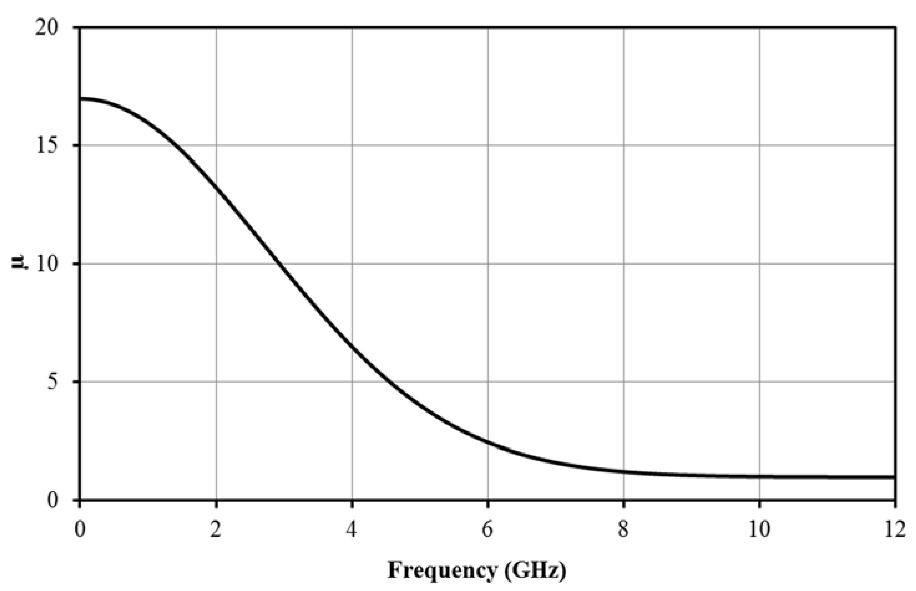
Figure 2 shows the frequency dependence of the relative magnetic permeability of nickel, calculated using the empirical equation [33], based on the averaging nickel µ values determined experimentally [34,35,36,37,38]:
μ = 1 + 16 e x p ( f 2 15 )
where f is the frequency of the EMW.
The choice of equations for the SE calculation depends on the ratio of the l and δ. Based on the calculated nickel µ values and Equation (1) for the bulk material, the values of δ were obtained (Figure 3). For calculations, the values of the electrical resistivity of chemically pure nickel given in [12] were used.
The dependence shown in Figure 3 demonstrates that the condition l < δ is satisfied for the thickness of the nickel coating < 1 μm in the entire experimental frequency range. The specified condition will be used in Section 3.4 for the calculation of SE values.

3.2. Surface Morphology

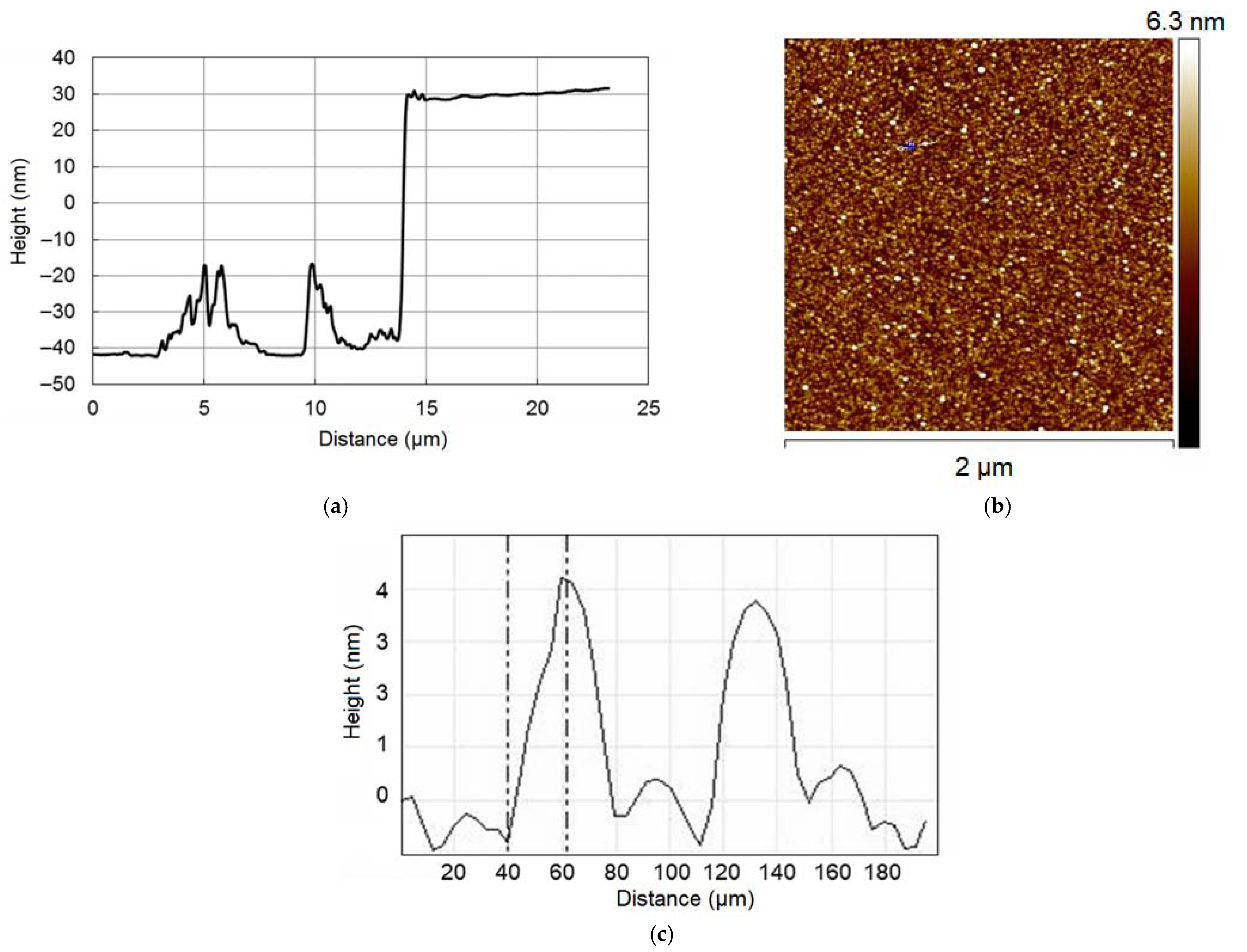
The thicknesses of the produced nickel thin films are shown in Table 1. Determination of the thickness, the surface type and the microrelief height of a thin film sample with a thickness of 70 nm are shown in Figure 4.

3.3. Electrical Resistivity

Taking into account the data from Table 1, the values of the electrical resistivity, ρv, were determined for each sample of a nickel film with a thickness of l << S [25,26]:
ρ v = U I π l n 2 l 4.53 U I l = 4.53 ρ s l ,
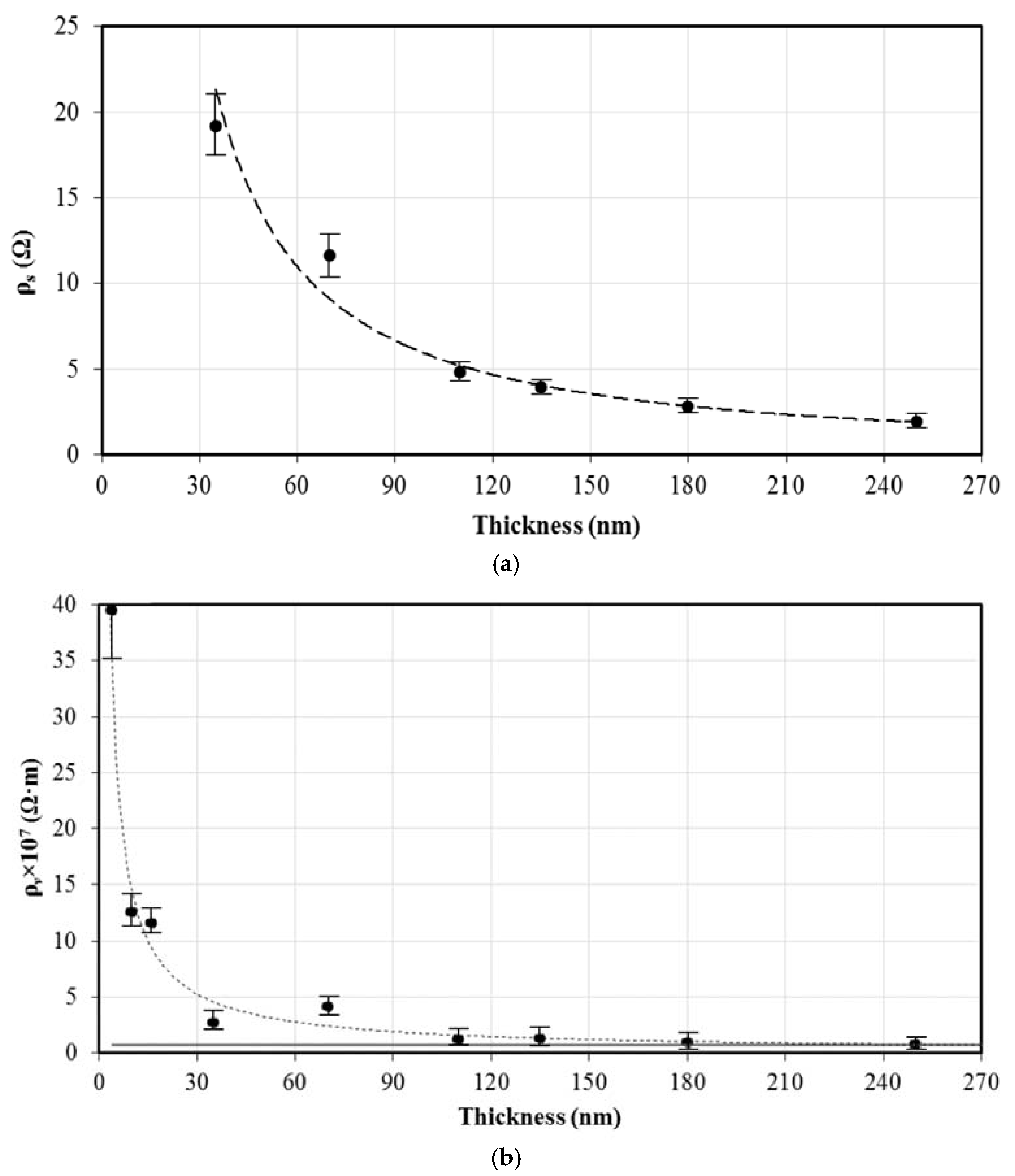
where ρs is the sheet resistance, Ω; l is the film thickness, U is the potential difference between probes; I is the electric current passing through probes. The results are shown in Figure 5.
The character of the dependence shown in Figure 5b implies that at a nickel film thickness of ~100 nm and more, the value of ρv almost does not change, which indicates that it corresponds to the characteristic of a bulk material.
It should be noted that an oxide layer is formed on the metal surface upon contact with oxygen. Oxide films on the metal surface are formed rather quickly even under normal conditions at room temperature. Over time, the growth rate of the oxide film decreases. It is practically impossible to completely eliminate the influence of the corrosion process on the change in the properties of metal thin films over time. Under real conditions, it is necessary to use protective coatings to prevent oxidation of the metal surface and corresponding change of the conductive layer thickness, resulting in a change of film parameters.

3.4. Electromagnetic Shielding Effectiveness

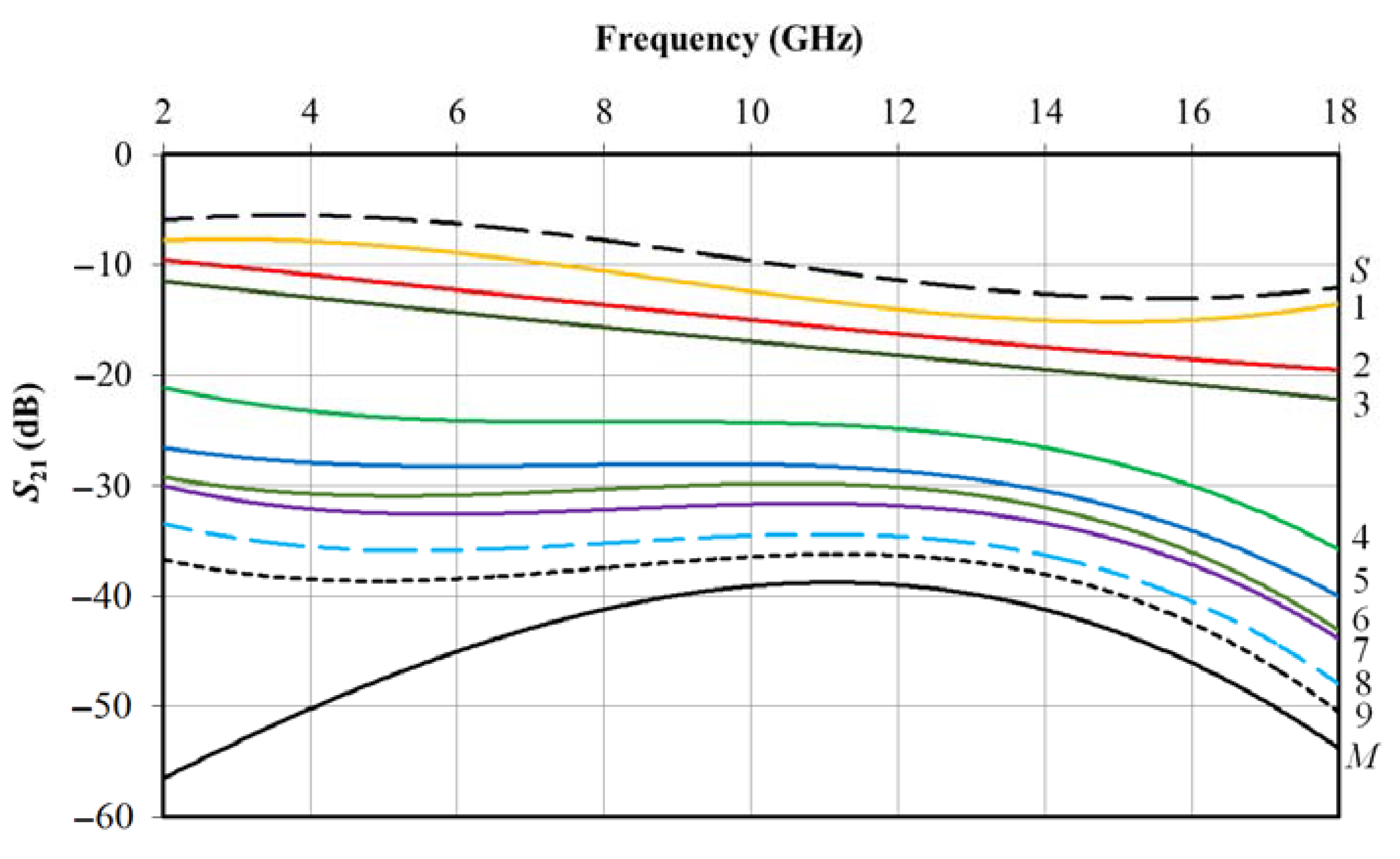
The frequency dependencies of the averaged values of the modulus of the transmission coefficient S21 for nickel thin film samples of various thickness are shown in Figure 6.
The graph indicated by S corresponds to the value of the modulus of the S21 coefficient (S21sub) obtained when the uncoated substrate is installed in the gap between the horn antennas; the graph indicated by M corresponds to a metal sheet 6 mm thick with overall dimensions equal to the overall dimensions of samples (l >> δ in the used frequency range).
The measurement results show a gradual approach of the values of S21 coefficient with the increase of the film thickness, to the results obtained for the metal sheet. The form of the obtained frequency dependencies is typical for continuous metal films and correlates with the literature data [39]. The main reason for the decrease in S21 coefficient with increasing frequency is an increase in the l/δ ratio, which clearly manifests itself for diamagnetic materials, for example, gold [40]. For the investigated ferromagnetic nickel films, the frequency dependence has a more complex form (in comparison with nonmagnetic metals). This is due to the nature of the change in the skin depth shown in Figure 3. Only for a film with a thickness of 4 nm, an increase in S21 coefficient is observed in the region of the upper part of the investigated frequency range, which may be due to a net-like structure of the film or even the presence of discontinuous islands [41,42]. However, the experimental results do not allow to directly confirm or refute this assumption based on the electrical resistivity value (see Figure 5b).
According to [22], for the estimation of SE in engineering calculations, the approximation of a plane electromagnetic wave and an infinite plane electromagnetic shield is used. Thus, the value of SE can be estimated depending on the l/δ ratio from the following equations:
S E = 30 π 2 ρ v e l δ ,   when   l / δ > 1 ;
S E = 60 π l ρ v ,   when   l / δ < 0.1 .
Obviously, when l ˃ δ, the value of SE increases significantly, and in the overwhelming majority of cases it becomes sufficient to effectively perform as an electromagnetic shield. In the second case, at l/δ ˂ 0.1, the expediency of using such electromagnetic shield depends on the possibility of providing the required SE value in a given frequency range or at a certain given frequency determined by the requirements of electromagnetic compatibility.
Equations (4) and (5) are approximation, implying the use of infinite flat shield without limiting the values of f, ρv and l.
An alternative calculation technique, based on the most commonly used approach according to [43], for layers with a thickness of l < 0.1δ is described in [1]. In accordance with it, the shielding effectiveness can be estimated from the following equation:
S E 1 R = 4 Z m Z 0
where R is the reflection coefficient; Z 0 is the impedance of the free space, Z 0 = 120 π 377   Ω , and Z m is the impedance of the metal surface, Z m = 2 π f μ μ 0 ρ v .
The calculated value of the modulus of the coefficient S21 in decibels can be found from the following equation [43]:
S 21 = 20 log 10 ( S E ) .
In the experimental studies, a thin metal coating is usually deposited on a substrate of a finite thickness, which increases the EMR power loss during measurements. For a correct comparison of the calculated and measured values of the coefficient S21, it is necessary to take into account the influence of the uncoated substrate on the measurement results. In this case, from the values of S21 found experimentally, it is necessary to subtract the values of S21 of the substrate (graph S in Figure 6).
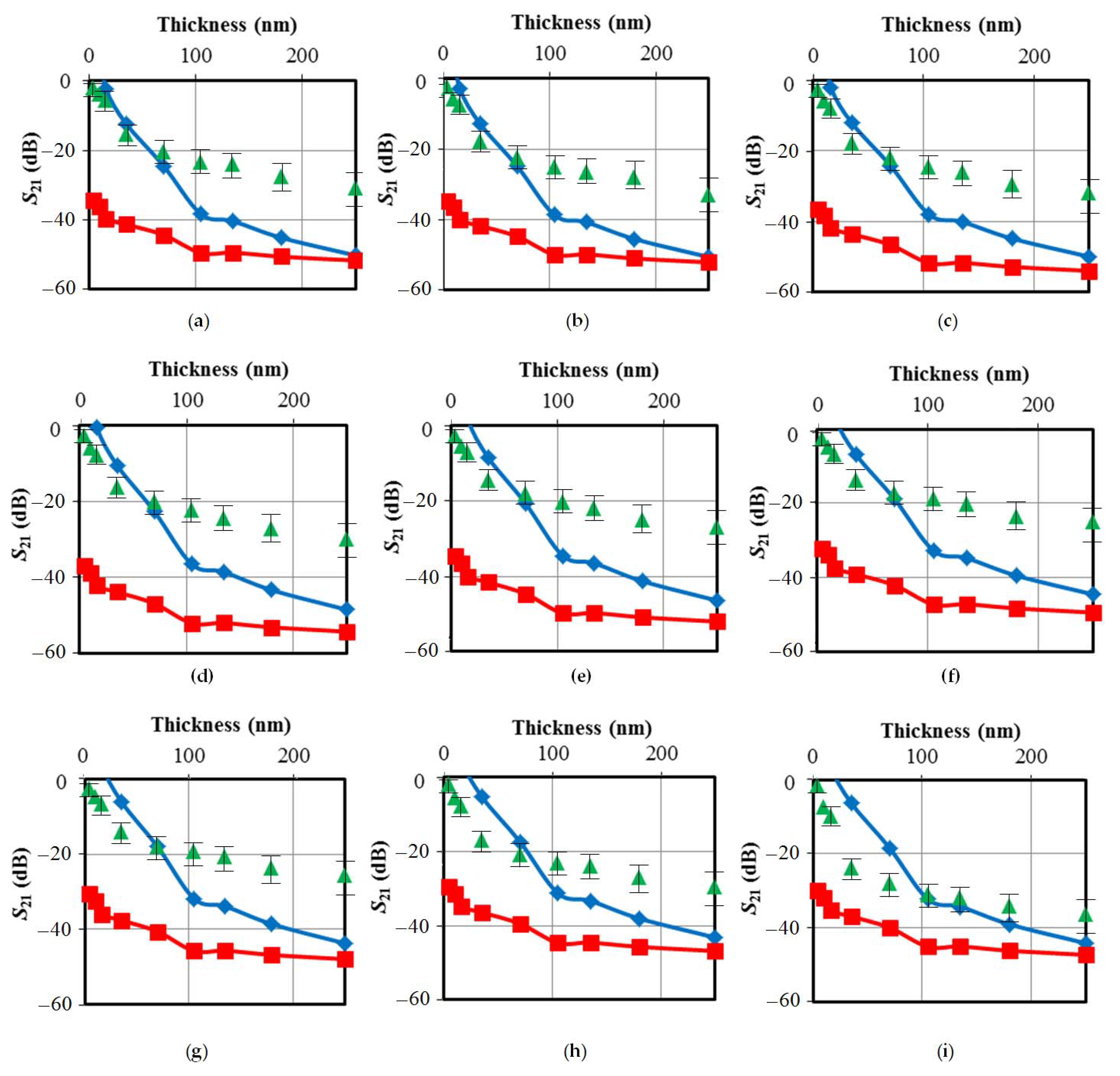
The dependencies of S21 versus the thickness of the nickel layer, obtained analytically using Equations (5)–(7) and in experimental studies, are shown in Figure 7.
The results in the frequency range from 2 to 12 GHz, obtained using Equation (5), better describe the experimental data compared to the results obtained using Equation (6). For films with a thickness of more than 100 nm, this trend persists up to frequencies of the order of 16 GHz.
The nature of the change in S21 with a change in the EMR frequency better reflects the results obtained by Equation (6), which gradually approach the calculated values as the film thickness increases. The thickness range can be separated in three regions: from 4 to 35 nm, from 35 to 100 nm, and from 100 to 250 nm. In these regions, the value of S21 has an almost linear dependence on l (for both the experimentally obtained results and the results obtained following Equation (6)). For these intervals, it is possible to calculate the correction factors depending on the type of receiving and transmitting antennas used in the portable closed measuring stand and the overall dimensions of the samples of the materials under study for calculating SE values in all ranges of the studied frequencies and thicknesses.
Nevertheless, if the precisely calculated SE values are required, various finite element software packages can be used, since the portable closed measuring stand with the horn antennas cannot be accurately described with the analytical models of acceptable complexity in engineering calculations. In addition, the approach used in this work does not take into account the formation of a nickel oxide layer, which has semiconducting properties and therefore affects the effective resistance of the entire structure. Apparently, for this reason, an accurate calculation using the above-mentioned software packages will require a more accurate setting and therefore a more sophisticated experimental study of the internal structure of thin films. Since nickel oxidation kinetics is diffusion-limited even for films with a thickness of about 10 nm at high temperatures [44], we suppose that the effect of the oxide layer formation can be neglected in the present engineering calculations.

4. Conclusions

It has been experimentally shown that DC magnetron sputtering technique allows to produce continuous nickel films with a thickness of 4–250 nm on glass and silicon substrates. The calculation of SE values for nickel thin films was performed taking into account the correction carried out on the basis of experimental data. The results of studies using a portable closed measuring stand of the frequency dependence of S21, obtained during measurements of a series of nickel thin films, correlate with the corresponding calculated S21 values. An increase in the measurement frequency and an increase in the thickness of the nickel film lead to a more accurate agreement between the experimental and calculated data.
The approach described in this work makes it possible to determine the dependence of the SE level on the thickness of the metal (magnetic and nonmagnetic) film. Nickel thin films up to 250 nm thick in the frequency range of 2–18 GHz provide SE of up to 35 dB. In the vast majority of cases, such SE values are sufficient for solving problems of electromagnetic shielding and electromagnetic compatibility.

Author Contributions

Conceptualization, O.A.T.; methodology, O.A.T. and A.E.K.; validation, V.V.L.; investigation, O.A.T., A.E.K., K.G.G., E.N.S. and I.O.T.; resources, O.A.T. and A.E.K.; data curation, K.G.G.; writing—original draft preparation, O.A.T.; writing—review and editing, A.E.K. and K.G.G.; supervision, V.V.L.; project administration, I.K.K.; funding acquisition, V.V.L. All authors have read and agreed to the published version of the manuscript.

Funding

This research was funded by Russian Science Foundation, Grant Number 21-19-00719.

Institutional Review Board Statement

Not applicable.

Informed Consent Statement

Not applicable.

Data Availability Statement

The data that support the finding of this research are not publicly available due to confidentiality constraints.

Conflicts of Interest

The authors declare no conflict of interest.

References

  1. Ott, H.W. Electromagnetic Compatibility Engineering; John Wiley & Sons: Hoboken, NJ, USA, 2009; pp. 243–252. [Google Scholar]
  2. Jiang, Z.; Zhao, S.; Huang, W.; Chen, L.; Liu, Y. Embedded flexible and transparent double-layer nickel-mesh for high shielding efficiency. Opt. Express 2020, 28, 26531–26542. [Google Scholar] [CrossRef] [PubMed]
  3. Angappan, M.; Bora, P.J.; Vinoy, K.J.; Ramamurthy, P.C.; Vijayaraju, K. Tailorable electromagnetic interference shielding using nickel coated glass fabric-epoxy composite with excellent mechanical property. Compos. Commun. 2018, 10, 110–115. [Google Scholar] [CrossRef]
  4. Chung, D.D.L. Electromagnetic interference shielding effectiveness of carbon materials. Carbon 2001, 39, 279–285. [Google Scholar] [CrossRef]
  5. Jiyong, H.; Guohao, L.; Junhui, S.; Xudong, Y.; Xin, D. Improving the electromagnetic shielding of nickel/polyaniline coated polytrimethylene-terephthalate knitted fabric by optimizing the electroless plating conditions. Text. Res. J. 2017, 87, 902–912. [Google Scholar] [CrossRef]
  6. Yu, X.; Shen, Z. The electromagnetic shielding of Ni films deposited on cenosphere particles by magnetron sputtering method. J. Magn. Magn. Mater. 2009, 321, 2890–2895. [Google Scholar] [CrossRef]
  7. Dravid, S.V.; Bhosale, S.D.; Datar, S.; Goyal, R.K. Nickel Nanoparticle-Filled High-Performance Polymeric Nanocomposites for EMI Shielding Applications. J. Electron. Mater. 2020, 49, 1630–1637. [Google Scholar] [CrossRef]
  8. Geetha, S.; Kumar, K.K.S.; Rao, C.R.K.; Vijayan, M.; Trivedi, D.C. EMI shielding: Methods and materials—A review. J. Appl. Polym. Sci. 2009, 112, 2073–2086. [Google Scholar] [CrossRef]
  9. Jiang, S.X.; Guo, R.H. Electromagnetic shielding and corrosion resistance of electroless Ni-P/Cu-Ni multilayer plated polyester fabric. Surf. Coat. Technol. 2011, 205, 4274–4279. [Google Scholar] [CrossRef]
  10. Ding, X.; Wang, W.; Wang, Y.; Xu, R.; Yu, D. High-performance flexible electromagnetic shielding polyimide fabric prepared by nickel-tungsten-phosphorus electroless plating. J. Alloys Compd. 2019, 777, 1265–1273. [Google Scholar] [CrossRef]
  11. Tran, V.V.; Nguyen, D.D.; Nguyen, A.T.; Hofmann, M.; Hsieh, Y.P.; Kan, H.C.; Hsu, C.C. Electromagnetic Interference Shielding by Transparent Graphene/Nickel Mesh Films. ACS Appl. Nano Mater. 2020, 3, 7474–7481. [Google Scholar] [CrossRef]
  12. Jordan, L.; Swanger, W.H. The properties of pure nickel. Bur. Stand. J. Res. 1930, 5, 1291–1307. [Google Scholar] [CrossRef]
  13. Lide, D.R. Handbook of Chemistry and Physics, 84th ed.; CRC Press: Boca Raton, FL, USA, 2004; pp. 1988–1990. [Google Scholar]
  14. Bogoroditsky, N.P.; Pasynkov, V.V.; Tareev, B.M. Electrical Engineering Materials; Mir Publishers: Moscow, Russia, 1979; p. 232. [Google Scholar]
  15. Dizenko, E.I.; Novoselov, V.F.; Tugunov, P.I.; Yufin, V.A. Corrosion Protection of Pipelines and Tanks; Nedra: Moscow, Russia, 1978; p. 24. (In Russian) [Google Scholar]
  16. Roberge, P.R. Handbook of Corrosion Engineering; McGraw-Hill: New York, NY, USA, 2000; p. 233. [Google Scholar]
  17. Revie, R.W.; Uhlig, H.H. Corrosion and Corrosion Control: An Introduction to Corrosion Science and Engineering, 4th ed.; John Wiley & Sons: Hoboken, NJ, USA, 2008; p. 220. [Google Scholar]
  18. Zhuk, N.P. A Course on the Theory of Corrosion and Protection of Metals; Metallurgiya: Moscow, Russia, 1976; pp. 32, 75, 76. (In Russian) [Google Scholar]
  19. Krynetskiĭ, I.B.; Gizhevskiĭ, B.A.; Naumov, S.V.; Kozlov, E.A. Size effect of the thermal expansion of nanostructural copper oxide. Phys. Solid State 2008, 50, 756–758. [Google Scholar] [CrossRef]
  20. Kazantsev, E.I. Industrial Ovens. Reference Guide for Calculations and Design, 2nd ed.; Supplemented and Revised; Metallurgiya: Moscow, Russia, 1975; p. 46. (In Russian) [Google Scholar]
  21. Gadzhiev, G.G. The thermal and elastic properties of zinc oxide-based ceramics at high temperatures. High Temp. 2003, 41, 778–782. [Google Scholar] [CrossRef]
  22. Shapiro, D.N. Fundamentals of the Theory of Electromagnetic Shielding; Energiya: Leningrad, Russia, 1975; p. 21. (In Russian) [Google Scholar]
  23. Maskaeva, L.N.; Fedorova, E.A.; Markov, V.F. Thin Film and Coating Technology; Publishing House of the Ural University: Yekaterinburg, Russia, 2019; pp. 11–14. (In Russian) [Google Scholar]
  24. Jackson, B.C.; Shawhan, G. Current review of the performance characteristics of conductive coatings for EMI control. In Proceedings of the IEEE International Symposium on Electromagnetic Compatibility, Denver, CO, USA, 24–28 August 1998; Volume 1, pp. 567–572. [Google Scholar] [CrossRef]
  25. Smits, F.M. Measurement of Sheet Resistivities with the Four-Point Probe. Bell Syst. Tech. J. 1958, 37, 711–718. [Google Scholar] [CrossRef]
  26. Haldor Topsoe Semiconductor Division. Geometric Factors in Four Point Resistivity Measurement; Bulletin No. 472-13; Haldor Topsøe: Vedbæk, Denmark, 1966; Volume 472, p. 15. [Google Scholar]
  27. Marvin, A.C.; Dawson, L.; Flintoft, I.D.; Dawson, J.F. A method for the measurement of shielding effectiveness of planar samples requiring no sample edge preparation or contact. IEEE Trans. Electromagn. Compat. 2009, 51, 255–262. [Google Scholar] [CrossRef] [Green Version]
  28. Volski, V.; Vandenbosch, G.A.E.; Vasylchenko, A. A dedicated technique to measure shielding effectiveness of textiles using a two-horn antenna set-up. J. Text. Inst. 2011, 102, 164–171. [Google Scholar] [CrossRef]
  29. Wang, L.-B.; Zhang, J.-W.; See, K.Y.; Svimonishvili, T. Ultra-Thin and Flexible Multi-Band Rejection EMI Shield. J. Electromagn. Anal. Appl. 2014, 6, 163–173. [Google Scholar] [CrossRef] [Green Version]
  30. Cui, Y. A New Measure for Evaluating Shielding Performance of an Equipment Enclosure at Frequencies above 1 GHz. Ph.D. Thesis, Department of Electronics, University of York, York, UK, 2007. [Google Scholar]
  31. Andryushchenko, M.S.; Gusakovskii, V.E.; Shtager, E.A.; Shtager, D.E.; Shchesnyak, S.S. Methods of Analysis of EMI Protection of Radioelectronic Systems; VVM: St. Petersburg, Russia, 2016; pp. 271–273. (In Russian) [Google Scholar]
  32. Gareev, K.G.; Luchinin, V.V.; Sevost’yanov, E.N.; Testov, I.O.; Testov, O.A. Frequency Dependence of an Electromagnetic Absorption Coefficient in Magnetic Fluid. Tech. Phys. 2019, 64, 893–896. [Google Scholar] [CrossRef]
  33. Tao, Y.; Scharf, F. Revisiting the Effect of Nickel Characteristics on High-Speed Interconnect Performance. IEEE Trans. Microw. Theory Tech. 2016, 64, 2447–2453. [Google Scholar] [CrossRef]
  34. Timsit, R.S. High speed electronic connector design: A review of electrical and electromagnetic properties of passive contact. IEICE Trans. Electron. 2008, E91-C, 1178–1191. [Google Scholar] [CrossRef]
  35. Glathart, J.L. The inner, initial, magnetic permeability of iron and nickel at ultra-high radiofrequencies. Phys. Rev. 1939, 55, 833–838. [Google Scholar] [CrossRef]
  36. Hoag, J.B.; Glathart, J.L. The outer, initial permeability of nickel from 10 to 70 megacycles. Phys. Rev. 1940, 57, 240. [Google Scholar] [CrossRef]
  37. Nonaka, Y.; Nakane, H.; Maeda, T.; Hasuike, K. Simultaneous Measurement of the Resistivity and Permeability of a Film Sample with a Double Coil. IEEE Trans. Instrum. Meas. 1995, 44, 679–682. [Google Scholar] [CrossRef]
  38. Lucyszyn, S. Microwave characterization of nickel. In Proceedings of the Progress in Electromagnetics Research Symposium, Hangzhou, China, 24–28 March 2008; pp. 879–883. [Google Scholar]
  39. Choi, H.S.; Suh, S.J.; Kim, S.W.; Kim, H.J.; Park, J.W. Transparent electromagnetic shielding film utilizing imprinting-based micro patterning technology. Polymers 2021, 13, 738. [Google Scholar] [CrossRef]
  40. Liao, S.Y. Light Transmittance and RF Shielding Effectiveness of a Gold Film on a Glass Substrate. IEEE Trans. Electromagn. Compat. 1975, EMC-17, 211–216. [Google Scholar] [CrossRef]
  41. Liu, H.D.; Zhao, Y.P.; Ramanath, G.; Murarka, S.P.; Wang, G.C. Thickness dependent electrical resistivity of ultrathin (<40 nm) Cu films. Thin Solid Film. 2001, 384, 151–156. [Google Scholar] [CrossRef]
  42. Antonets, I.V.; Kotov, L.N.; Shavrov, V.G.; Shcheglov, V.I. Conducting and reflecting properties of nanometer-width films of various metals. J. Commun. Technol. Electron. 2006, 51, 1394–1400. [Google Scholar] [CrossRef]
  43. Schulz, R.B.; Plantz, V.C.; Brush, D.R. Shielding Theory and Practice. IEEE Trans. Electromagn. Compat. 1988, 30, 187–201. [Google Scholar] [CrossRef]
  44. Unutulmazsoy, Y.; Merkle, R.; Fischer, D.; Mannhart, J.; Maier, J. The oxidation kinetics of thin nickel films between 250 and 500 °C. Phys. Chem. Chem. Phys. 2017, 19, 9045–9052. [Google Scholar] [CrossRef] [PubMed] [Green Version]
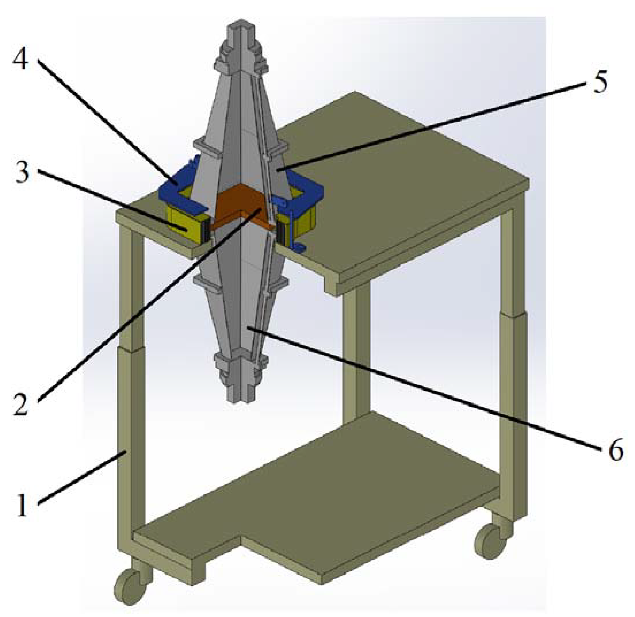
Figure 1. Measurement scheme using a portable closed measuring stand: 1—table; 2—test sample; 3—shield; 4—fasteners; 5—transmitting horn antenna; 6—receiving horn antenna.
Coatings 11 01455 g001
Figure 2. Frequency dependence of magnetic permeability of nickel in the range of 0–12 GHz, built by Equation (2).
Coatings 11 01455 g002
Figure 3. Frequency dependence of δ for chemically pure nickel (bulk material).
Coatings 11 01455 g003
Figure 4. Results of atomic force microscopy (AFM) study of the nickel thin film sample with a thickness of 70 nm: (a) thickness, z; (b) AFM surface image; (c) AFM microrelief scan.
Coatings 11 01455 g004
Figure 5. Dependence of the sheet resistance, ρs (a) and electrical resistivity, ρv (b) versus the nickel thin film thickness.
Coatings 11 01455 g005
Figure 6. Frequency dependencies of S21 coefficient: S—the cell with a substrate without metallization; 1–4 nm; 2–10 nm; 3–16 nm; 4–35 nm; 5–70 nm; 6–110 nm; 7–135 nm; 8–180 nm; 9–250 nm; M—metal sheet with overall dimensions corresponding to the dimensions of the samples.
Coatings 11 01455 g006
Figure 7. Experimental and calculated dependencies of S21 versus thickness of nickel thin films at different frequencies: (a) 2 GHz, (b) 4 GHz, (c) 6 GHz, (d) 8 GHz, (e) 10 GHz, (f) 12 GHz, (g) 14 GHz, (h) 16 GHz, (i) 18 GHz; —values obtained experimentally; —values calculated using Equations (5) and (7); —values calculated using Equations (6) and (7).
Coatings 11 01455 g007
Table 1. Thickness of samples of nickel thin films.
Sample No.Thickness (nm)
14
210
316
435
570
6110
7135
8180
9250
Publisher’s Note: MDPI stays neutral with regard to jurisdictional claims in published maps and institutional affiliations.