Author Contributions
Conceptualization, C.A., A.S.A., A.B. (Alessandro Bertarelli), N.B., F.C. (Federico Carra), F.C. (Fritz Caspers), J.G.V., A.K., E.M., S.R., B.S., M.T. and W.V.; Data curation, C.A., A.S.A., N.B., J.G.V. and A.K.; Formal analysis, C.A., A.S.A., N.B., S.C., J.G.V. and A.K.; Funding acquisition, A.B. (Alessandro Bertarelli) and S.R.; Investigation, C.A., D.A., A.S.A., A.B. (Adrienn Baris), N.B., F.C. (Fritz Caspers), E.G.-T.V., J.G.V., A.K., A.M., E.M., S.R., B.S., M.T. and W.V.; Methodology, C.A., A.S.A., N.B., S.C., F.C. (Fritz Caspers), J.G.V. and A.K.; Project administration, A.B. (Alessandro Bertarelli), E.M., S.R. and B.S.; Resources, C.A., N.B., F.C. (Fritz Caspers), J.G.V., A.K., B.S. and W.V.; Software, C.A., A.S.A., N.B., S.C., J.G.V. and A.K.; Supervision, C.A., A.S.A., N.B., F.C. (Carra Federico), J.G.V., E.M., S.R., B.S., M.T. and W.V.; Validation, C.A., D.A., A.S.A., A.B. (Adrienn Baris), A.B. (Alessandro Bertarelli), N.B., S.C., F.C. (Carra Federico), F.C. (Fritz Caspers), E.G.-T.V., J.G.V., A.K., A.M., E.M., S.R., B.S., M.T. and W.V.; Visualization, C.A., A.S.A., A.B. (Adrienn Baris), N.B., E.G.-T.V., J.G.V., A.K., A.M. and S.R.; Writing—original draft, C.A., A.S.A., N.B., J.G.V., A.K., A.M., S.R., M.T. and W.V.; Writing—review and editing, C.A., D.A., A.S.A., A.B. (Adrienn Baris), A.B. (Alessandro Bertarelli), N.B., S.C., F.C. (Carra Federico), F.C. (Fritz Caspers), E.G.-T.V., J.G.V., A.K., A.M., E.M., S.R., B.S., M.T. and W.V. All authors have read and agreed to the published version of the manuscript.
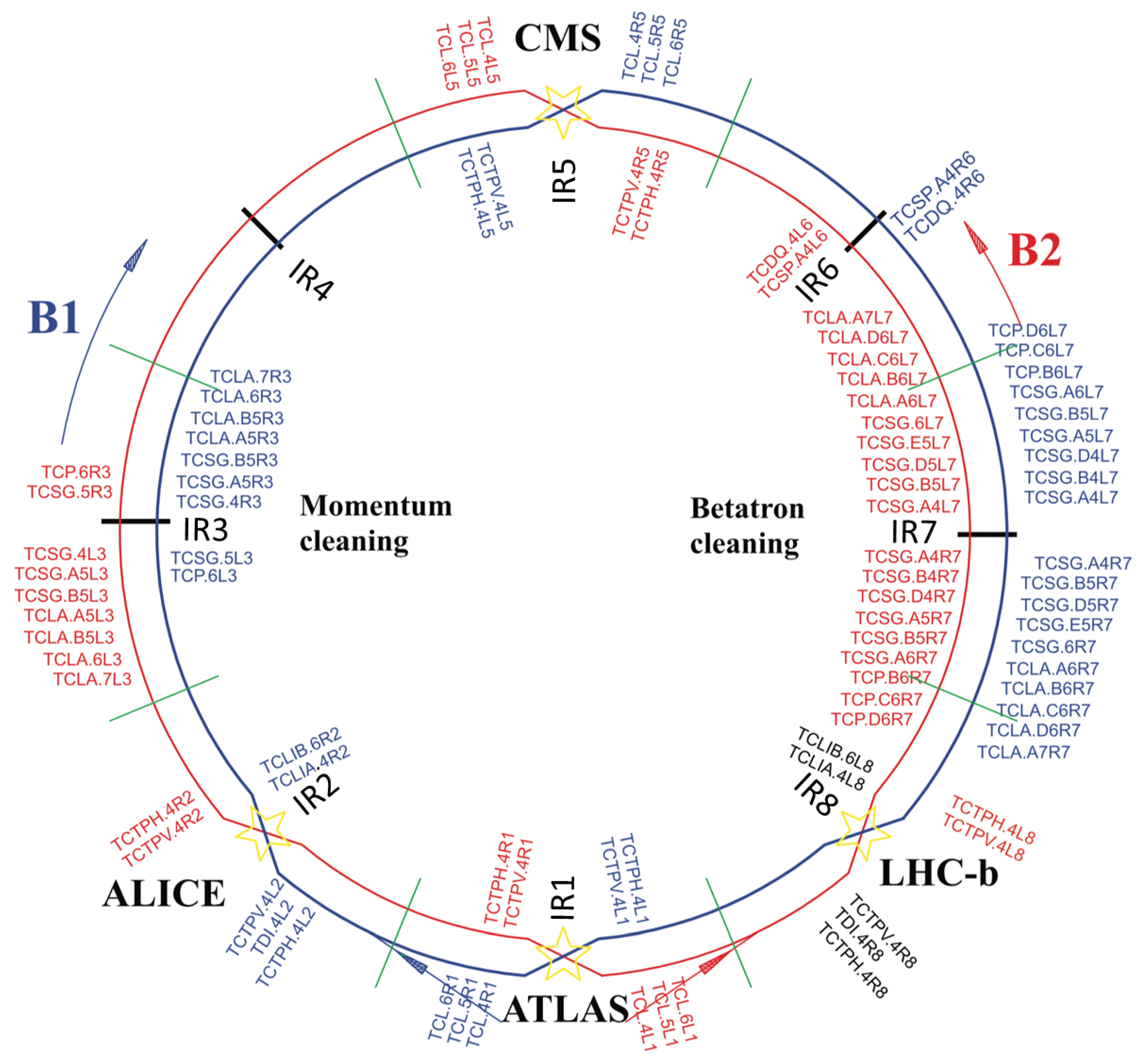
Figure 1.
Schematic representation of the LHC collimation system during Run 2 (2015–2018) [
8].
Figure 1.
Schematic representation of the LHC collimation system during Run 2 (2015–2018) [
8].
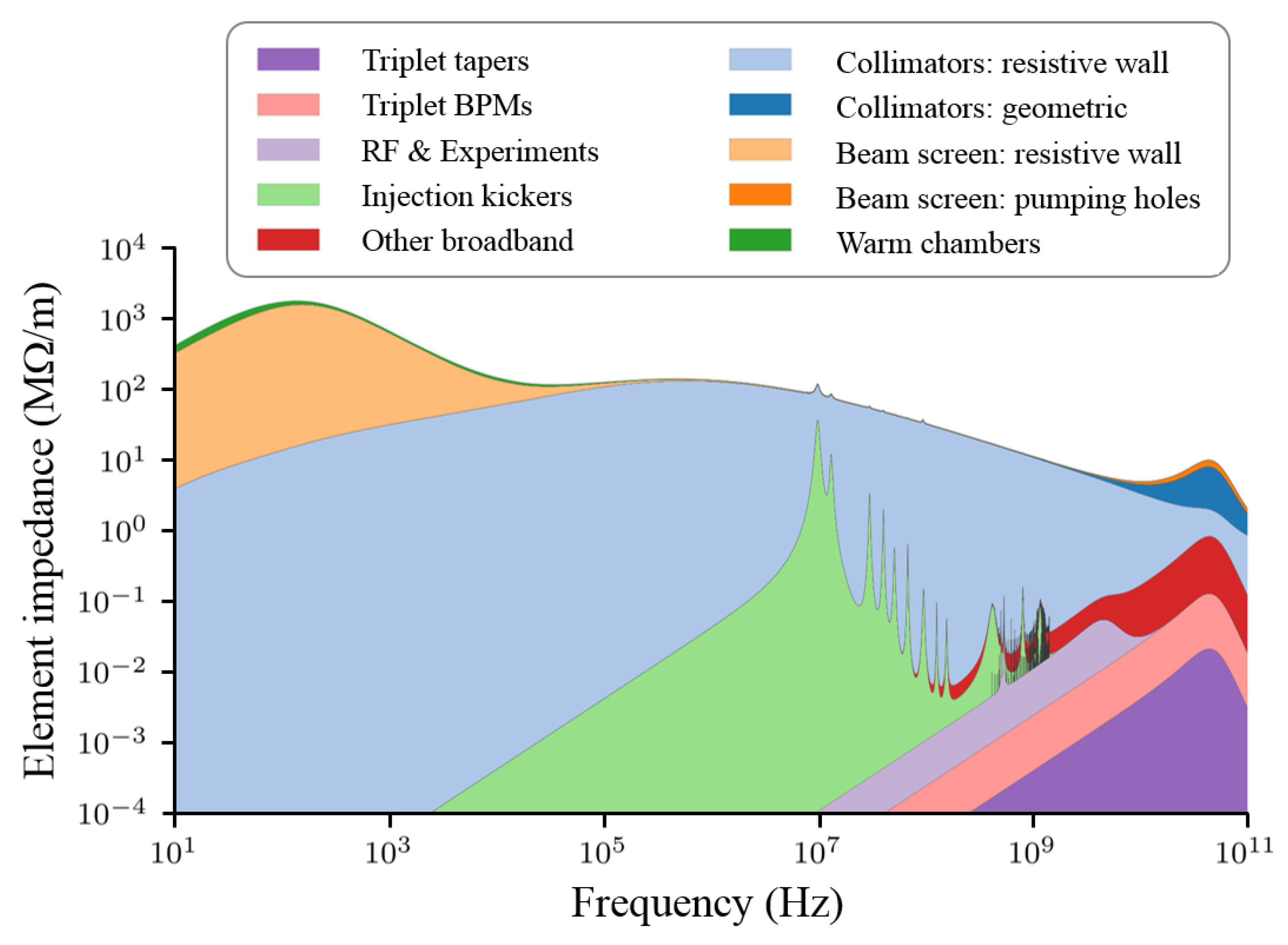
Figure 2.
Real part of the horizontal impedance of the LHC at 6.5 TeV for the different elements currently included in the LHC impedance model. The collimator horizontal impedance (shown in light blue) is clearly dominating over a wide range of frequencies. individual components are added on top of one another in the order of the legend.
Figure 3.
Octupole current needed to stabilize the BCMS beam under different collimator cases: present CFC primary and secondary collimators (violet bar), all the secondary collimators in IR7 upgraded to MoGr (yellow bar), and HL-LHC baseline with 9 out of 11 Mo-coated secondary collimators in IR7 (red bar). In all the upgrade scenarios two IR7 primary collimators are upgraded to MoGr jaws. The dashed line shows the maximum achievable octupole current of 570 A. The estimates assume a single-beam stability threshold with a factor 2 safety margin to account for additional destabilizing effects ranging from the imperfections of the impedance model and the optics to hardware noise. More details on the estimates can be found in [
24,
26].
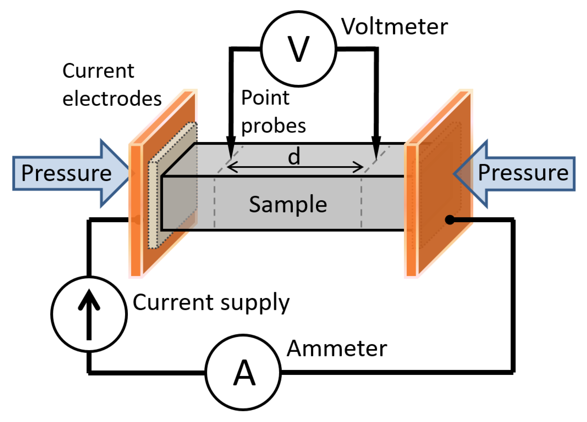
Figure 4.
Scheme of the four-probe setup used for bulk measurements.
Figure 4.
Scheme of the four-probe setup used for bulk measurements.
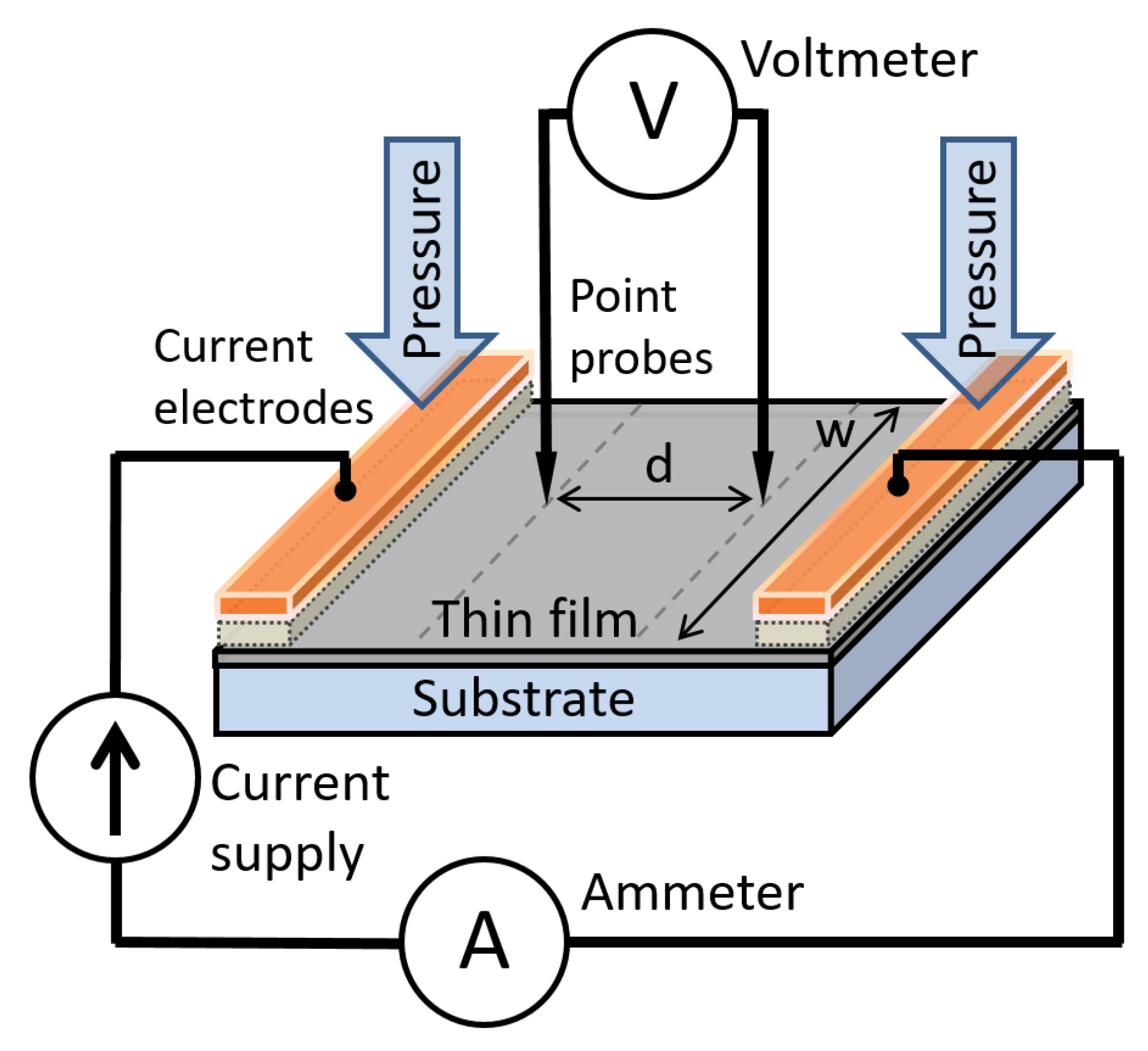
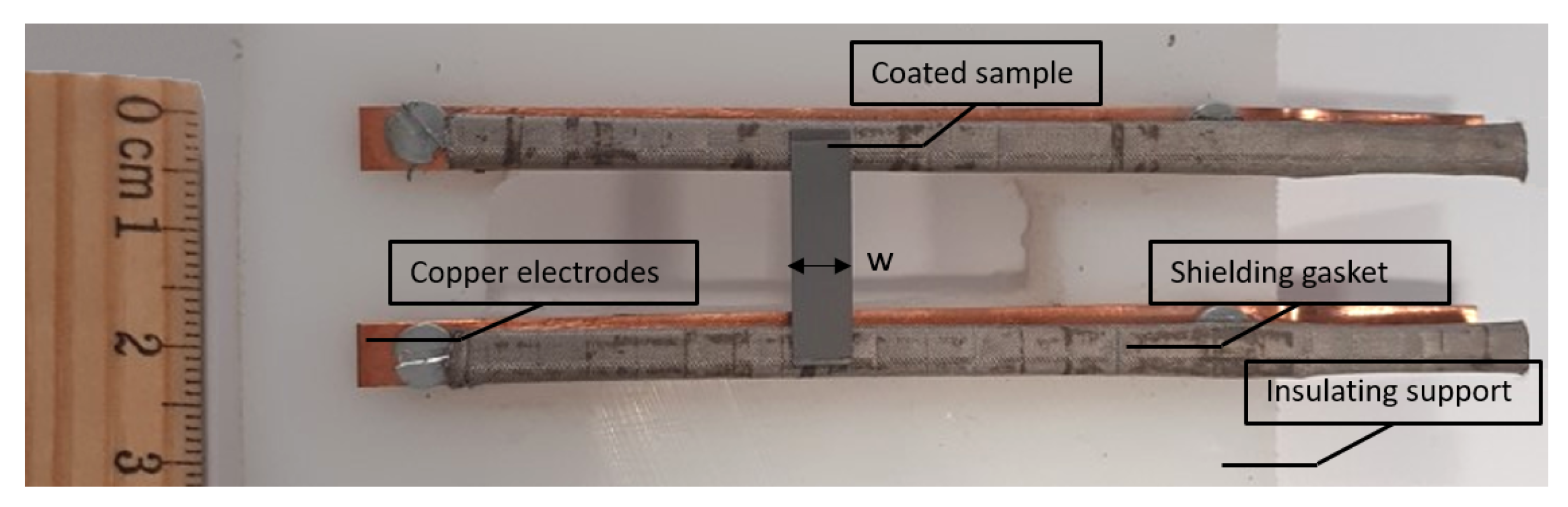
Figure 5.
Scheme of the four-probe setup used for thin film measurements.
Figure 5.
Scheme of the four-probe setup used for thin film measurements.
Figure 6.
Back-view of the setup for coating DC resistivity measurement.
Figure 6.
Back-view of the setup for coating DC resistivity measurement.
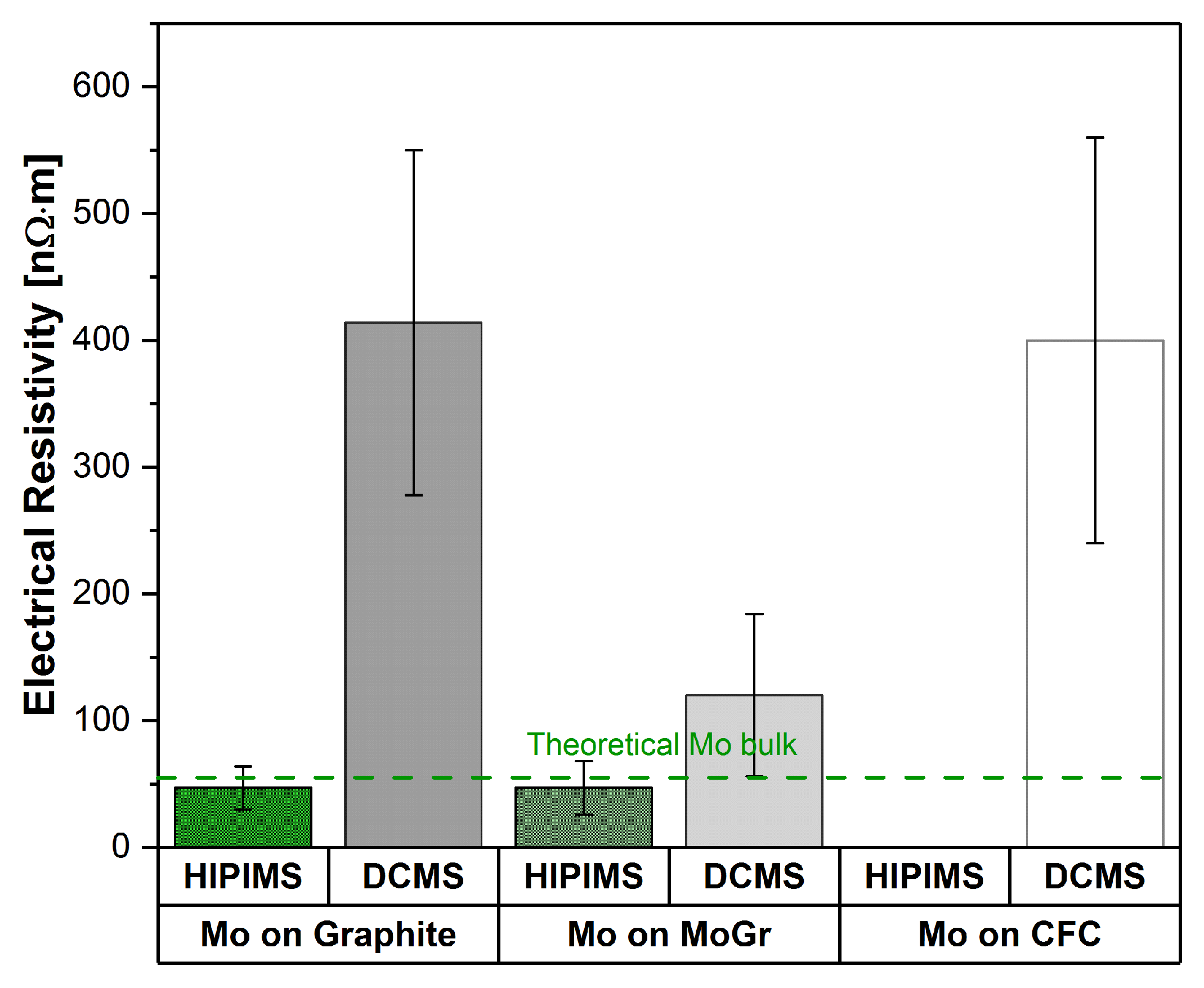
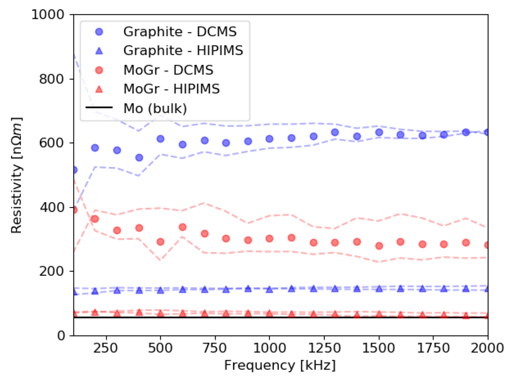
Figure 7.
Comparison of measured resistivity of Mo coating layers produced with HIPMS and DCMS techniques on graphite, MoGr and CFC substrates.
Figure 7.
Comparison of measured resistivity of Mo coating layers produced with HIPMS and DCMS techniques on graphite, MoGr and CFC substrates.
Figure 8.
ECT schematic representation.
Figure 8.
ECT schematic representation.
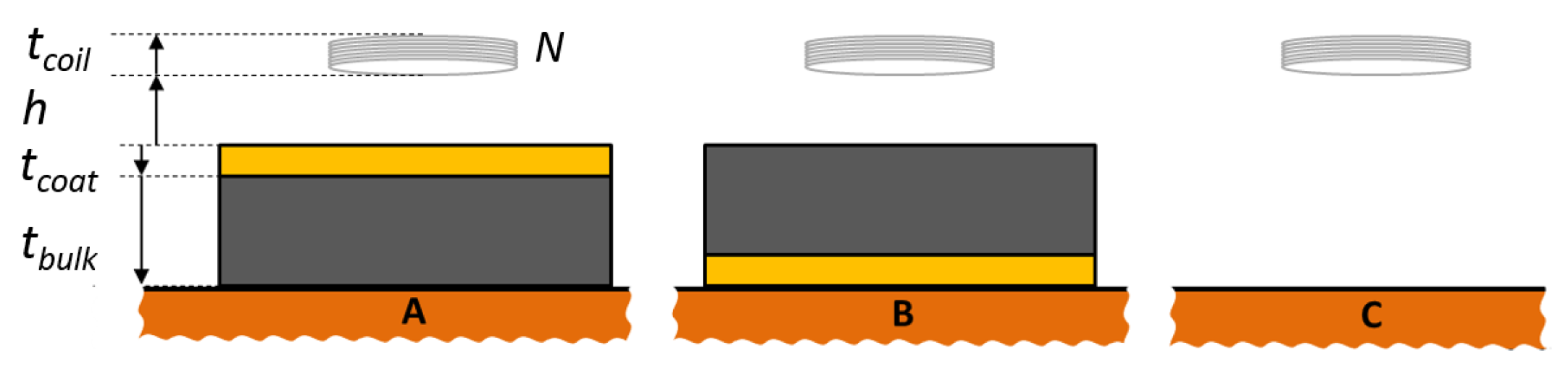
Figure 9.
ECT schematic procedure for resistivity measurements. Measurements in configurations B versus C give information on bulk resistivity and lift-off h; the measurement in configuration A versus B gives information on the coating resistivity. The thickness of the N-turns coil, of the coating and the bulk are also shown. The configuration C is taken with respect to the common substrate.
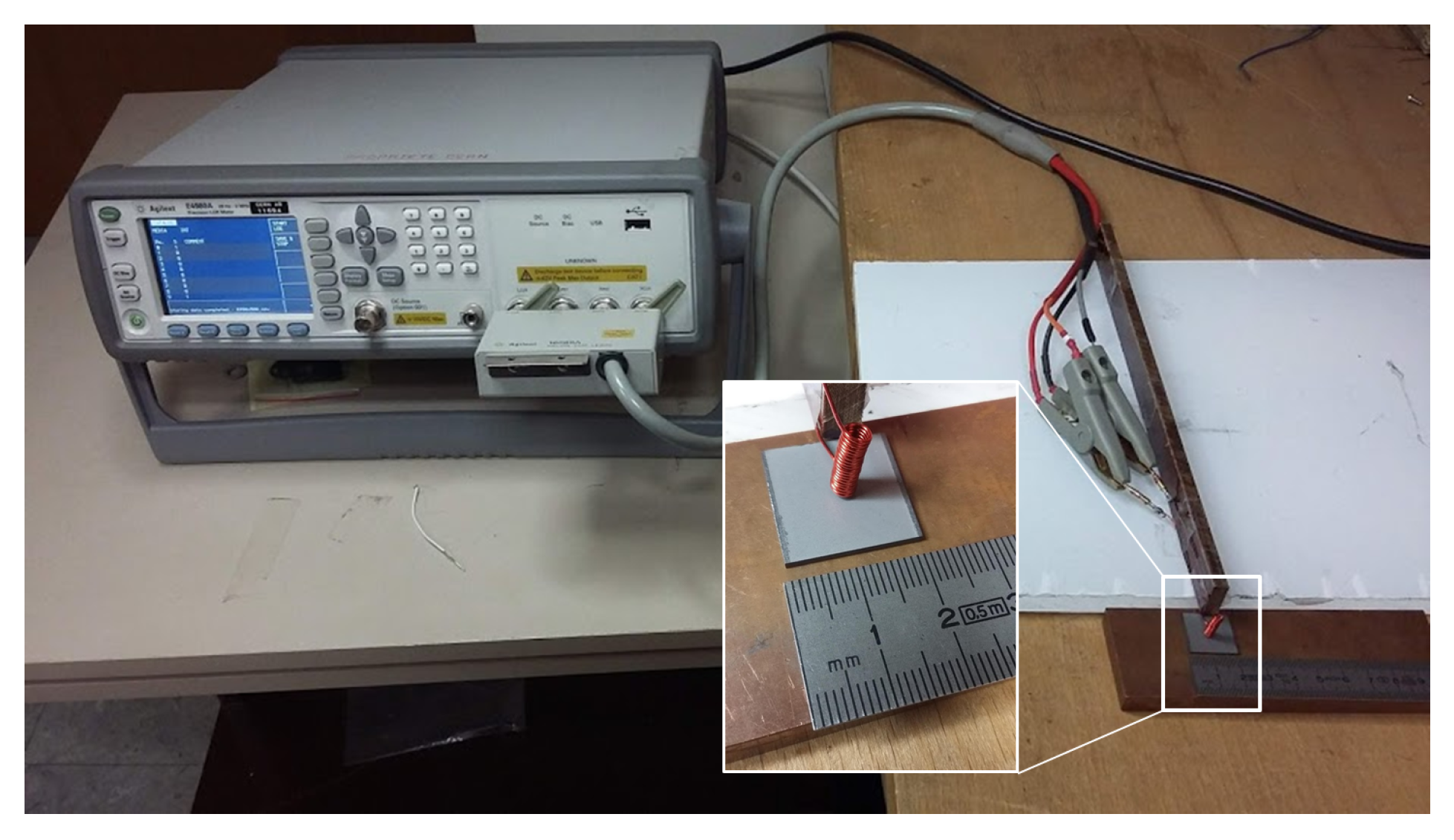
Figure 10.
ECT setup. The impedance analyzer is connected to a coil suspended over a sample under test.
Figure 10.
ECT setup. The impedance analyzer is connected to a coil suspended over a sample under test.
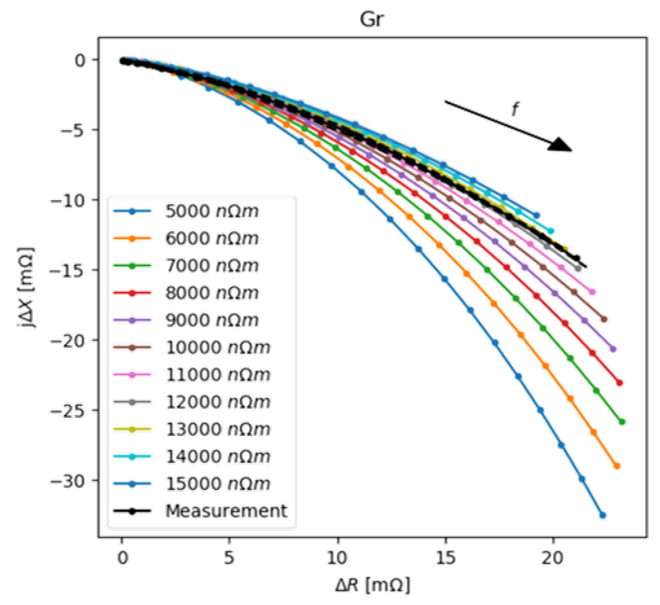
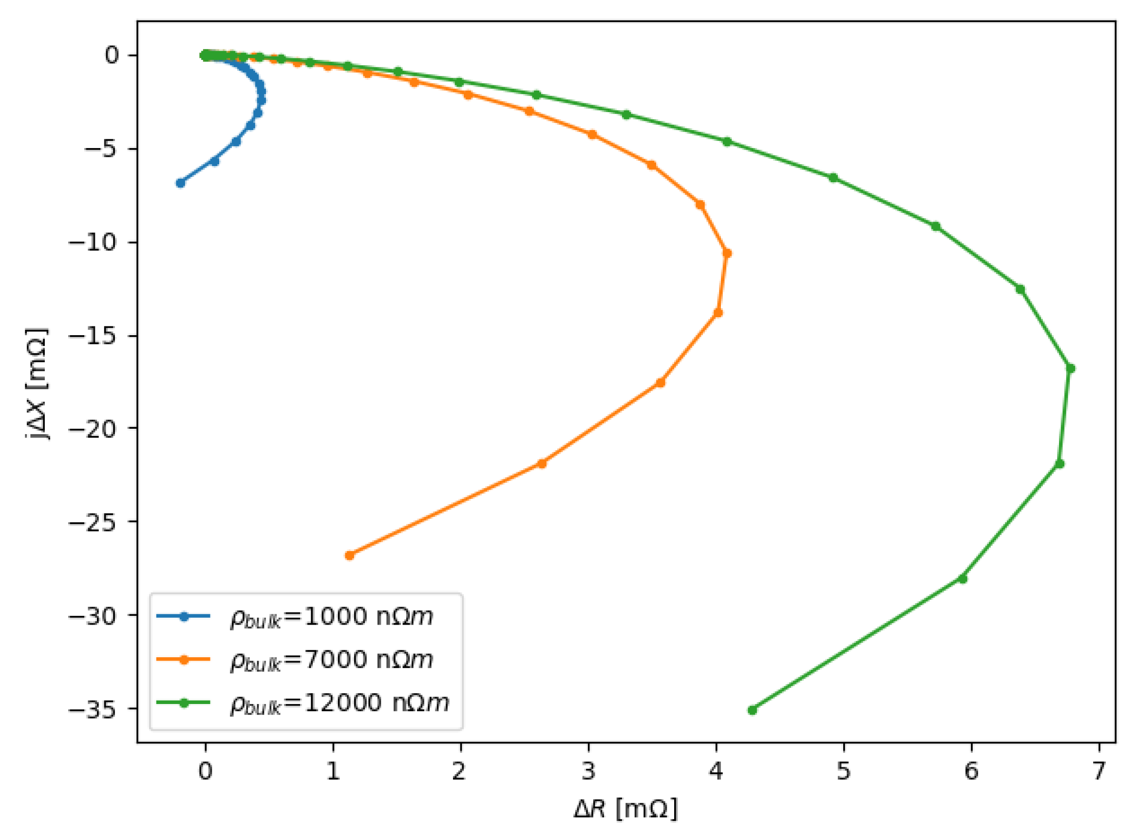
Figure 11.
Response of the coil on a graphite substrate of 1.5 mm thickness and mm lift-off (measured data with dashed lines representing the measurement standard deviation) compared to different simulated responses varying the bulk resistivity between 5000 nΩm and 15,000 nΩm.
Figure 11.
Response of the coil on a graphite substrate of 1.5 mm thickness and mm lift-off (measured data with dashed lines representing the measurement standard deviation) compared to different simulated responses varying the bulk resistivity between 5000 nΩm and 15,000 nΩm.
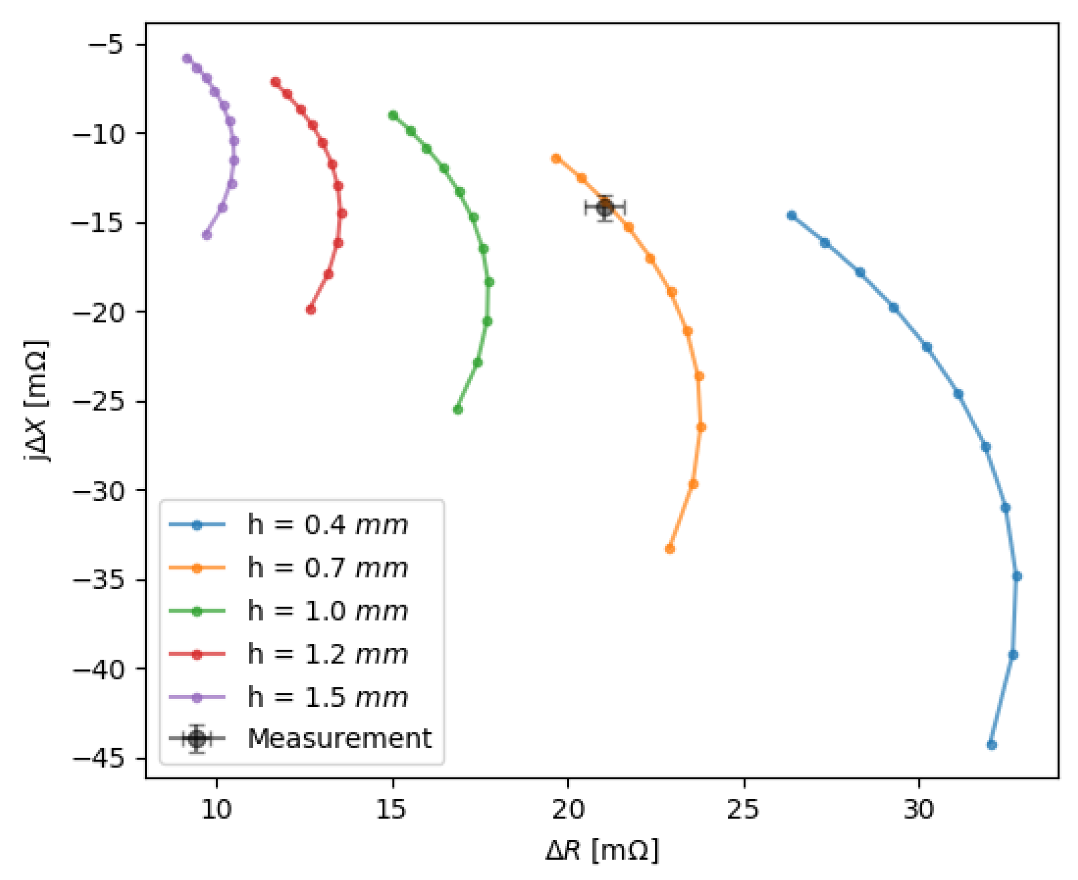
Figure 12.
Response of the coil on a graphite substrate for the maximum acquisition frequency of MHz with simulated responses for different lift-off parameters h and bulk resistivity between 5000 nΩm and 15,000 nΩm. The intersection of the curves with the data-point gives the actual lift-off of the measurement, i.e., mm.
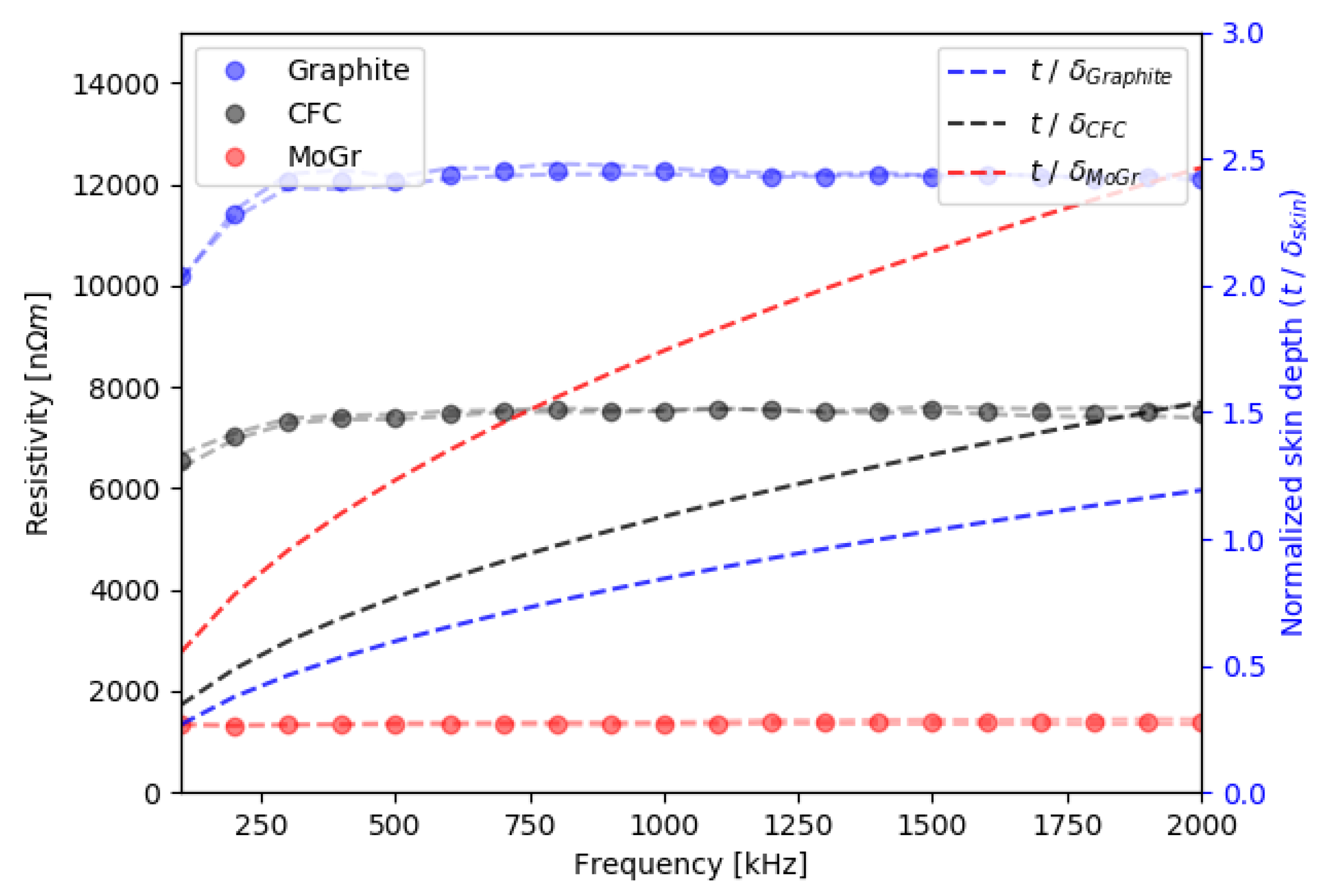
Figure 13.
Measured resistivity for CFC, graphite and MoGr samples as a function of frequency (dotted lines) together with sample thickness normalized to the material penetration depth (dashed lines).
Figure 13.
Measured resistivity for CFC, graphite and MoGr samples as a function of frequency (dotted lines) together with sample thickness normalized to the material penetration depth (dashed lines).
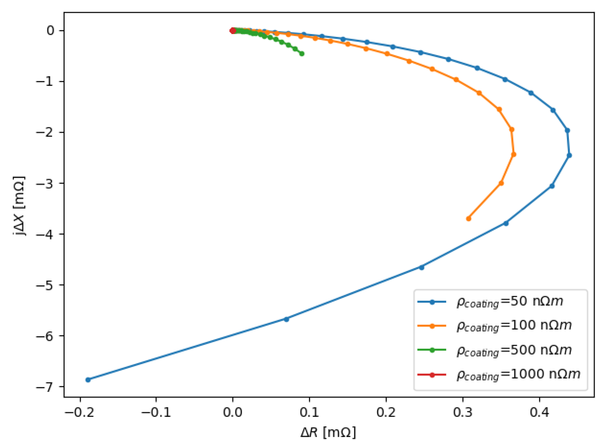
Figure 14.
Simulated coil response for variable coating resistivity as a function of frequency. We assume a bulk of 1.5 mm thickness, with a resistivity of 1000 nΩm, and a coating of 6 μm thickness. The lift-off is mm.
Figure 14.
Simulated coil response for variable coating resistivity as a function of frequency. We assume a bulk of 1.5 mm thickness, with a resistivity of 1000 nΩm, and a coating of 6 μm thickness. The lift-off is mm.
Figure 15.
Simulated coil response for variable bulk resistivity. We assume a bulk of 1.5 mm thickness, and a coating of 6 μm thickness with resistivity of 50 nΩm. The lift-off is mm.
Figure 15.
Simulated coil response for variable bulk resistivity. We assume a bulk of 1.5 mm thickness, and a coating of 6 μm thickness with resistivity of 50 nΩm. The lift-off is mm.
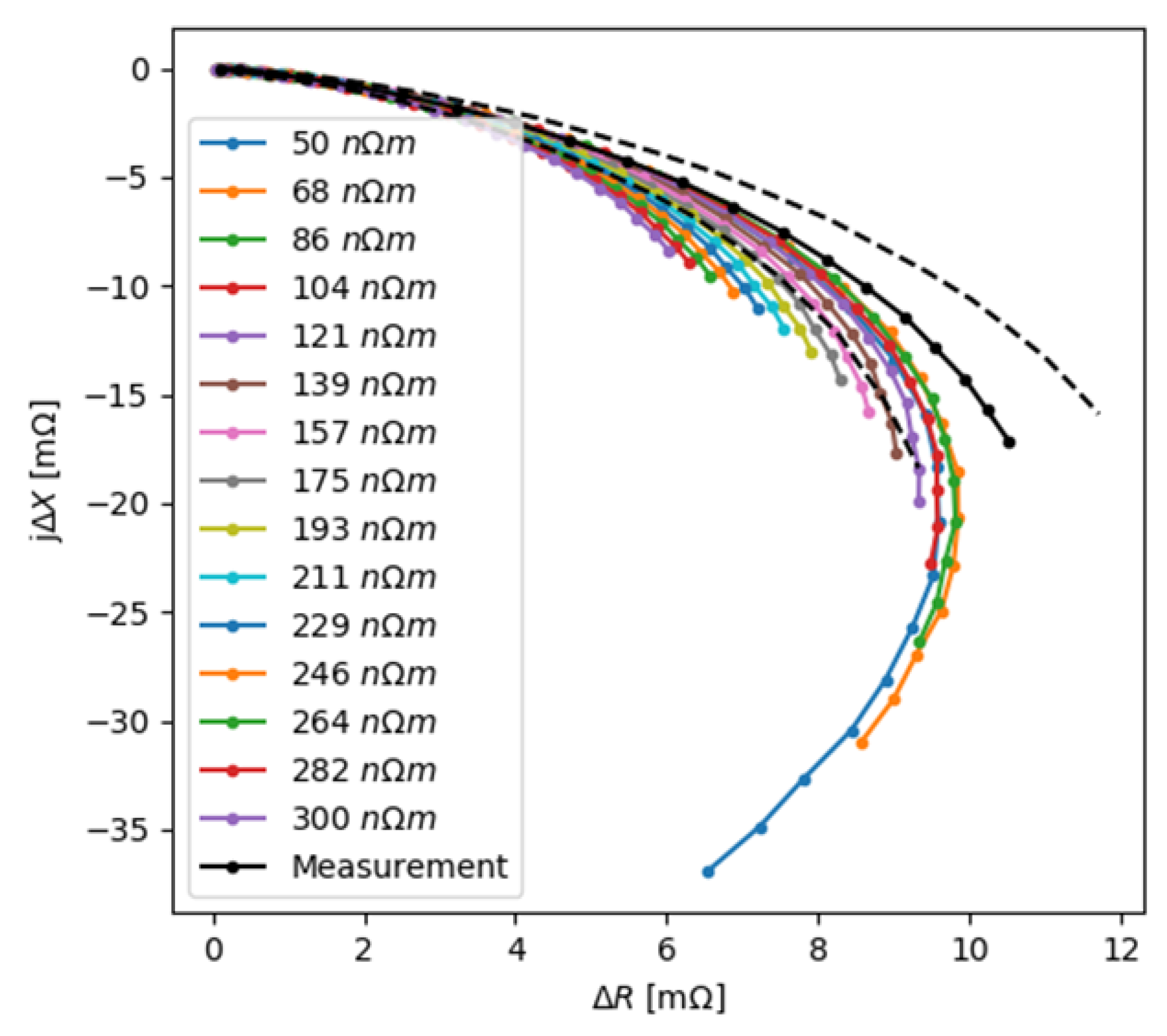
Figure 16.
Coil response for HIPIMS Mo coating on graphite. The measurements are shown with black lines together with standard deviation (dashed lines) and the simulated response for coating resistivity between 50 nΩm and 300 nΩm. The coating has a thickness of 6 μm, the bulk of 1.5 mm. The lift-off is 0.7 mm.
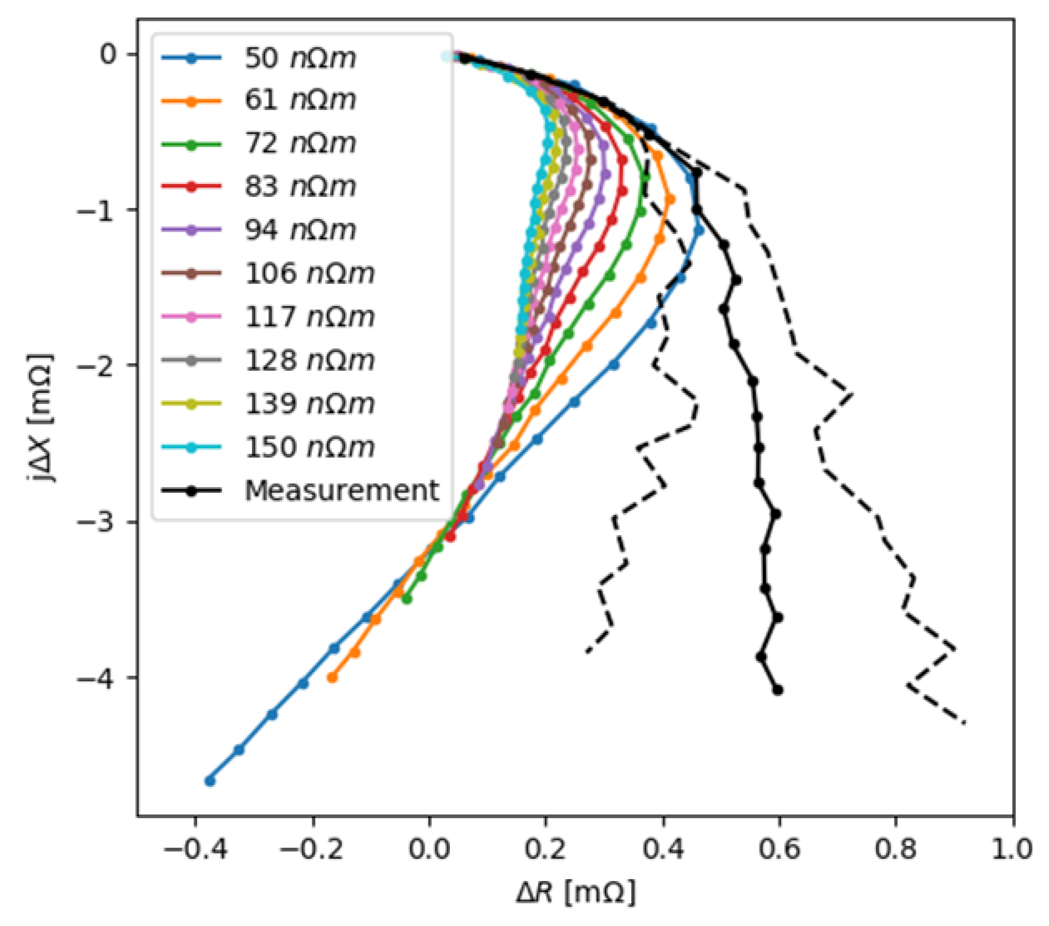
Figure 17.
Coil response for HIPIMS Mo coating on MoGr. The measurements are shown with black lines together with the standard deviation (dashed lines) and the simulated response for coating resistivity between 50 nΩm and 300 nΩm. The coating has a thickness of 6 μm, the bulk of 1 mm. The lift-off is 0.7 mm.
Figure 18.
ECT measurement of Mo resistivity on graphite and MoGr for DCMS and HIPIMS.
Figure 18.
ECT measurement of Mo resistivity on graphite and MoGr for DCMS and HIPIMS.
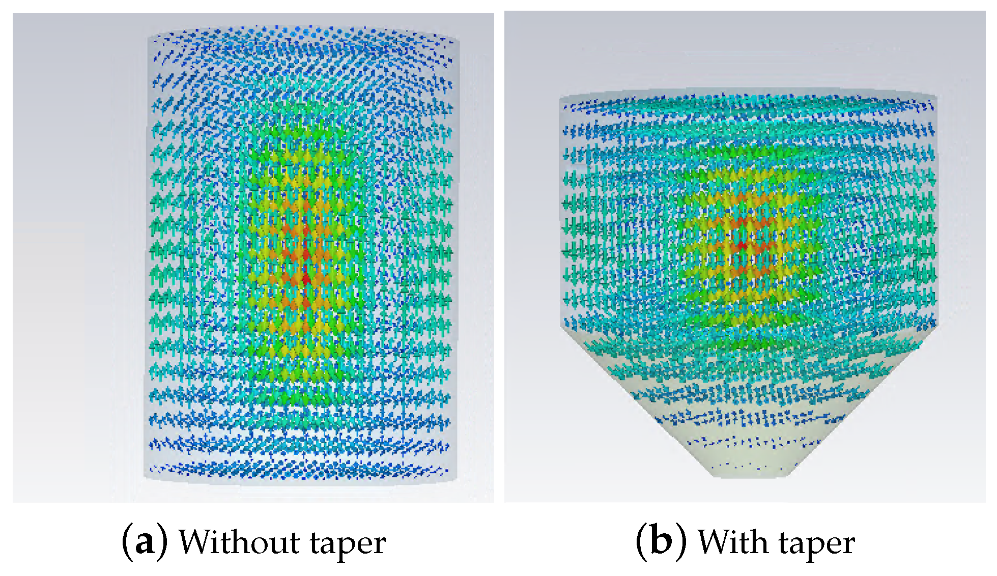
Figure 19.
H011 mode magnetic field distributions in a cylinder cavity without tapers (a), and with taper (b).
Figure 19.
H011 mode magnetic field distributions in a cylinder cavity without tapers (a), and with taper (b).
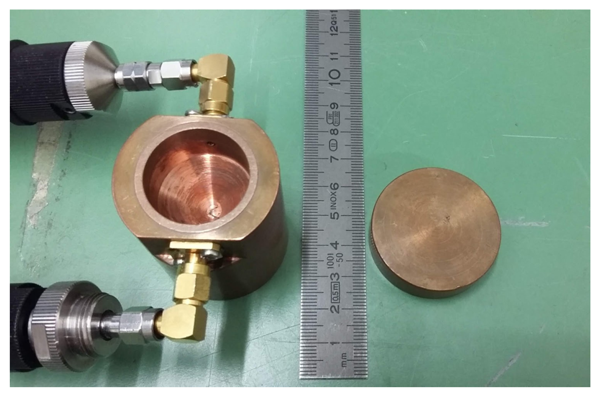
Figure 20.
Fabricated cylindrical resonator with removable end cap.
Figure 20.
Fabricated cylindrical resonator with removable end cap.
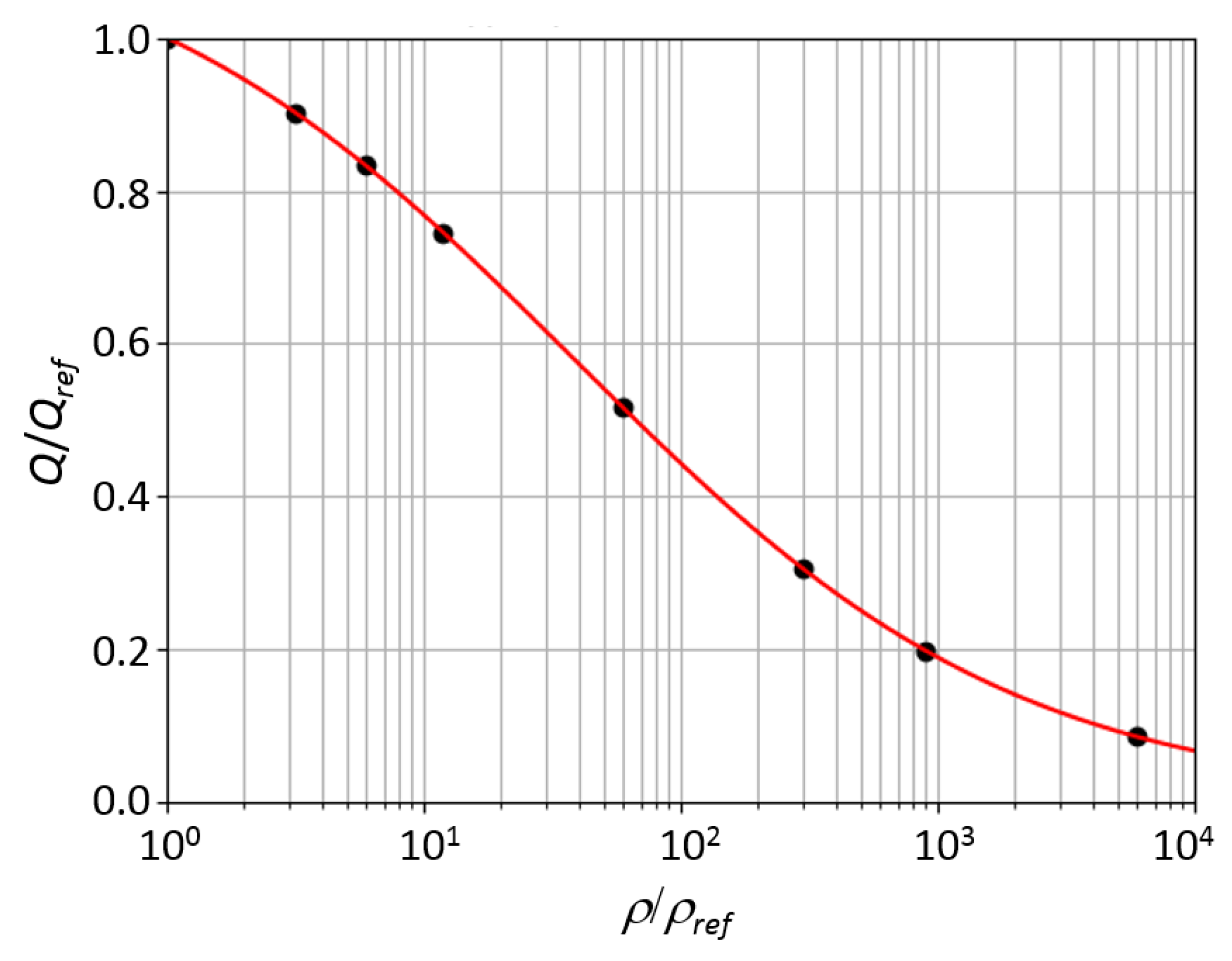
Figure 21.
CST Eigenmode simulation of the Q factor variation versus resistivity, normalized to copper.
Figure 21.
CST Eigenmode simulation of the Q factor variation versus resistivity, normalized to copper.
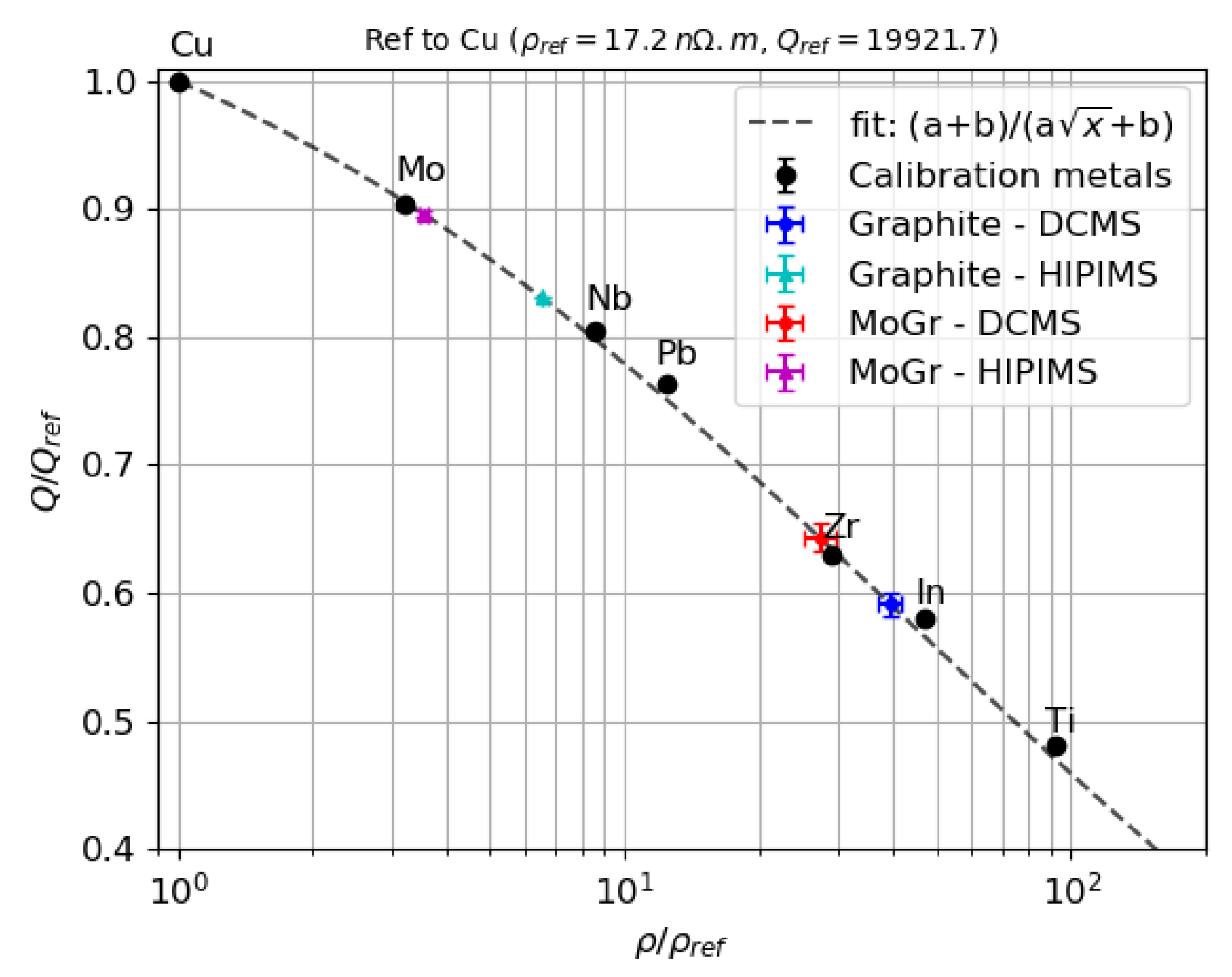
Figure 22.
Measured Q variation for Mo coatings on MoGr and graphite substrates obtained with HIPIMS and DCMS. The reference material is copper, nΩm, with .
Figure 22.
Measured Q variation for Mo coatings on MoGr and graphite substrates obtained with HIPIMS and DCMS. The reference material is copper, nΩm, with .
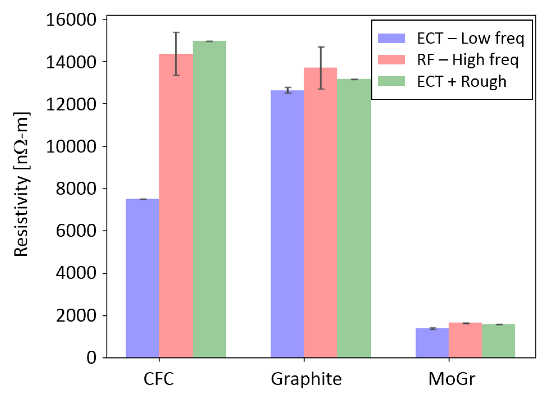
Figure 23.
Measured resistivity with low-frequency ECT (purple bar) and high frequency RF (red bar) techniques compared with the resistivity obtained with ECT accounting for surface roughness with the gradient model (green bar).
Figure 23.
Measured resistivity with low-frequency ECT (purple bar) and high frequency RF (red bar) techniques compared with the resistivity obtained with ECT accounting for surface roughness with the gradient model (green bar).
Figure 24.
SEM observations of a Mo-coated MoGr sample produced with DCMS. The fracture surface (bottom) and the coating surface (top) are shown.
Figure 24.
SEM observations of a Mo-coated MoGr sample produced with DCMS. The fracture surface (bottom) and the coating surface (top) are shown.
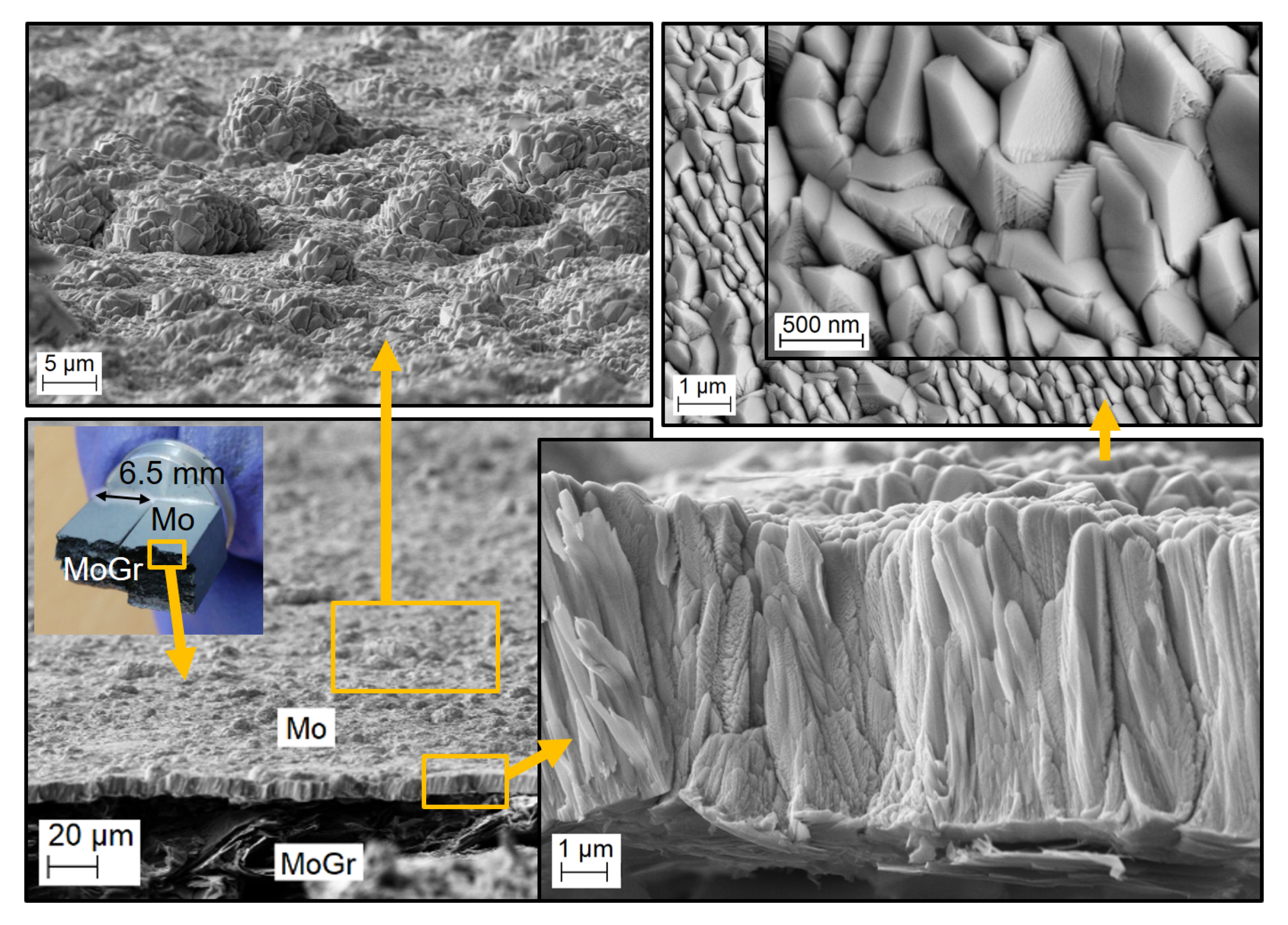
Figure 25.
SEM observations of a Mo-coated MoGr sample produced with HIPIMS. The fracture surface (bottom) and the coating surface (top) are shown.
Figure 25.
SEM observations of a Mo-coated MoGr sample produced with HIPIMS. The fracture surface (bottom) and the coating surface (top) are shown.
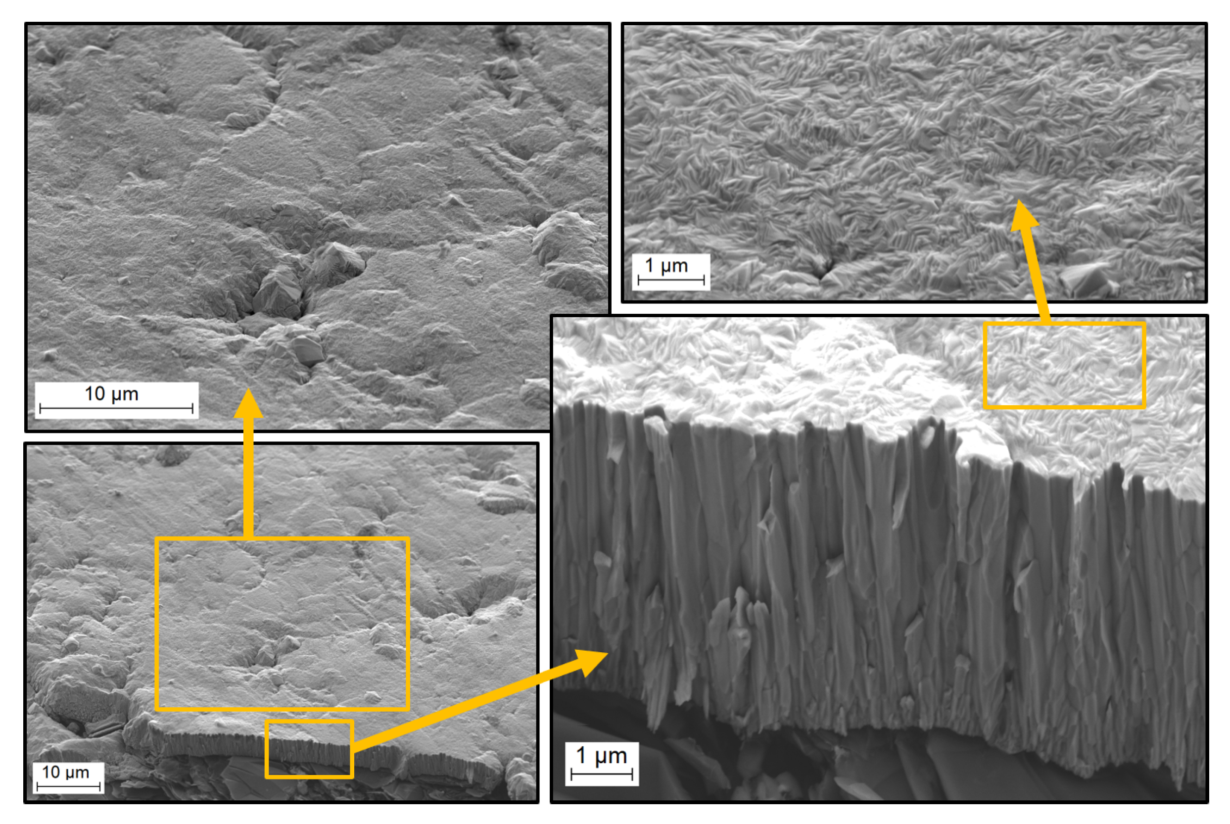
Figure 26.
SEM observations of a Mo-coated graphite sample produced with DCMS. The fracture surface (bottom) and the coating surface (top) are shown.
Figure 26.
SEM observations of a Mo-coated graphite sample produced with DCMS. The fracture surface (bottom) and the coating surface (top) are shown.
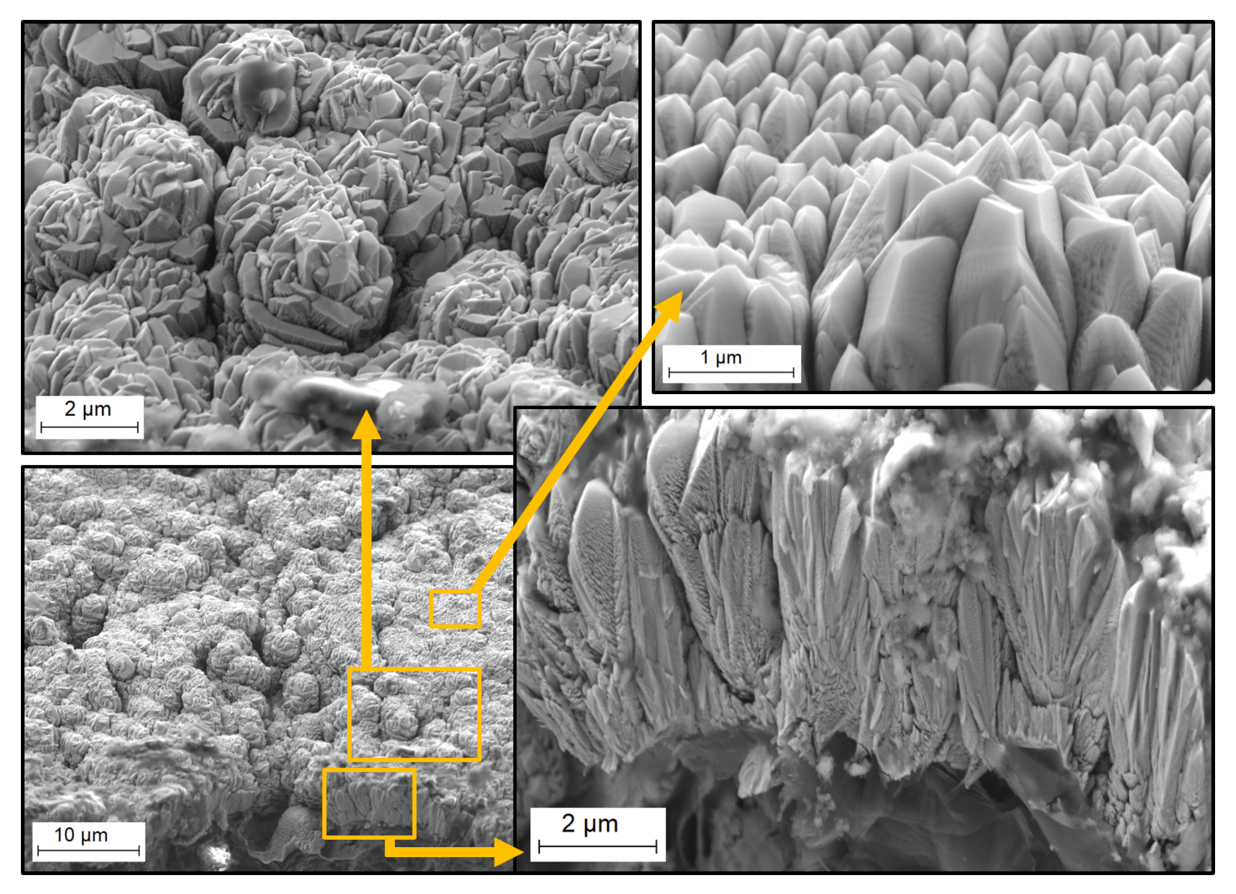
Figure 27.
SEM observations of a Mo-coated graphite sample produced with HIPIMS. The fracture surface (B) and the coating surface (top) are shown.
Figure 27.
SEM observations of a Mo-coated graphite sample produced with HIPIMS. The fracture surface (B) and the coating surface (top) are shown.
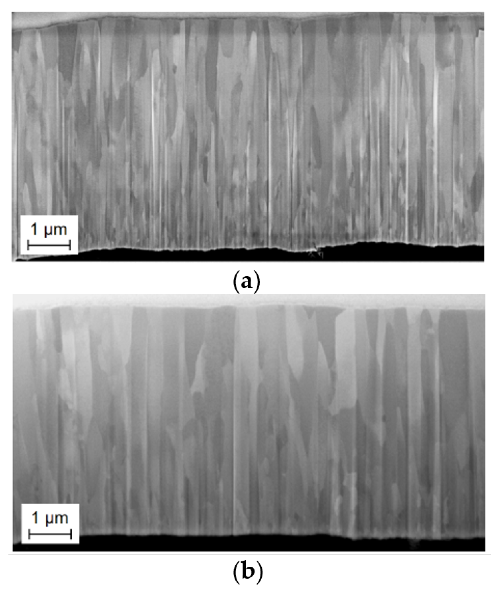
Figure 28.
FIB cross-sections on Mo-coated samples produced on graphite (a) and on MoGr (b) substrates with HIPIMS. The contrast between grains is due to the electron channeling effect. Vertical lines are due to the FIB process.
Figure 28.
FIB cross-sections on Mo-coated samples produced on graphite (a) and on MoGr (b) substrates with HIPIMS. The contrast between grains is due to the electron channeling effect. Vertical lines are due to the FIB process.
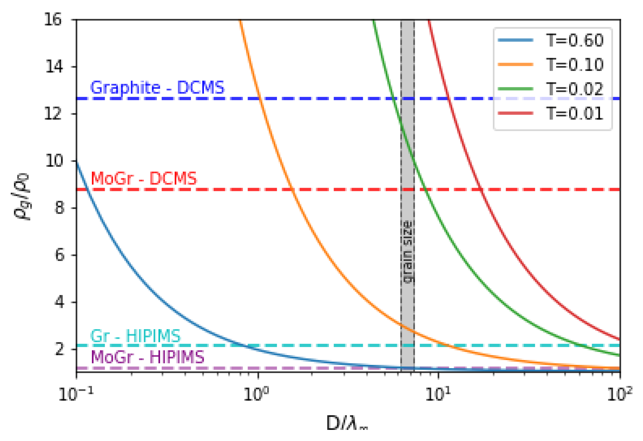
Figure 29.
Relative change in resistivity with respect to the ratio of grain size
D and mean free path
for Mo coating layers. Full lines correspond to different transmission
T between grain boundaries. Dashed lines correspond to the mean RF values of
Table 7.
Figure 29.
Relative change in resistivity with respect to the ratio of grain size
D and mean free path
for Mo coating layers. Full lines correspond to different transmission
T between grain boundaries. Dashed lines correspond to the mean RF values of
Table 7.
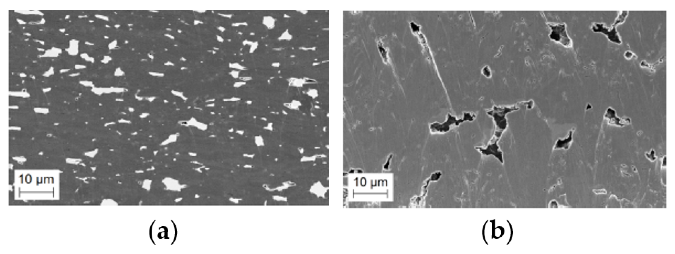
Figure 30.
SEM observations of ion-polished MoGr (a) and graphite (b) substrates. MoGr has its through-plane direction perpendicular to the image. Large μm-scale voids are visible on graphite (holes in black), while Mo-carbide inclusions are visible on MoGr (white spots).
Figure 30.
SEM observations of ion-polished MoGr (a) and graphite (b) substrates. MoGr has its through-plane direction perpendicular to the image. Large μm-scale voids are visible on graphite (holes in black), while Mo-carbide inclusions are visible on MoGr (white spots).
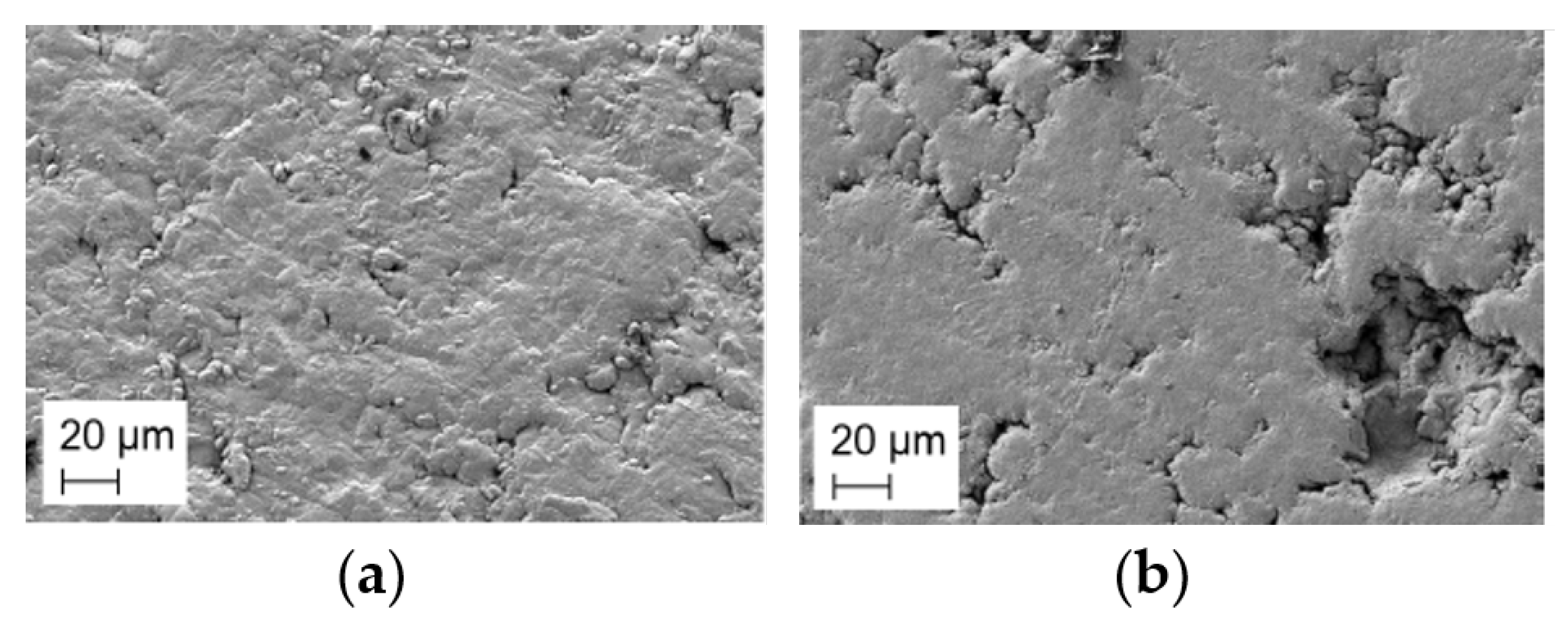
Figure 31.
SEM observations of Mo coating produced with HIPIMS on MoGr (a) and graphite (b). Note how the coating replicates the substrate features, producing discontinuities.
Figure 31.
SEM observations of Mo coating produced with HIPIMS on MoGr (a) and graphite (b). Note how the coating replicates the substrate features, producing discontinuities.
Table 1.
LHC design, LHC Run 2 and HL-LHC parameters for the most critical beam (BCMS [
14]).
Table 1.
LHC design, LHC Run 2 and HL-LHC parameters for the most critical beam (BCMS [
14]).
| | LHC | |
|---|
| Parameter | Design | Run 2 | HL-LHC |
|---|
| Beam energy (TeV) | 7 | 6.5 | 7 |
| Bunch intensity (p) | | | |
| Number of bunches | 2808 | 2556 | 2748 |
| Normalized emittance | 3.5 μm | 2.5 μm | 2.1 μm |
Table 2.
Summary of CFC, graphite, MoGr and Mo electrical resistivity at DC assumed in beam stability computations (for anisotropic materials the resistivity is considered on the beam direction).
Table 2.
Summary of CFC, graphite, MoGr and Mo electrical resistivity at DC assumed in beam stability computations (for anisotropic materials the resistivity is considered on the beam direction).
| Material | CFC | Graphite | MoGr | Mo |
|---|
| [nΩm] | 5000 [22] | 13,000 [21] | 1390 | 53.4 [23] |
Table 3.
Electrical resistivity of CFC, graphite and MoGr measured with the four-probe method on thick samples. X, Y, Z subscripts represent the 3 orthotropic directions of the materials (only graphite is isotropic).
Table 3.
Electrical resistivity of CFC, graphite and MoGr measured with the four-probe method on thick samples. X, Y, Z subscripts represent the 3 orthotropic directions of the materials (only graphite is isotropic).
| Material | (nΩm) | (nΩm) | (nΩm) |
|---|
| CFC | 32,600 | 8200 | 5700 |
| Graphite | 12,600 | 12,600 | 12,600 |
| MoGr | 14,200 | 1390 | 1390 |
Table 4.
Ratio of Mo coating to MoGr bulk resistance in function of the bulk thickness. The MoGr resistivity considered is shown in
Table 3.
Table 4.
Ratio of Mo coating to MoGr bulk resistance in function of the bulk thickness. The MoGr resistivity considered is shown in
Table 3.
| Thickness (mm) | (mΩ) | |
|---|
| 5 | 0.28 | 33 |
| 0.15 | 9.3 | 1 |
Table 5.
Resistivity of CFC, graphite and MoGr measured with the four-probes method on thin samples.
Table 5.
Resistivity of CFC, graphite and MoGr measured with the four-probes method on thin samples.
| Material | CFC | Graphite | MoGr |
|---|
| (nΩm) | 9900 ± 3000 | 9900 ± 3100 | 1240 ± 330 |
Table 6.
In-plane electrical resistivity of CFC, graphite and MoGr measured with the ECT.
Table 6.
In-plane electrical resistivity of CFC, graphite and MoGr measured with the ECT.
| Material | CFC | Graphite | MoGr |
|---|
| (nΩm) | 7497 ± 13 | 12,640 ± 130 | 1380 ± 30 |
Table 7.
Resistivity (in nΩm) measured with the DC, ECT and RF techniques for DCMS and HIPIMS Mo coatings on MoGr or graphite substrates.
Table 7.
Resistivity (in nΩm) measured with the DC, ECT and RF techniques for DCMS and HIPIMS Mo coatings on MoGr or graphite substrates.
| Bulk | Mo Coating | DC | ECT | RF |
|---|
| MoGr | DCMS | | | |
| HIPIMS | | | |
| Graphite | DCMS | | | |
| HIPIMS | | | |
Table 8.
In-plane electrical resistivity of CFC, graphite and MoGr measured with the resonant cavity, together with roughness
parameter [
41].
Table 8.
In-plane electrical resistivity of CFC, graphite and MoGr measured with the resonant cavity, together with roughness
parameter [
41].
| Material | (nΩm) | Typical (μm) |
|---|
| CFC | 14,400 ± 1000 | 9.4 |
| Graphite | 13,700 ± 1100 | 1.4 |
| MoGr | 2170 ± 140 | 1.1 |
Table 9.
In-plane grain size of the coating cross-sections (average ± standard deviation) from image analysis of
Figure 28.
Table 9.
In-plane grain size of the coating cross-sections (average ± standard deviation) from image analysis of
Figure 28.
| Location | on MoGr (μm) | on Graphite (μm) |
|---|
| Coating surface | | |
| Coating mid-thickness | | |

 ,
, 


