1. Introduction
A copper interconnect in advanced microelectronic devices conventionally uses a sputter-deposited Ta/TaN barrier layer to promote the adhesion and block diffusion of Cu into underlying materials. The Cu interconnect is typically fabricated by the damascene process. The process includes the sputter deposition of the Ta/TaN barrier layer and Cu seed layer, followed by filling trenches/vias using electrochemical deposition of Cu. As the feather size of microelectronic devices further shrinks, the fabrication of the Cu interconnects into a nano-scaled device is difficult due to the non-conformal deposition of the ordinarily sputtered Ta/TaN barrier and the Cu seeds. The non-conformal deposition reduces the sidewall space on the trenches/vias, limiting the following gap-fill capability of Cu electrochemical deposition. Thus, deposition of the film through an atomically precise methodology is essential for applications in the nano-scaled devices.
Cu alloy thin films as a self-forming barrier/seed have received much attention because the alloy film can replace the conventional Ta/TaN barrier and Cu seed [
1,
2]. The self-forming Cu alloy films doped with an element can retard the detrimental reactions between Cu and Si and further improve resistance to electromigration [
3,
4,
5]. Furthermore, the use of a self-forming Cu alloy film reduces the overall electrical resistivity of Cu interconnects, because it avoids the use of the high-resistive Ta/TaN barrier layer [
1]. Cu(Mn) film has appeared to be the most promising self-forming Cu alloy materials for future interconnects [
2,
6,
7,
8,
9,
10,
11,
12,
13]. However, the studied self-forming Cu(Mn) films are normally deposited by the sputtering process, and the sputtering process also impedes the film gap-filling capability in the high-aspect-ratio trenches/vias. Thus, developing a methodology capable of conformal deposition of the self-forming Cu(Mn) film is essential for the implementation of future interconnects.
Currently, the Cu interconnects that were used in microelectronics are normally deposited by an electrochemical deposition on the Ta/TaN barrier and Cu seed stacked layers [
14,
15]. Recent progress shows that the vacuum-based atomic layer deposition is capable of gap-filling in high-aspect-ratio trenches/vias. However, the literature on the electrochemical deposition of Cu(Mn) alloy thin film is rare, particularly for application to microelectronic devices, because Mn has a low, negative reductive potential (
E0 (Mn
2+/Mn) = −1.18 V
SHE) [
16,
17,
18]. To tackle this issue, we have reported that the Cu(Mn) film can be electrochemically deposited through a sequence of surface-limited redox replacement (SLRR) of Cu to replace the previous sacrificial, underpotentially deposited (UPD) Pb and inserting a UPD-Mn [
19]. In this method, the concentration of the Cu(Mn) film can also be adjusted by alternating Cu/Mn deposition cycle ratios.
In this study, we propose an electrochemical layer-by-layer deposition methodology that can fabricate Cu interconnects using whole wet processing. As shown, previous studies used the UPD-Pb as the sacrificial monolayer. Pb solution is known to cause environmental issues and affect biological systems. Thus, this study further presents an electrochemical deposition of Cu(Mn) film deposited using a UPD of Mn, without the use of the Pb sacrificial atomic layer, to mediate the growth of the films through the subsequent SLRR of Cu by replacing part of the UPD-Mn adatoms. Owing to the fact that the standard reductive potential of Cu is more positive than that of Mn, the UPD-Mn adatoms deposited on the substrate can be exchanged by the Cu
2+ ion in the following Cu electrolyte when the circuit is disconnected, i.e., the open circuit potential (OCP). Through controlling the OCP time, the Cu
2+ in the electrolyte can only replace a portion of the UPD-Mn adatoms during the Cu-SLRR, hence controlling the concentration of the films. The process has been reported to successfully deposit Cu(Co) alloy films [
20]. In this study, we further extend the work on the UPD-Mn-mediated growth of the controlled concentration of Cu(Mn) film. The capability of the Cu(Mn) film to function as a self-forming barrier for maintaining thermal stability will be investigated and a preliminary evaluation for the gap-filling capability will be also performed. The proposed technique can bring renewed interest in the electrochemical deposition of Cu(Mn) film in a layer-by-layer manner for applications in Cu self-forming barriers.
2. Experimental Procedures
Cu(Mn) films were electrochemically deposited on Ru/Si(100) substrates. The thickness of the Ru deposited using a direct current sputtering was 10 nm. A three-electrode deposition cell was adopted in this study. The working electrode was the Ru/Si substrate, a gold wire was the auxiliary electrode, and an Ag/AgCl (BASi RE-6) was the reference electrode. The electrochemical deposition was performed using a potentiostat. Before the electrochemical process, the substrates were cleaned in a 10 mM HClO4 (Aldrich, St. Louis, MO, USA) to remove any contamination layer on the Ru/Si surface by cyclic voltammetry (CV) method at a scan rate of 10 mV/s from +500 to −1500 mV for one cycle.
To deposit the Cu(Mn) film, an Mn adlayer was first deposited via UPD at a potential of −800 mV, which was determined from the cyclic voltammetry scan of an Mn electrolyte with a scan rate of 10 mV/s. The Mn electrolyte was a solution containing 1 mM of MnSO4·H2O (Hayashi Pure Chemical, Osaka, Japan) and 1 mM of (NH4)2SO4 (Hayashi Pure Chemical). During the UPD process, the Mn electrolyte was pumped into the deposition cell. After that, the electrolyte was maintained for 60 s at −800 mV to form a UPD-Mn adlayer. Then, deionized water was pumped into the deposition cell to remove the existing Mn electrolyte in the cell. Afterwards, the Cu electrolyte was pumped into the deposition cell at OCP and the Cu-SLRR was allowed to occur by replacing the UPD-Mn for a controlled time of 20, 40, and 60 s, due to the standard potential values difference between Cu and Mn (E0 Cu/Cu2+ = +0.34 VSHE; E0 Mn/Mn2+ = −1.18 VSHE). The Cu electrolyte contains 2 mM of CuSO4·5H2O (Hayashi Pure Chemical) and 1.2 mM of C2H4(NH2)2 (Shimakyu’s Pure Chemical, Osaka, Japan). The Cu(Mn) films were then deposited by sequentially performing the UPD-Mn and the SLRR-Cu in the controlled OCP time for 50 cycles. NaOH (J.T. Baker, Phillipsburg, NJ, USA) was used to adjusted the pH value of the electrolyte. The pH values of the Mn solution were in between 6.0 and 8.0 and the pH value of the Cu solution was 5.0.
X-ray diffraction (XRD, AXS D8A25, Bruker, Billerica, MA, USA) with Cu Kα radiation was used to examine the crystalline structure of the film. The compositions of the resultant Cu(Mn) films were analyzed by an inductively coupled plasma mass spectrometry (ICP-MS, 7500ce, Agilent, Santa Clara, CA, USA). The electrical resistivity of the film was conducted by a standard four-point probe measurement. Surface morphology and a cross-sectional image of the films were examined by a field emission scanning electron microscope (FESEM, JSM-7500F, JEOL, Tokyo, Japan). The effectiveness of the Cu(Mn) alloy film as a barrier layer was evaluated by observing the stability of the Cu overlayer using an overall sheet-resistance measurement by annealing the Cu(Mn) films by a rapid thermal annealer (RTA, MILA-5000, ULVAC, Chigasaki, Japan), at an elevated temperature ranging from 400 to 600 °C, for 5 min in an Ar/H2 (5%) ambient.
3. Results and Discussion
The deposition potential, particularly for the UPD-Mn, is essential for the following SLRR-Cu because the layer-by-layer deposition process favors the UPD-Mn with an adlayer of the approximately atomic monolayer (ML). Thus, the reductive potential of the Mn deposition was first examined by a CV scan. As mentioned previously, the electrochemical deposition of Mn is difficult [
16,
17,
18]; the pH value affecting the redox properties of the Mn electrolyte was first elucidated because the pH value may affect the deposition of the resultant Mn adlayer.
Figure 1 exhibits the curves of the CV scans for the Mn electrolyte with different pH values ranging from 6.0 to 8.0. In the CV scans, the applied potentials sweep linearly from an initial potential of 0 mV to a negative potential of −1500 mV and back to a positive potential of +500 mV. After that, to finish the CV scans, the potential applied during the CV scans back to the initial potential of 0 mV. As seen from the CV curves, the current density for the Mn electrolytes with the studied pH values remains stable at a potential from 0 to −700 mV, followed by a significant increase in the current density at a potential higher than −700 mV. No obvious reductive potential of Mn was found during the CV scans, which is consistent with previous studies [
21,
22]. The subtle reductive potential might be attributed to the counteraction of the high reductive current density that arose from the hydrogen generation. As also seen from the CV curves, reductive current density increases with the increasing pH values. At pH = 8.0, however, the formation of Mn(OH)
2 causes a decline in the reductive current density because Mn
2+ may react with OH
− in the electrolyte [
23]. Thus, the electrolyte with a pH value of 7.5 was selected for the UPD-Mn deposition. A total of −800 mV was selected as the deposition potential of the UPD-Mn for the following Cu-SLRR through the proposed scheme for the electrochemical deposition of Cu(Mn) films.
To determine the terminated time of OCP during the Cu-SLRR for the deposition of Cu(Mn) film, the potential transient during the replacement between Cu
2+ and the UPD-Mn adatoms was evaluated.
Figure 2 shows the time–potential–current transient curves for the first 5 cycles of the UPD-Mn followed by the respective Cu-SLRR. In a cycle scheme, the UPD-Mn was first deposited on the Ru/Si substrate in the Mn electrolyte at the potential of −800 mV for 60 s. Then, the deionized water was used to remove the existing Mn electrolyte in the deposition cell. Afterward, the Cu electrolyte was introduced into the cell, and the auxiliary electrode was then disconnected to allow the working electrode to switch to its OCP. In this stage, the potential in the Cu electrolyte gradually shifted from −60 mV to a positive potential of ~ +175 mV over the next 300 s for the Cu-SLRR, as seen in
Figure 2. In this Cu-SLRR process, Cu
2+ ions moved to the substrate surface, replaced the UPD-Mn adatoms, and formed a Cu adlayer because of the standard potential difference between Mn and Cu. Simultaneously, the Mn adatoms replaced were transformed into Mn
2+ ions, dissolving into the Cu electrolyte. This replacement process induces that the negative potential in the initial stage of the Cu-SLRR gradually shifts toward positive, and the potential becomes stable at the equilibrium potential between the Cu
2+/Cu, when the replacement is completed at approximately 100 s.
The amount of UPD-Mn adatoms exchanged by the Cu2+ ions during the Cu-SLRR process was closely related to the OCP time, because the potential sharply increased in the first 60 s. This observation indicates that the amount of the UPD-Mn adatoms replaced by the Cu2+ ions can be adjusted by terminating the Cu-SLRR at a certain OCP time. The controlled OCP time means that the Cu2+ in the electrolyte only replaces a portion of the UPD-Mn adatoms and forms a controlled concentration in the resultant Cu(Mn) layer. A longer OCP time causes greater replacement, so as to yield a Cu(Mn) film with a higher Cu concentration. Because the potential changed rapidly in the first 60 s, the 60, 40, and 20 s were selected as the terminated OCP time to form the Cu(Mn) films.
The current density–time transient curve during the Mn-UPD was used to determine the coverage of the UPD-Mn deposited at −800 mV.
Figure 3 shows the measured transient curves of current density versus time that were recorded during the UPD of Mn, followed by the different terminated OCP times (i.e., 60, 40, and 20 s) of the Cu-SLRR. Initially, as shown, the current density dramatically increases to a negative value and then reaches a maximum negative value. In this stage, the applied UPD-Mn potential causes the reduction in Mn
2+ and forms an Mn adlayer on the substrate. Subsequently, the current density decreases gradually until reaching a stable value, indicating that the UPD of Mn has been terminated due to the UPD occurring at potentials prior to the potential for bulk deposition. The transient current densities were recorded at the different deposition cycles, as shown in
Figure 3a–c, followed by the Cu
2+ partially replacing the UPD-Mn at different terminated OCP times of 60, 40, and 20 s, respectively. Integration of the current density–time transient curves could provide the deposition charge of the UPD-Mn for the respective terminated OCP time. The deposition charges (
Q) are summarized in
Table 1. These charges were divided by two, owing to two electrons being transferred when one Mn adatom was substituted by one Cu
2+ ion. Additionally, the formation of one Mn monolayer requires a charge of 351 μC·cm
−2 [
24]. Thus, the respective charge obtained yields the coverage of the UPD-Mn. The resultant UPD-Mn coverage is in the range of 1.14 and 0.84 ML. The obtained coverage confirms the UPD-Mn, which is approximately a monolayer because the UPD occurs prior to the formal reductive potential. The UPD-Mn coverage decreases with decreasing terminated OCP time. This is because the shorter OCP time causes more UPD-Mn adatoms to remain on the substrate. The remaining UPD-Mn adatoms can thus partially retard the subsequent cycle of UPD-Mn deposition.
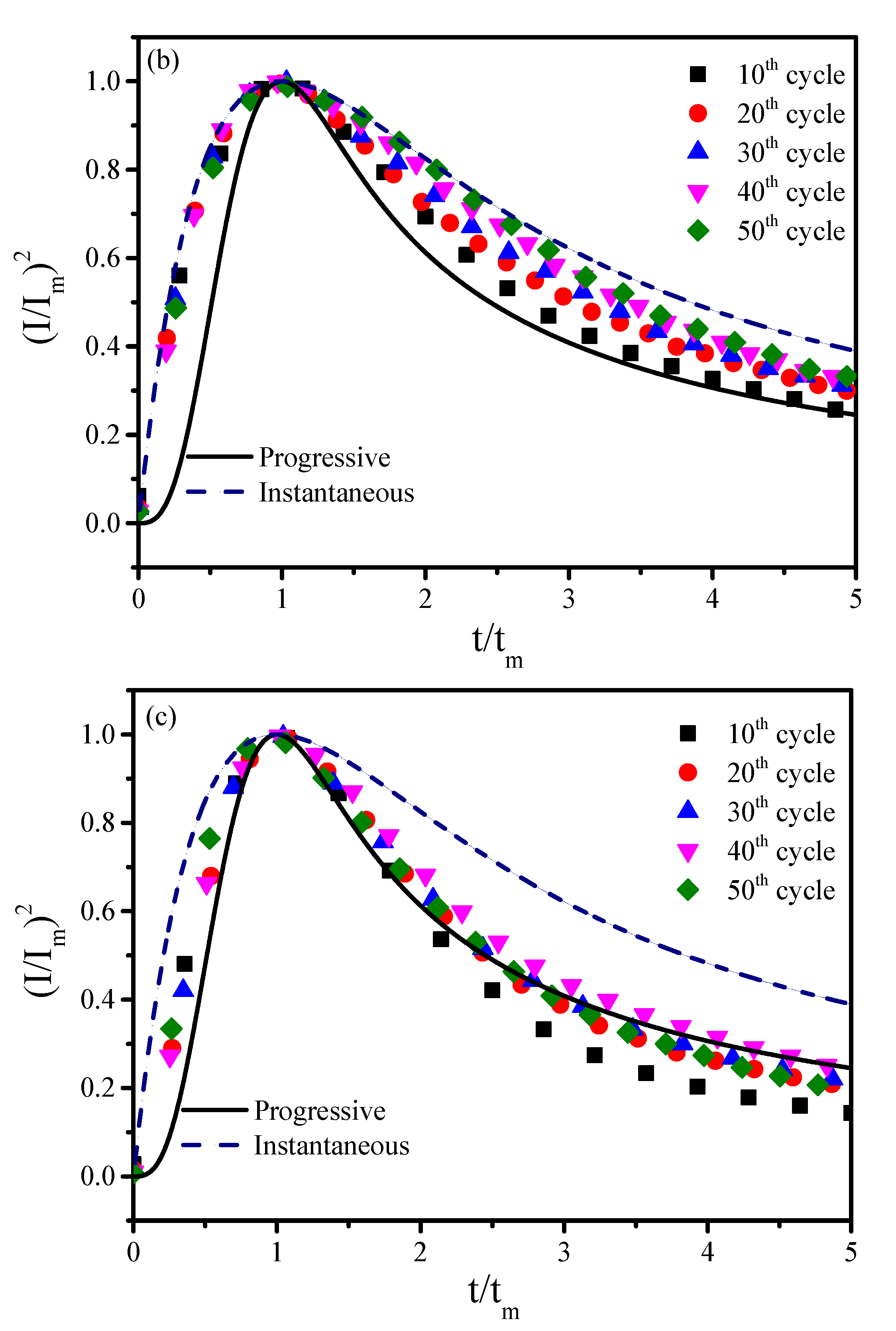
(
I/
Im)
2 vs.
t/
tm curves transformed from the current–time curves, where
I and
t are current and time and
Im and
tm are the current and the time at the respective peak coordinates, can be used to depict the nucleation mechanism [
25,
26,
27]. The (
I/
Im)
2 vs.
t/
tm curves with the various terminated OCP times for the Cu-SLRR are shown in
Figure 4. In this mechanism, nucleation can be described in terms of two limiting cases as follows: (a) progressive nucleation (solid curve) implies that the nucleation rate is slow and nucleation continues to occur on the surface while the existing nuclei are growing; (b) instantaneous nucleation (dotted line) indicates that nucleation rate is fast, so the nuclei are formed on the surface simultaneously within a short time.
Figure 4a shows that the nucleation conforms to the instantaneous nucleation for the 60 s-terminated OCP time. This is because more Cu
2+ can replace most of the existing UPD-Mn adatoms for the longer OCP time. The formation of SLRR-Cu can readily provide the nucleation sites for the next cycle deposition of UPD-Mn. This abundant nucleation sites thus form a uniform grain because almost all nuclei are formed simultaneously at the initial stage of the deposition, as surface morphology shows in
Figure 5a. Shortening the terminated OCP time to 40 s shows that the nucleation process is between the progressive and the instantaneous nucleation, as shown in
Figure 4b. In this process, part of the UPD-Mn adatoms still exists on the substrate for the 40 s OCP time. The subsequent Mn-UPD cycle thus induces an incomplete UPD-Mn, meaning the grain size of the resultant film is uneven, with a grain size ranging from 50 to 74 nm, as shown in
Figure 5b. Shorten the terminated OCP time to 20 s and the nucleation of UPD-Mn follows the progressive nucleation, as shown in
Figure 4c. The Cu(Mn) film has a small but less uniform grain (ranges from 50 to 80 nm) with moderate area density when the terminated OCP time is 20 s, as shown in
Figure 5c. This implies that the nuclei nucleation is dominated by the progressive nucleation, in which nuclei both grow at their former positions and nucleate on newly activated nuclei [
28].
Figure 6 presents the XRD patterns of the Cu(Mn) films that were deposited at their respective terminated OCP times during the Cu-SLRR. All samples have Cu(111) diffractions (2θ = 43.2°, JCPDS 89-2838) and their peak intensity increases with increasing terminated OCP time. This fact supports that the longer OCP time enables greater replacement between the Cu
2+ and UPD-Mn and tends to yield a Cu(Mn) film with a higher Cu concentration. The Cu(111) orientation can extend the use of Cu(Mn) in the Cu interconnects because the (111) orientation has a low strain energy and surface energy [
29,
30]. However, a peak corresponding to the Cu
2O (111) (2θ = 36.7°) and (200) (2θ = 42.5°) (JCPDS 78-2076) was also found in the XRD pattern because Cu
2+ might react with the residual oxygen in the electrolyte, because oxygen is inevitable although the deionized water has been previously degassed by bubbling high-purity nitrogen. Suitable trisodium citrate can inhibit the formation of Cu
2O because the citrate ions can complex oxygen ions [
31]. However, no Mn and Mn oxides peaks appeared, suggesting that the Mn segregation may too low to be detected in the as-deposited state [
32].
ICP-MS analysis of the as-deposited films was used to examine the film composition.
Table 2 shows the composition of the studied Cu(Mn) films. The obtained composition depicts that the concentration of Mn in the Cu(Mn) film increases with decreasing OCP time. As shown, the shorter OCP time causes less replacement and results in a higher Mn concentration in the Cu(Mn) film. Thus, the concentration of the Cu(Mn) film can be controlled by manipulating the OCP time during the SLRR process through this scheme. The Cu(Mn) film can also be successfully electrochemically deposited through controlling the OCP time during the Cu-SLRR. This process can use the sequence of surface-limited redox replacement (SLRR) of Cu to replace the sacrificial underpotentially-deposited (UPD) Pb and insert an UPD-Mn [
19].
Table 2 also shows the electrical resistivity vs. respective terminated OCP time for the as-deposited Cu(Mn) films. The electrical resistivity of the as-deposited film decreases with the increasing terminated OCP time and reaches a low electrical resistivity of 18.1 μΩ·cm for the film with an OCP time of 60 s. Cu(Mn) films may form an alloy compound through the corresponding UPD-Mn and SLRR-Cu. The remaining Mn element in the Cu(Mn) film thus acts as an impurity. The increased Mn addition provides more electron-scattering centers in the conduction process. Thus, the longer OCP time enables the Cu
2+ to replace more UPD-Mn and decreases the electrical resistivity of the Cu(Mn) film. As mentioned, the Cu(Mn) film, deposited in an electrochemical manner, is rare. Our previous study has shown that the lowest electrical resistivities of 44.4 μΩ·cm for the as-deposited Cu(Mn) film that was electrochemically deposited resulted in an Mn concentration at approximately 10.0 at.% [
19]. Annealing can cause a decrease in the electrical resistivity of Cu(Mn) films, in particular for the film with 60 s OCP, which will be discussed in the following section. The electrical resistivity of the as-deposited Cu(Mn) film in this study is consistent with the previously obtained values from the literature, depending on the Mn concentration and the deposition technique that was used [
19,
33,
34].
Figure 7 shows the changes in electrical resistivity for the annealed Cu(Mn) films that were deposited at the respective terminated OCP time. Examining the change in the electrical resistivity can help to estimate the degree of intermixing between the Cu(Mn) film and the substrate. The electrical resistivity of Cu(Mn) films reduces due to the grain growth when the samples were annealed at an elevated temperature below 500 °C, indicating that all of the Cu(Mn) films were thermally stable and no reaction occurred between the Cu(Mn) films and the substrate. However, the electrical resistivity abruptly increases at 600 °C for the terminated OCP time of 20 s (the Cu(Mn) with 12.05% Mn), indicating that the film has agglomerated and/or intermixed with the substrate. However, the Cu(Mn) film with a terminated OCP time above 40 s still remains stable at 600 °C. The results have shown that the studied Cu(Mn) films are thermally stable at least up to 600 °C. The surface morphologies of the annealed Cu(Mn) films were shown in the inset in
Figure 7. Notably, the electrical resistivity of the Cu(Mn) film deposited at the terminated OCP time of 60 s reaches 7.0 μΩ·cm when the film was annealed at 500 °C. As is generally agreed, a thin film with a nanometer thickness can lead to a remarkable increase in electrical resistivity. A survey of the literature showed that a 50 nm thick Cu film prepared by electrodeposition has an electrical resistivity of 8.2–12.0 μΩ·cm [
35]. The Cu(Mn) film in this study has a slightly lower electrical resistivity compared with the typical electrical resistivity obtained from the electrodeposition, implying that the proposed technique is essential for the implementation of future Cu interconnects.
The sharp increase in the electrical resistivity of the Cu(Mn) films is attributed to the intermixing between the Cu(Mn) and Ru/Si substrate and/or grain agglomeration itself when the film was annealed at an elevated temperature. Structural changes examined by XRD for the studied Cu(Mn) films, annealed at 600 °C, were shown in
Figure 8. Only a Cu(111) diffraction peak appeared, accompanied by a tiny peak in the underlying Ru/Si substrate when the Cu(Mn) film for 60 s-OCP was annealed at 600 °C. This fact reveals that the Cu(Mn) film with 60 s OCP is thermally stable at 600 °C. This is consistent with the results shown in
Figure 7. However, the Cu(Mn) films for 40 s and 20 s OCP exhibit a Cu
3Si diffraction peak, indicating that intermixing has occurred. Note that the 40 s-OCP Cu(Mn) film still had a low electrical resistivity when the film was annealed at 600 °C (
Figure 7). This is because the Cu(Mn) film remained continuous and carried almost all of the probe current, although tiny Cu
3Si appeared on the surface. Accordingly, the formation of Cu
3Si may not be instantly disclosed via the electrical resistivity measurement.
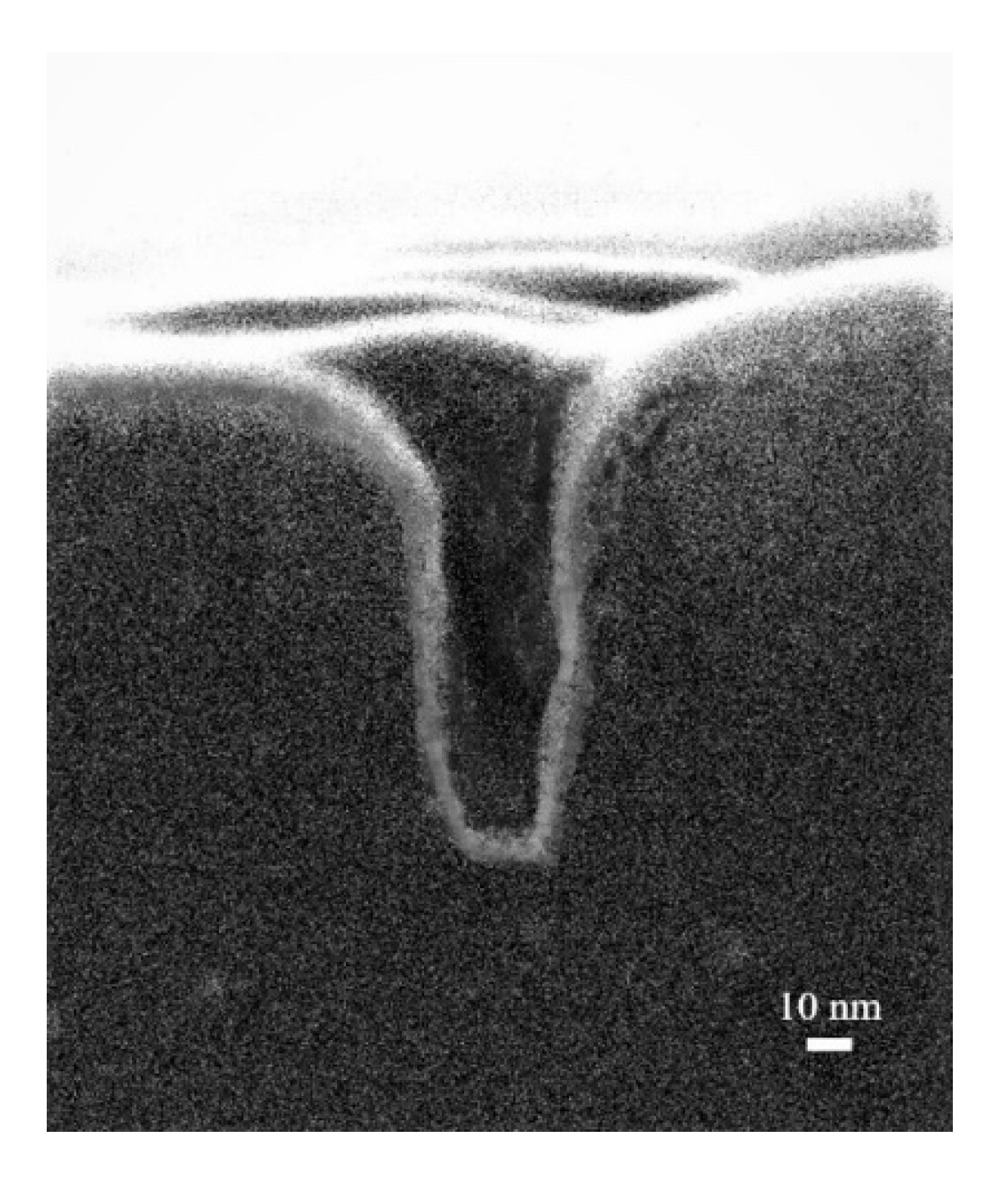
Preliminary cross-sectional SEM analysis indicates that Cu
2+ replaces the UPD-Mn for the OCP time of 60 s developed here, and is capable of depositing a conformal Cu(Mn) into narrow holes with an aspect ratio of 5 (depth of 100 nm and width of 20 nm), as shown in
Figure 9. In general, the conformal deposition indicates the capability of the thin film deposition process to deposit on the top surface as well as the bottom and sidewall surface of a trench/hole. The calculated sidewall step coverage is 0.50; the ratio of film thickness on the sidewall of the hole to that on the top surface and the bottom step coverage is 0.81; the ratio of film thickness on the bottom of the hole to that on the top surface shows no observable overhang. The greater bottom step coverage suggests that film grows primarily in a manner of bottom-up filling.


