Article

Fabrication of a Thick Crystalline Al2O3 Coating with Insulation and High Thermal Conductivity via Anodic Oxidation and Subsequent Mic Arc Discharge Treatment

1
Faculty of Materials Science and Engineering, Xi’an University of Technology, NO.5 South Jinhua Road, Xi’an 710048, China
2
School of biological and Chemical Engineering, Nanyang Institute of Technology, NO.80 Changjiang Road, Nanyang 473004, China
*
Author to whom correspondence should be addressed.
Coatings 2020, 10(1), 38; https://doi.org/10.3390/coatings10010038
Submission received: 20 November 2019 / Revised: 18 December 2019 / Accepted: 23 December 2019 / Published: 1 January 2020
(This article belongs to the Special Issue Surface Plasma Treatments)

Abstract

:
Amorphous Al2O3 coating with a thickness of 143 μm was firstly prepared by anodic oxidation, then the amorphous Al2O3 was transformed into crystalline Al2O3 through applying micro arc discharge. The crystal structure of the Al2O3 coatings was analyzed with an X-ray diffractometer. Results indicated that the coating consisted of amorphous and crystalline Al2O3. The microstructure of the coating was characterized by scanning electron microscopy, which showed that the coating had a compact structure. The thermal conductivity of the coating was 23.7 W/m·K, which is significantly higher than that of amorphous Al2O3 coating. The total and specific breakdown voltages of the coating were 3.85 kV and 26.92 kV/mm, which is suitable to apply for high power LED heat sink substrate.

1. Introduction

Aluminium based materials, have received great attention in the electronic industry, especially in the heat sink substrate of light emitting diode (LED) lamps [1,2,3], due to their advantages of high specific strength, proper corrosion resistance, as well as sound thermal conductivity. Typically, an LED heat sink substrate consists of three layers: aluminum alloy at the bottom, a copper circuit in the top, and various organic compounds have been used as middle layers to ensure insulation between them [4]. Nonetheless, poor thermal emissivity decrease the thermal dissipation efficiency of radiation [5]. With the rapid development of LED lamps to high power, high light intensity and small volume, heat dissipation has become an essential challenge [6]. To increase the power of LED lamp from 0.35 W to 1 W and reduce its volume, the insulation of the LED lamp should increase from 2 to 3 kV, the thermal conductivity should increase from 2 W/m·K to 15 W/m·K.
The thermal resistance formula [7] of multilayer structure is as follow:
R = δ 1 R 1 + δ 2 R 2 + δ 3 R 3
where R and δ represent the thermal resistance and thickness of each layer respectively. The insulation and thermal conductivity of different materials were shown in Table 1. As the thermal conductivity of the insulation layer is much lower than substrate and copper layer, according to Equation (1), enhancing thermal conductivity while maintaining the insulation of the insulation layer has become a key technology in the LED industry [8].
Many coating materials, such as silica, insulation gasket, insulation adhesive, insulation grease can be used to ensure the insulation requirement of aluminum alloy substrate, but they cannot be used on the heat sink with special size (such as thin strip). Furthermore, their low dielectric strength and thermal conductivity (seen in Table 1) limited the application on high power electronic devices. Preparing aluminum nitride or alumina coating on the substrate can enhance the heat dissipation efficiency of the substrate [17]. Although aluminum nitride coating can provide higher thermal conductivity, its dielectric strength is 8 kV/mm, while its thickness is difficult to exceed 5 μm, and the coating size is limited to less than 4.5 square inches. When compared with aluminum nitride coating, the preparation cost of alumina coating is lower and can be coated on a large-size substrate [18]. Even though its theoretical thermal conductivity is 1/5–1/8 of that of aluminum nitride coating (seen in Table 1), the thermal conductivity is close to aluminum nitride coating in practical application. As the dielectric strength of alumina coating is five times higher than that of aluminum nitride, the alumina coating is much thinner than aluminum nitride to achieve the same breakdown voltage. It is well known that enhancing the thermal conductivity or making the coating thickness thinner can improve the thermal performance of the insulation layer. Therefore, in the high power LED industry, it is an available method to prepare alumina coating on the substrate.
Utilizing the electrochemical method, a compact alumina coating can be obtained by anodizing [19] or micro arc oxidation (MAO) technology [20] in order to provide insulation for the substrate. The MAO technology can be adopted to obtain alumina ceramic coating on the substrate, which can provide excellent insulation as well as thermal conductivity simultaneously. For a high power LED, a high breakdown voltage (3 kV) requires the MAO coating thickness reach 75–136 microns. Nonetheless, there is much cavitation in the coating if the coating thickness exceeds 30 microns, paradoxically. Due to the existence of oxygen in MAO coating, the insulation and thermal conductivity of the coating decrease significantly [21]. A through-hole amorphous alumina coating with the thickness that reaches hundreds of microns [22] can be produced by anodizing technology. Unfortunately, the thermal conductivity is poor [23]. Restricted by thermodynamics, the phase transition temperature (1150 °C) of amorphous alumina to α-alumina is much higher than the liquefaction temperature (660 °C) of aluminum [24]. Thus, it cannot obtain a thick compact alumina ceramic coating by the heating method.
The anodizing of aluminum alloy is mainly carried out in acid electrolyte, and the reaction equation is as follows [25]:
Anode:    Al3+ + 3OHAl(OH)3 − 77.1kJ/mol
4OH + 4e → 2H2O + O2 − 46.6kJ/mol
2Al(OH)3Al2O3 + 3H2O + 194.6kJ/mol
Cathode:    2H+ + 2eH2
Due to the heat released by Equation (2) being lower than the heat required by the Equation (3), the anodic coating is mainly consisted of Al(OH)3, resulting in the insulation and thermal conductivity of anodic coating being far lower than MAO coating.
If the pre-anodic substrate(seen in Figure 1) is placed in a electrolyte tank, due to the impact of electric spark or plasma discharge, according to the Equation (4), the amorphous alumina can be transformed to alumina ceramic coating at room temperature [26] by the strong exothermic (center temperature of 7000 K) effect of in situ oxygen plasma ionization. With the crystal phase transformation of amorphous alumina, the amorphous alumina colloid shifts slightly to the aluminum alloy substrate under the effect of dehydration shrinkage force as well as oxygen bubble collapse force [27]. The through-hole of the anodic coating can be sealed, and a thick compact alumina ceramic coating can be obtained, meeting the requirements of high power LED on the insulation as well as thermal conductivity of substrate coating.
According to the types of acid, the electrolyte used in the process of anodizing can be divided into sulfuric acid, phosphate acid, chromic acid, oxalic acid and so on. The parameters of the micro-structure of the aluminum alloy anodic coating in different electrolytes are shown in Table 2.
It can be seen that the thickness of anodic coating obtained in sulfuric acid electrolyte reaches 200–400 microns, yet the aperture diameter is so small that the gas generated in the process of micro arc discharges cannot escape from the micropore, which prevents further micro arc discharges and the formation of alumina ceramic. As the alumina coating obtained in phosphoric acid electrolyte has appropriate aperture diameter to promote micro arc discharges, and the thickness is higher than that in chromic acid or oxalic acid electrolyte, if mixed sulfuric acid and phosphate acid serve as electrolyte, it is predictable to obtain an anodic coating with thickness and aperture diameter can meet the requirement of subsequent plasma discharge.
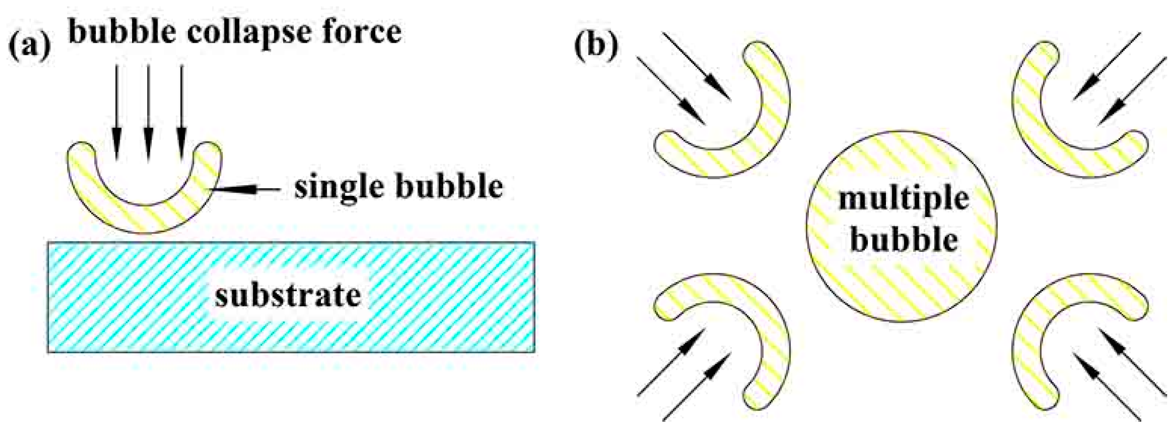
In the process of plasma discharge, according to Equation (3), the heat and oxygen was generated simultaneously. When the plasma discharge intensity was low, the number of oxygen bubbles was small and had no interaction between them occurred. The direction of bubble collapse force was perpendicular to the substrate. When the plasma discharge intensity was high, the number of oxygen bubbles increased and had strong interaction between them each other. The direction of bubble collapse force was parallel to the substrate (seen in Figure 2) [7]. As the plasma discharge intensity is effected by parameters such as current density, discharge time and duty cycle, the influence of above parameters on the coating performance were studied.
In this study, to meet the requirement of high power LED on the heat sink substrate, anodizing and MAO technology were combined. A thick anodic alumina coating was prepared in sulfuric-phosphoric acid electrolyte, and then the amorphous alumina coating was transformed to alumina ceramic in the condition of plasma discharge. The suitable anodizing, plasma discharge condition were studied. The thickness, crystalline phase composition, micro morphology and cross section of the coatings were characterized, the breakdown voltage and thermal conductivity of the coatings were tested and compared with those of the anodic and MAO coatings.

2. Experiment

2.1. Materials and Pre-treatment

Specimens with dimensions 20 × 20 × 5 mm3 of aluminium 6061 alloy (AA 6061) was adopted as substrates for anodizing. The composition of the alloy was shown in Table 3.
The specimens were mechanically ground with 240, 400 and 800 grit silicon carbide paper, and washed with distilled water. Prior to anodizing, the specimens were etched in 5 wt % NaOH solution at 60 °C for 3 min, chemical polished in 30 vol % HNO3 solution, and then dried in a cold air stream. Between different pre-treatment steps, the specimens were intensively washed with deionized water.

2.2. Preparation of Aluminum Alloy Oxidation Coatings

All the experimental reagent were purchased from Tianjin Kemiou chemical reagent Co. Ltd. Two 300 × 300 mm2 AISI 321 stainless steel sheets (BENLAIMETAL, Shanghai, China) were used as the cathode. To reduce Joule heat, a DC pulse supply was selected. The anodizing process of the AA 6061 specimens was undertaken at the current density of 50 mA/cm2, in a stirred speed of 60 r/min, at 4 °C for 80 min. The anodizing coatings were fabricated in a sulphuric and phosphoric acid electrolyte, and the parameters that change in each treatment process were shown in Table 4.
After the anodizing, the specimens were immediately washed with deionized water and were immersed in a stirred electrolyte consisting of 40 g/L (NaPO3)6, 10 g/L Na2B4O7·10H2O, 5 g/L NaOH, as well as 5 g/L citric acid. On the conditions of the DC pulse supply with the frequency of 20 kHz, the plasma discharge temperature at 20 °C, the parameters that change in each treatment process were shown in Table 5. To study the performance of the coating, two MAO coatings with the thickness of about 25 μm and 50 μm were prepared at the same supply and pre-treatment conditions. All the experiments were repeated three times.

2.3. Coating Characterization

The phases composition of different coatings was examined by an X-ray diffractometer (XRD) (D/max-rB, RICOH, Akishima-shi Tokyo, Japan) with a CuKα source. The accelerating voltage and applied current were 40 kV and 30 mA, respectively. The micro-structure of the coating surface and cross-section were studied by the scanning electron microscopy (SEM) (S-4700, Hitachi, Tokyo, Japan). Coating thicknesses produced at different conditions were measured using the eddy current coating thickness measurement gauge (CTG-10, Time Company, Shanghai, China). The thicknesses at 10 different places on the surface of the coating were measured, and the average thickness was calculated. The total breakdown voltage was tested by withstand voltage tester (AN 9636 HS: 500 VA, Ainuo Instrument Co. Ltd., Shanghai, China). The breakdown voltage at 10 different places on the surface of the coating were measured, and the average value was calculated. The specific breakdown voltage was calculated depending on the ratio of average breakdown voltage to average thickness. The thermal conductivity was tested by heat conduction coefficient measurement device (TC 3000E, XIATECH Electronic Technology Co., Ltd., Xi’an, China) with the test temperature 25 °C and the duration time 0.9–1.2 s.

3. Results and Discussion

3.1. Thickness of Anodic Coating

Figure 3a indicates the influence of sulfuric acid and phosphoric acid concentration on the thickness of anodic coating, with the decreasing of sulfuric acid concentration, the coating thickness increased, and the uniformity of coating thickness decreased [32,33]. When the concentration of sulfuric acid was reduced to 55 g/L, the thickness of the coating is 143 μm and continued to reduce the sulfuric acid concentration, the coating thickness was so inhomogeneous that it was not conductive to subsequent micro arc discharge. Therefore, the concentration of sulfuric acid was determined to be 55 g/L. The influence of phosphoric acid concentration on the thickness and uniformity of the coating was also studied and illustrated in Figure 3b, it can be seen that with the addition of phosphoric acid, the thickness and uniformity of the coating decreased obviously, yet the apertures of the anodic coating increase. When the concentration of phosphoric acid was 9.5 g/L, the aperture diameter of anodized coating was too small to initiate micro arc discharge. When the concentration of phosphoric acid was 28.5 g/L, the thickness inhomogeneity of anodic coating soared. When the concentration of the phosphoric acid was 18.5 g/L, the coating had the suitable aperture which didn’t prevent the subsequent micro arc discharge, and the thickness of the coating was 143 ± 3 μm under that condition.

3.2. Phase Structure of the Coatings

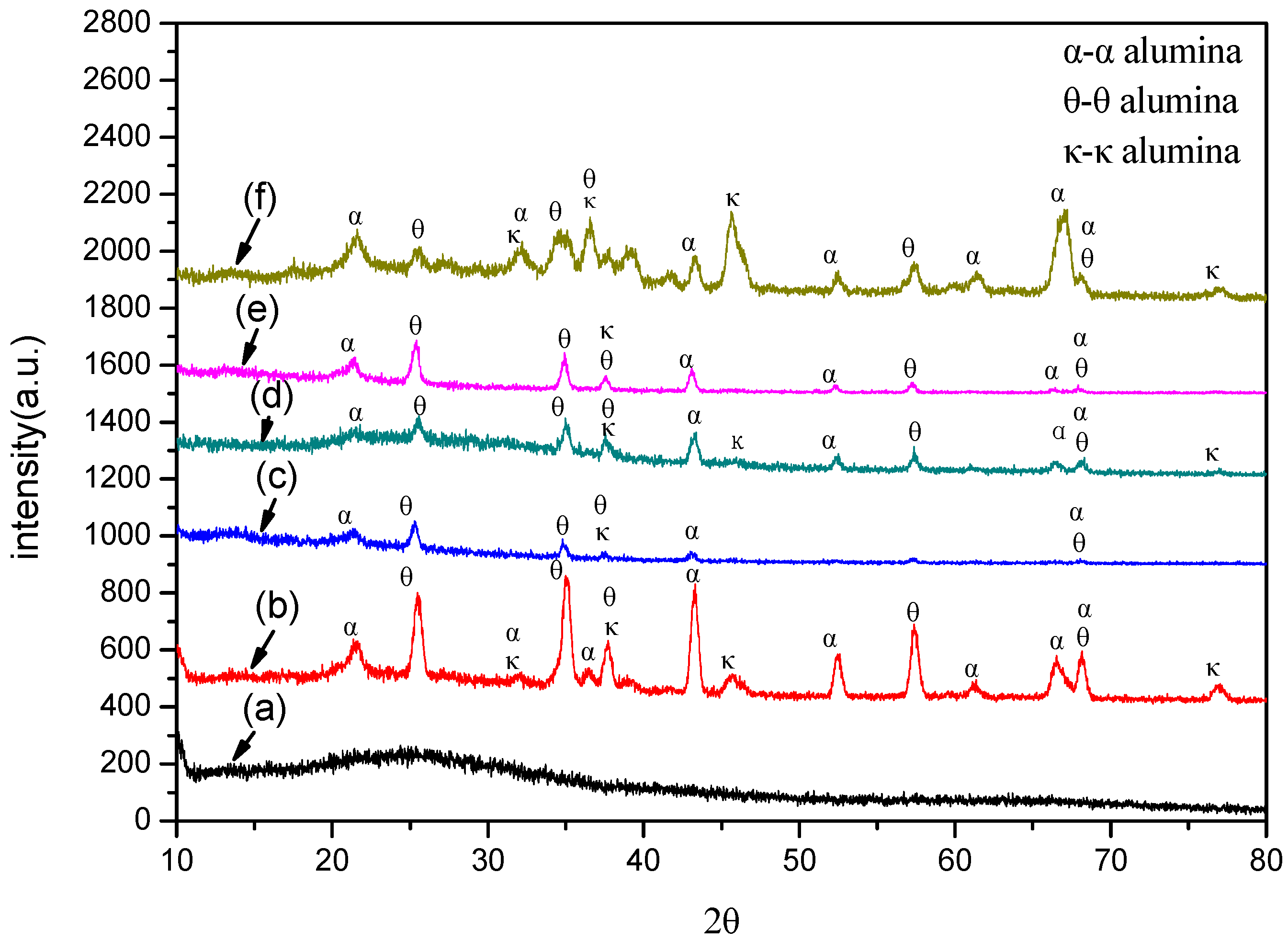
The crystalline phase composition of the pre-anodized coatings after plasma discharges(APD) were analyzed by X-ray diffractometer, the results were compared with anodic and MAO coatings as indicated in Figure 4.
It can be seen from Figure 4 that the anodic coating is composed of amorphous alumina, while the MAO coating was a mixture of various crystalline alumina. The APD coating showed obvious crystallized peaks proving evidence that the non-crystal anodic coating can be transformed to crystal alumina by plasma discharges. It also can be seen from Figure 4 that there were α, θ and κ characteristic peaks in APD coatings and MAO coating crystalline, proved the amorphous alumina could be transformed into crystal alumina. The crystal composition of the APD coating was similar to the MAO coating. The XRD patterns give evidence to the relationship that with the increase of discharge time, current density and duty cycle, the characteristic peak intensity is heightened, thus proving the crystallization transformation increased with the increase of plasma discharge intensity.

3.3. Micro Morphology of the Coatings

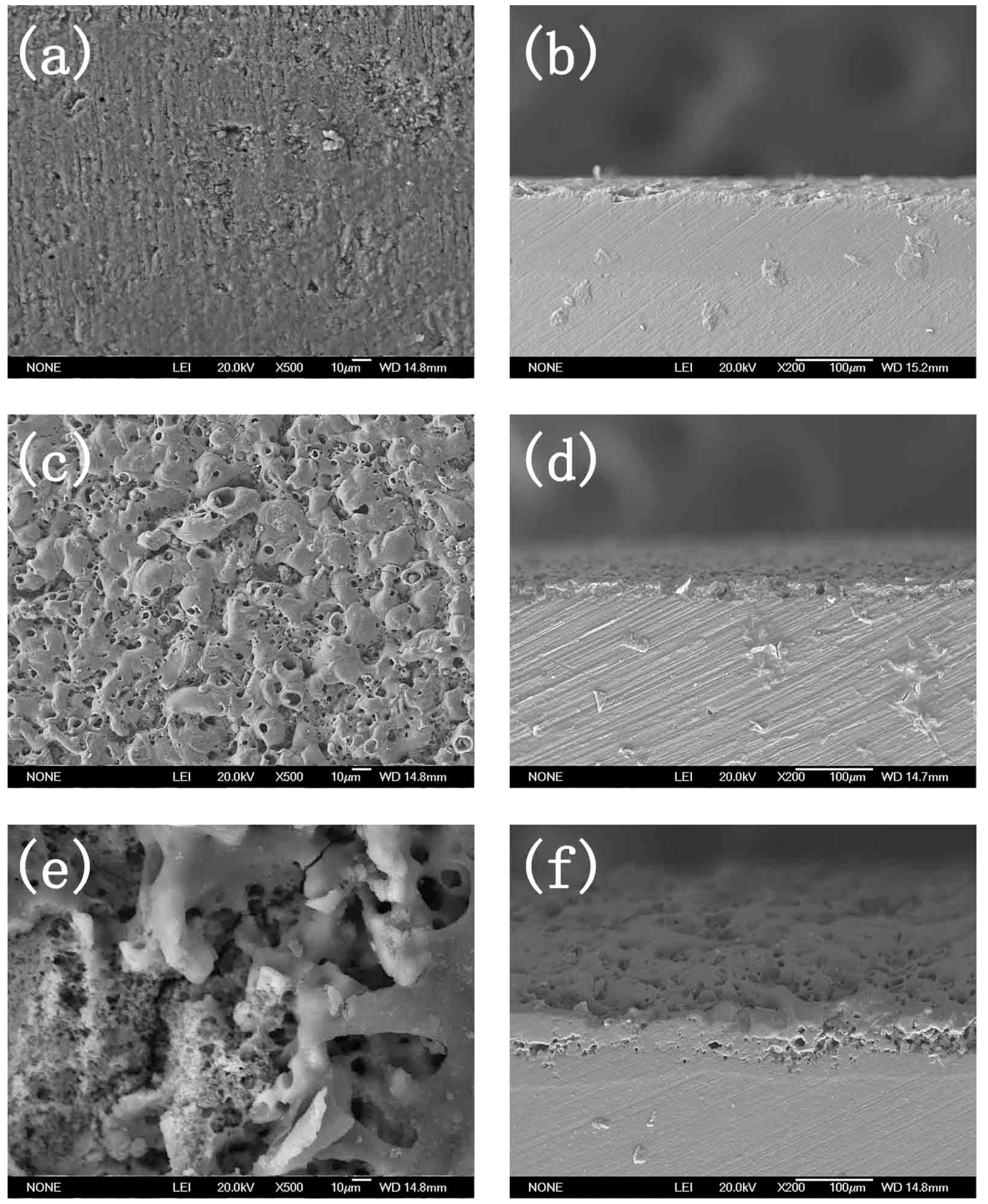
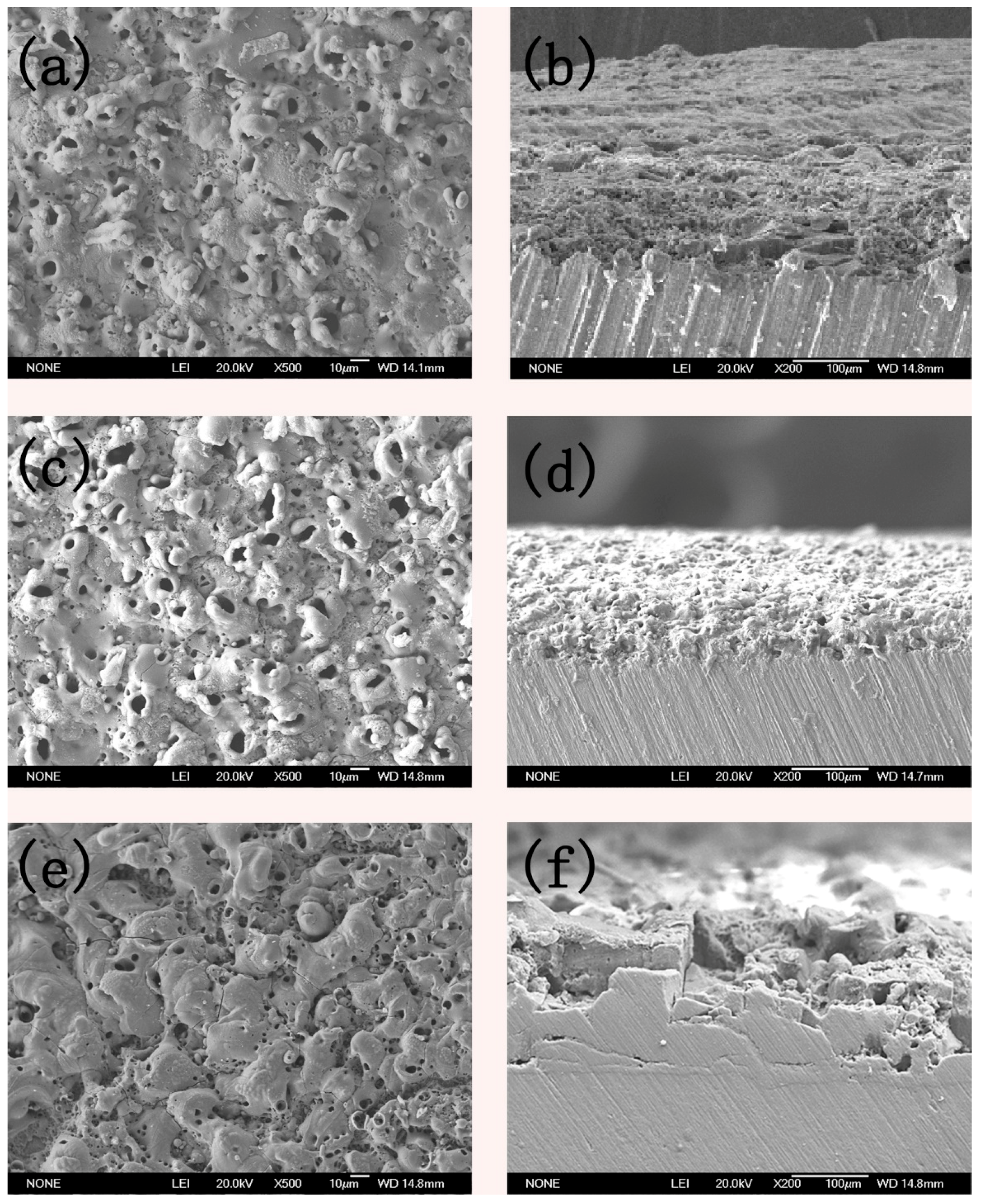
Figure 5 illustrates the micro morphology and cross section of anodizing and MAO coatings with the thickness of 25 microns and 50 microns. It can be seen from Figure 5a,b that the anodic coating has a compact structure, and the MAO coatings generate the typical crater-like features. However, the coating become porous when the thickness reached 50 microns, seen in Figure 5e,f, compared with the thickness of 25 μm, seen in Figure 5c,d.
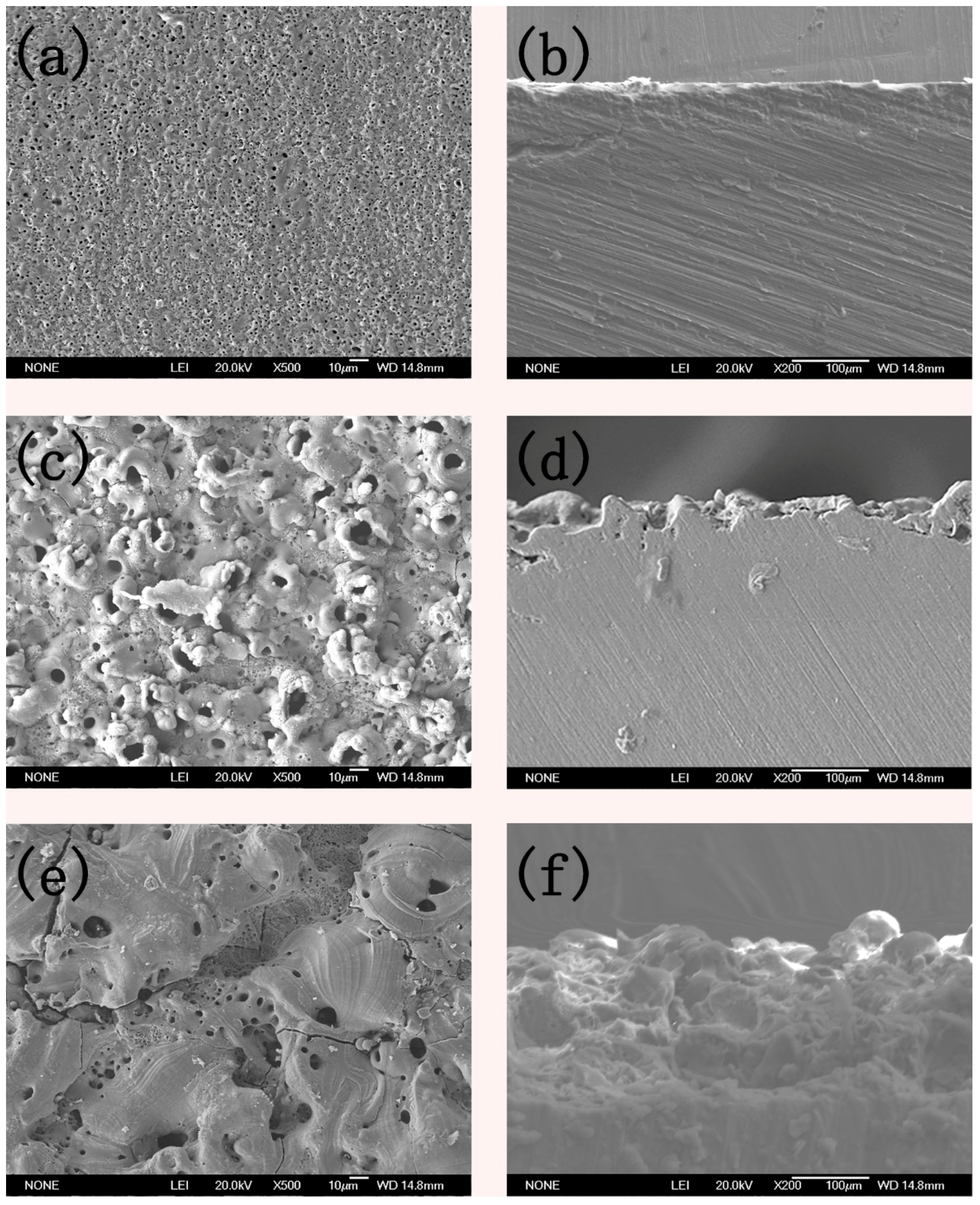
The crystal transformation of pre-anodic coating was related to the heat produced by plasma discharge. The parameters such as current density, duty cycle and discharge time directly effect the heat generated in the discharge process. The influence of current density, duty cycle and discharge time on the micro morphology of the coatings are shown in Figure 6, Figure 7 and Figure 8, respectively.
It can be seen from Figure 6a,c,e that if duty cycle was 15%, and discharge time was 15 min, with the increased of current density from 10 mA/cm2 to 50 mA/cm2, the size of micro pores and cracks increased. It can be seen from Figure 6b,d,f that with growing current density, the crystallization conversion of pre-anodic coating increased.
Figure 7 and Figure 8 illustrate the influence of discharge time and duty cycle on the micro morphology of the coating. There is similar regularity of the influence of current density on the coating. It also can be seen from Figure 6, Figure 7 and Figure 8 that the transformation of amorphous alumina into crystalline alumina was carried out step by step from outside to the substrate. With the increased current density, duty cycle and discharge time, the crystallization conversion and cavitation of the coating increased, however, the number and size of micro cracks in the coating increased.

3.4. Coating Performance

The insulation and thermal conductivity of the coating were tested by a withstand voltage tester and heat conduction coefficient measurement device; results were shown in Table 6.
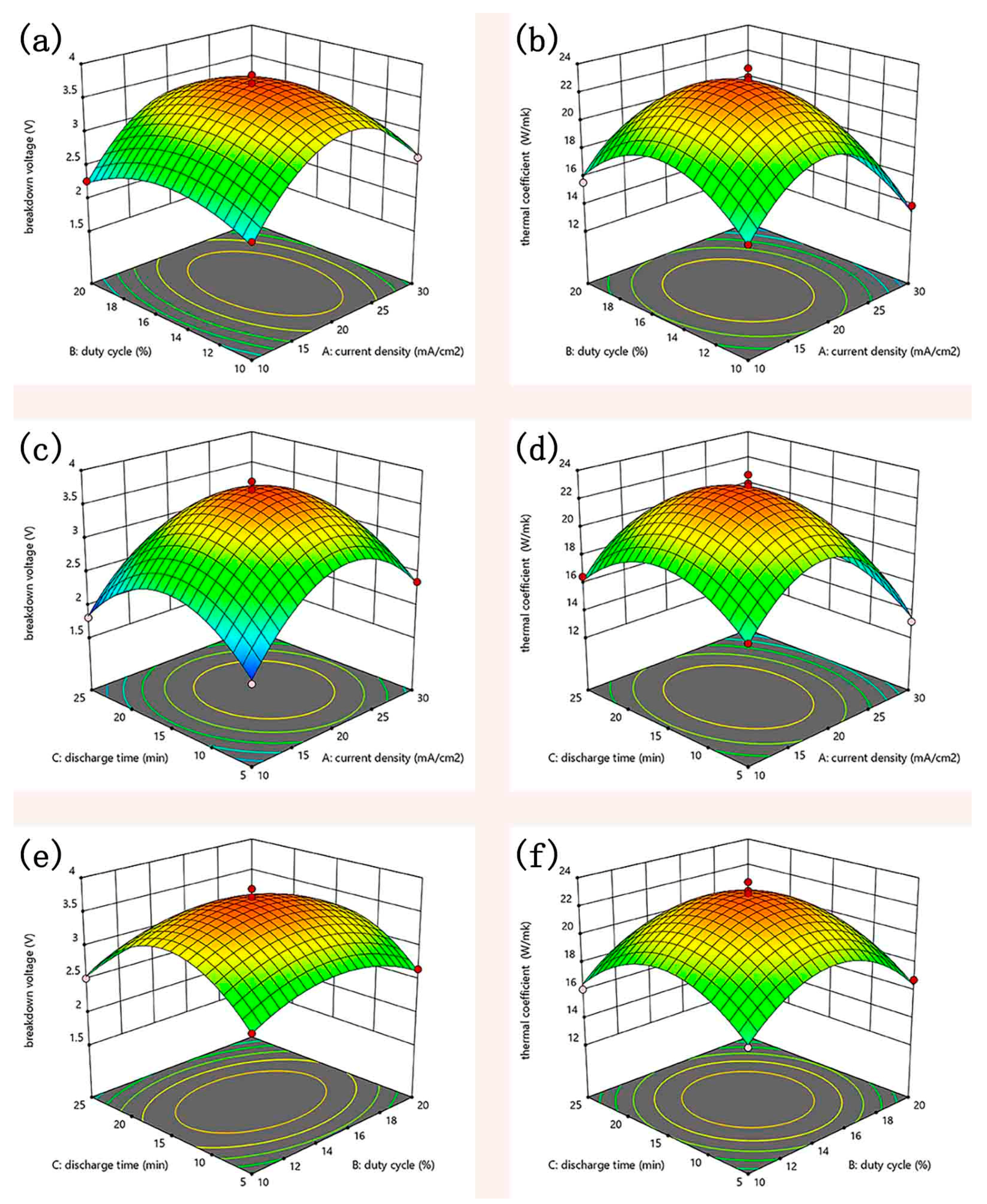
It can be seen from Table 6 that under the condition of current density 20 mA/cm2, duty cycle 15 % and plasma discharge time 15 min, the breakdown voltage and thermal conductivity of the APD coating was 3.81 kV and 23.7 W/m·K, respectively. As plasma discharge was mainly effected by current density, duty cycle and discharge time, and there were strong interactions among these three factors, the interaction of above parameters were analyzed by DESIGN-EXPERT, using Box-Behnken design method, selected breakdown voltage and thermal conductivity as target, with the experiment factors and results shown in Table 7. The interaction of current density, duty cycle and discharge time were analyzed; results are shown in Figure 9.
It can be seen from Figure 9 that there were strong interaction among current density, discharge time and duty cycle, according to the experimental results, the equations of the parameters on the breakdown voltage and thermal conductivity of the coating were obtained and shown as follow:
V = 3.70 + 0.1762 A 0.0325 B 0.0737 C 0.0150 A B 0.0425 A C 0.0350 B C 0.8878 A 2 0.3753 B 2 0.7677 C 2
λ = 17.47 − 1.42A − 0.1000B − 0.0750C − 0.2750AB − 0.0750AC + 0.0250BC
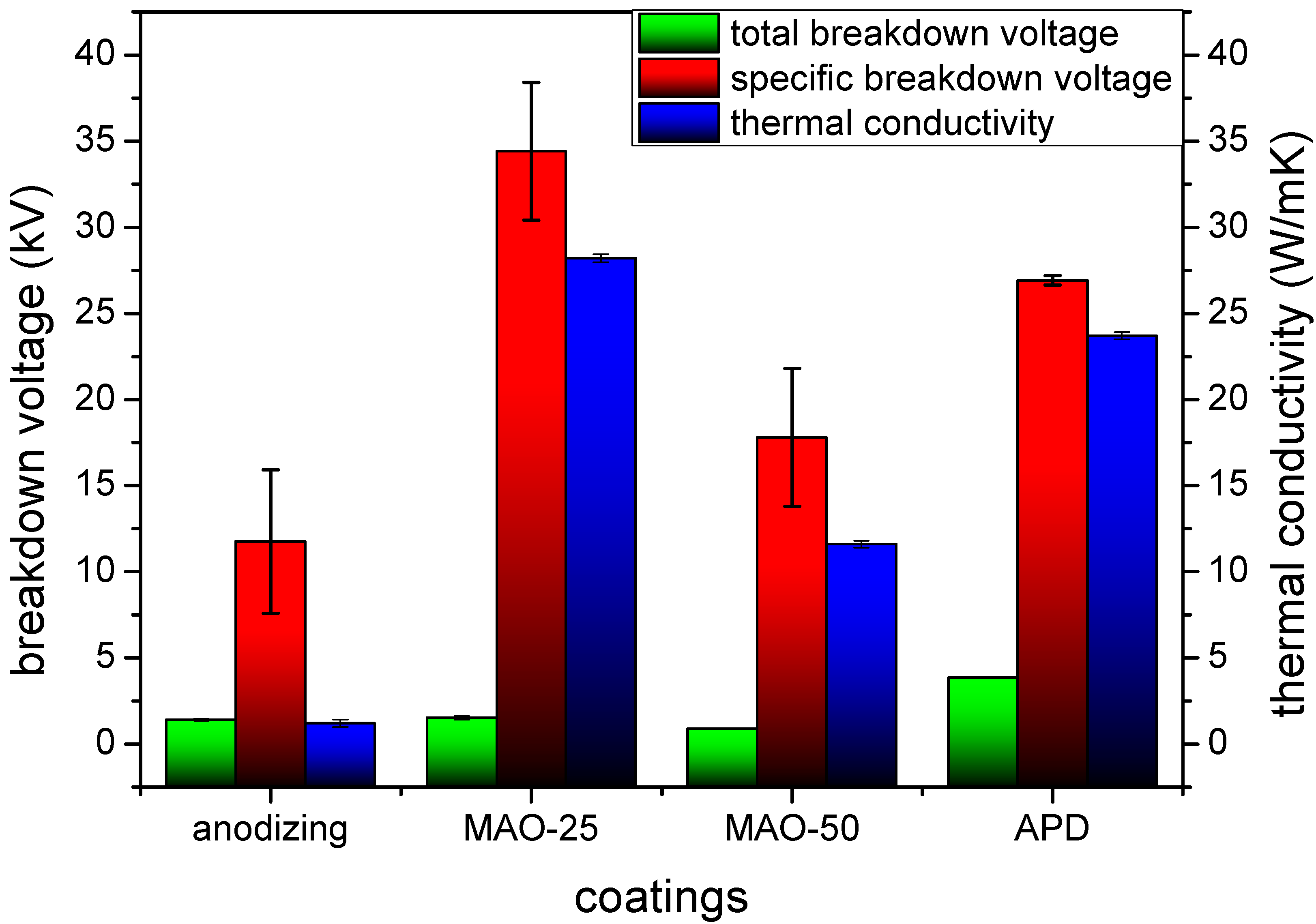
The optimized parameters of plasma discharge were current density of 14 mA/cm2, duty cycle of 15 % and plasma discharge time of 14.5 min. The total and specific breakdown voltage, thermal conductivity of APD at the optimized conditions were tested and compared with anodizing and MAO coating; results are shown in Figure 10.
It can be seen from Figure 10 that the MAO coating with the thickness of 25 μm had the highest specific breakdown voltage (34.4 kV/mm) and thermal conductivity (28.2 W/m·K), yet the total breakdown voltage was close to anodic coating (1.52 kV). When the MAO coating thickness was 50 μm, the specific breakdown voltage (17.8 kV/mm) and thermal conductivity (11.6 W/m·K) decreased significantly. When the pre-anodic coating were treated by plasma discharge, the specific breakdown voltage (26.92 kV/mm) and thermal conductivity (23.7 W/m·K) were close to MAO coating with the thickness of 25 μm, and the total breakdown voltage was 3.85 kV, much higher than anodic or MAO coating.

4. Conclusions

  • A crystalline alumina coating with the thickness of 143 μm was prepared on the pre-anodizing aluminium alloy substrate by the plasma discharge method.
  • The crystalline phase composition of the coating had been characterized by XRD. Results proved the amorphous alumina could be transformed into crystalline alumina, the micro-morphology and cross section of the coatings at different plasma discharge conditions had been observed, and results proved the micro pores and micro cracks increased with the plasma discharge intensity.
  • The total breakdown voltage and thermal conductivity of APD coating was 3.85 kV and 23.7 W/m·K, much higher than that of anodic and MAO coating. The coating can be applied in the heat dissipation of aluminum alloy, meeting the requirement of the high power and small volume part in the electronic industry, especially in LED development.

Author Contributions

Conceptualization, W.S., B.J. and D.J.; methodology, W.S. and B.J.; writing-original draft preparation, W.S.; writing-review and editing, D.J. All authors have read and agreed to the published version of the manuscript.

Funding

This work was supported by the National Natural Science Foundation of China (Grant No. 51571114).

Acknowledgments

The authors would like to thank Y.Z. Du at the University of Xi’an University of Technology for the helpful discussion.

Conflicts of Interest

The authors declare no conflict of interest.

References

  1. Tsai, W.Y.; Huang, G.R.; Wang, K.K.; Chen, C.F.; Huang, J.C. High thermal dissipation of al heat sink when inserting ceramic powders by ultrasonic mechanical coating and armoring. Materials 2017, 10, 454. [Google Scholar] [CrossRef]
  2. Lu, L.; Zhang, Z.; Guan, Y.C.; Zheng, H.Y. Enhancement of heat dissipation by laser micro structuring for led module. Polymers 2018, 10, 886. [Google Scholar] [CrossRef] [PubMed] [Green Version]
  3. Zou, Y.C.; Wang, Y.M.; Xu, S.M. Superhydrophobic double-layer coating for efficient heat dissipation and corrosion protection. Chem. Eng. J. 2019, 362, 638–649. [Google Scholar] [CrossRef]
  4. Lee, J.; Kim, J.; Kim, D.; Chung, W. Heat dissipation performance of metal-core printed circuit board prepared by anodic oxidation and electroless deposition. Thermochim. ACTA 2014, 589, 278–283. [Google Scholar] [CrossRef]
  5. Heo, Y.J.; Kim, H.T.; Kim, K.J.; Nahm, S.; Yoon, Y.J.; Kim, J. Enhanced heat transfer by room temperature deposition of AlN film on aluminum for a light emitting diode package. Appl. Therm. Eng. 2013, 50, 799–804. [Google Scholar] [CrossRef]
  6. Juntunen, E.; Sitomaniemi, A.; Tapaninen, O.; Persons, R.; Challingsworth, M.; Heikkinen, V. Thermal performance comparison of thick-film insulated aluminum substrates with metal core pcbs for high-power led modules. IEEE. Trans. Compon. Packag. Manuf. Technol. 2012, 2, 1957–1964. [Google Scholar] [CrossRef]
  7. Zhu, W.L.; Wang, C.Z.; Sun, M.C.; Li, S.M.; Zhai, J.W.; Lai, T.S. Effect of periodic number of [Si/Sb80Te20]x multilayer film on its laser-induced crystallization studied by coherent phonon spectroscopy. Nanoscale Res. Lett. 2012, 7, 638. [Google Scholar] [CrossRef] [PubMed] [Green Version]
  8. Wu, J.Y.; Chen, C.M.; Horng, R.H.; Wuu, D.S. An efficient metal-core printed circuit board with a copper-filled through (blind) hole for light-emitting diodes. IEEE. Electron Device Lett. 2012, 34, 105–107. [Google Scholar] [CrossRef]
  9. Liang, C.; Kumari, N.; Hou, Y. Thermal resistances of crystalline and amorphous few-layer oxide thin films. AIP Adv. 2017, 7, 115205. [Google Scholar]
  10. Fricke, S.; Friedberger, A.; Schmid, U. The influence of plasma power on the temperature dependant conductivity and on the wet chemical etch rate of sputter-deposited alumina thin films. Surf. Coat. Technol. 2009, 203, 2830–2834. [Google Scholar] [CrossRef]
  11. Liu, H.G.; Xu, Y.D.; Tang, C.L.; Li, Y.; Chopra, N. SiO2 aerogel-embedded carbon foam composite with Co-Enhanced thermal insulation and mechanical properties. Ceram. Int. 2019, 45, 23393–23398. [Google Scholar] [CrossRef]
  12. Kume, S.; Yasuoka, M.; Lee, S.K.; Kan, A.; Ogawa, H.; Watari, K. Dielectric and thermal properties of AlN ceramics. J. Eur. Ceram. Soc. 2007, 27, 2967–2971. [Google Scholar] [CrossRef]
  13. Liu, S.; Liu, J.C.; Du, H.Y.; Hou, F. Hierarchical structural silica-fiber-woven/ mullitewhisker material prepared by surface etching and gas-phase reaction. RSC Adv. 2014, 4, 24307–24310. [Google Scholar] [CrossRef]
  14. Jin, L.; Li, P.Z.; Zhou, H.B.; Zhang, W.; Zhou, G.D.; Wang, C. Improving thermal insulation of TC4 using YSZ-based coating and SiO2 aerogel. Prog. Nat. Sci. 2015, 25, 141–146. [Google Scholar] [CrossRef] [Green Version]
  15. Wen, X.M.; Xiao, Z.Z.; Jiang, T.; Li, J.; Zhang, W.; Zhang, L.; Shao, H.Q. Constructing novel fiber reinforced plastic (frp) composites through a biomimetic approach: Connecting glass fiber with nanosized boron nitride by polydopamine coating. J. Nanomater. 2013, 2013, 155. [Google Scholar] [CrossRef]
  16. Sayyar, M.; Weerasiri, R.R.; Soroushian, P.; Lu, J. Experimental and numerical study of shape-stable phase-changenanocomposite toward energy-efficient building constructions. Energy Build. 2014, 75, 249–255. [Google Scholar] [CrossRef]
  17. Lee, J.; Kim, Y.; Jung, U.; Chung, W. Thermal conductivity of anodized aluminum oxide layer:The effect of electrolyte and temperature. Mater. Chem. Phys. 2013, 141, 680–685. [Google Scholar] [CrossRef]
  18. Mao, F.; Yan, G.Y.; Xuan, Z.J.; Cao, Z.Q.; Wang, T.M. Effect of Eu addition on the microstructures and mechanical properties of A356 aluminum alloys. J. Alloy. Compd. 2015, 650, 896–906. [Google Scholar] [CrossRef]
  19. Sellarajan, B.; Sharma, M.; Ghost, S.K.; Nagaraja, H.S.; Barshilia, H.C. Effect of electrolyte temperature on the formation of highly ordered nanoporous alumina template. Microporous Mesoporous Mater. 2016, 224, 262–270. [Google Scholar] [CrossRef]
  20. Ateş, S.; Baran, E.; Yazıcı, B. The nanoporous anodic alumina oxide formed by two-step anodization. Thin Solid Films 2018, 648, 94–102. [Google Scholar] [CrossRef]
  21. Rogov, A.B.; Slonova, A.I.; Mironov, I.V. The influence of homogeneous electrolyte composition onmicroplasma synthesis and characteristics of Fe-containing coatingson A1050 alloy. Appl. Surf. Sci. 2013, 287, 22–29. [Google Scholar] [CrossRef]
  22. Deng, J.X.; Yun, D.L.; Tan, Y.Q. Design, fabrication and performance of Al2O3/(W0.7Ti0.3)C + Al2O3/TiC multilayered ceramic nozzles. Int. J. Refractory Met. Hard Mater. 2009, 27, 734–739. [Google Scholar]
  23. Rogov, A.B.; Shayapov, V.R. Correlations between the optical emission spectra and microstructure of microplasma coatings on aluminum 2024 alloy. Appl. Surf. Sci. 2012, 258, 4871–4876. [Google Scholar] [CrossRef]
  24. Cheng, F.; Jiang, S.Y.; Liang, J. Cavitation erosion resistance of microarc oxidation coating on aluminium alloy. Appl. Surf. Sci. 2013, 280, 287–296. [Google Scholar] [CrossRef]
  25. Bononi, M.; Giovanardi, R.; Bozza, A.; Mattioli, P. Pulsed current effect on hard anodizing process of 2024-T3 aluminium alloy. Surf. Coat. Technol. 2016, 289, 110–117. [Google Scholar] [CrossRef]
  26. Pradhan, N.R.; Duan, H.; Liang, J.; Iannacchione, G.S. Specific heat and thermal conductivity measurements for anisotropic and random macroscopic composites of cobalt nanowires. Nanotechnology 2008, 19, 485712. [Google Scholar] [CrossRef]
  27. Nampi, P.P.; Ghosh, S.; Warrier, K.G. Calcination and associated structural modifications in boehmite and their influence on high temperature densification of alumina. Ceram. Int. 2011, 37, 3329–3334. [Google Scholar] [CrossRef]
  28. Bosta, M.M.S.A.; Ma, K.J. Influence of electrolyte temperature on properties and infrared emissivity of MAO ceramic coating on 6061 aluminum alloy. Infrared Phys. Technol. 2014, 67, 63–72. [Google Scholar] [CrossRef]
  29. Dehghannya, J.; Farshad, P.; Heshmati, M.K. Three-stage hybrid osmotic-intermittent microwave-convective drying of apple at low temperature and short time. Dry. Technol. 2018, 36, 1982–2005. [Google Scholar] [CrossRef]
  30. Arieli, R.; Marmur, A. Decompression sickness bubbles: Are gas micronuclei formed on a flat hydrophobic surface. Respir. Physiol. Neurobiol. 2011, 177, 19–23. [Google Scholar] [CrossRef]
  31. Patermarakis, G. Thorough electrochemical kinetic and energy balance models clarifying the mechanisms of normal and abnormal growth of porous anodic alumina films. J. Electroanal. Chem. 2014, 730, 69–85. [Google Scholar] [CrossRef]
  32. Saffari, H.; Sohrabi, B.; Noori, M.R.; Bahrami, H.R.T. Optimal condition for fabricating superhydrophobic Aluminum surfaces with controlled anodizing processes. Appl. Surf. Sci. 2018, 435, 1322–1328. [Google Scholar] [CrossRef]
  33. Chung, I.C.; Chung, C.K.; Su, Y.K. Effect of current density and concentration on microstructure and corrosion behavior of 6061 Al alloy in sulfuric acid. Surf. Coat. Technol. 2017, 313, 299–306. [Google Scholar] [CrossRef]
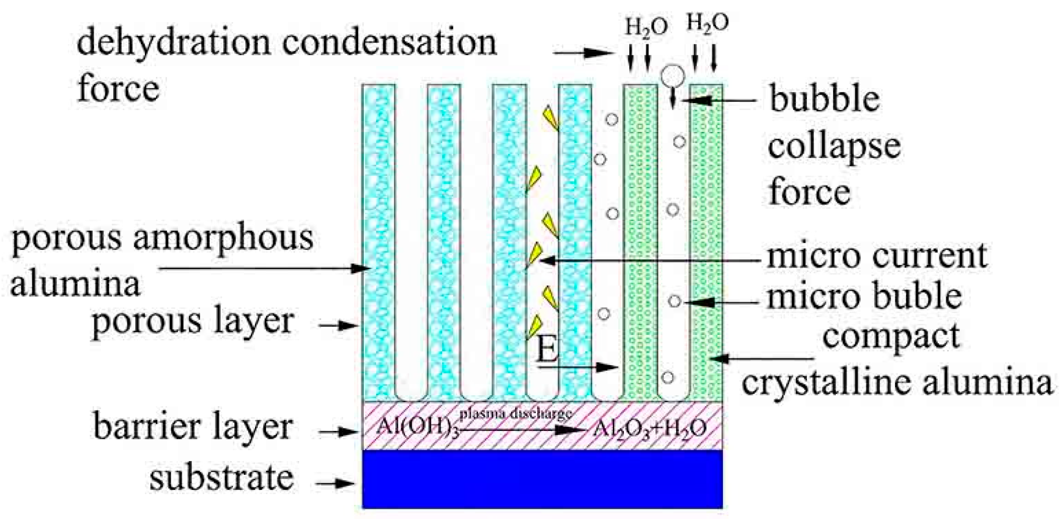
Figure 1. Crystalline phase transformation mechanism of pre-anodic coating.
Coatings 10 00038 g001
Figure 2. The direction of (a) single and (b) multiple bubble collapse force.
Coatings 10 00038 g002
Figure 3. Influence of sulfuric and phosphoric acid concentration on the (a) thickness and (b) uniformity of AAO coating.
Coatings 10 00038 g003
Figure 4. XRD patterns of (a) anodic, (b) MAO and APD coatings at (c) discharge time 5 min, duty cycle 10% and current density 100 mA/cm2 (d) discharge time 15 min, duty cycle 15% and current density 100 mA/cm2 (e) discharge time 15 min, duty cycle 10% and current density 200 mA/cm2 (f) discharge time 25 min, duty cycle 20% and current density 500 mA/cm2.
Coatings 10 00038 g004
Figure 5. Micro-morphology (a,c,e) and cross section (b,d,f) of anodic (a,b) and MAO coating with thickness of 25 microns (c,d) and 50 micons (e,f).
Coatings 10 00038 g005
Figure 6. Micro-morphology (a,c,e) and cross section (b,d,f) of APD coating at current density of 10 mA (a,b), 20 mA (c,d) and 50 mA (e,f).
Coatings 10 00038 g006
Figure 7. Micro-morphology (a,c,e) and cross section (b,d,f) of APD coating at discharge time of 5 min (a,b), 15 min (c,d) and 25 min (e,f).
Coatings 10 00038 g007
Figure 8. Micro-morphology (a,c,e) and cross section (b,d,f) of APD coating at duty cycle of 10 % (a,b), 15 % (c,d) and 20 % (e,f).
Coatings 10 00038 g008
Figure 9. The interaction effect of current density, duty cycle and discharge time on the breakdown voltage (a,c,e) and thermal conductivity (b,d,f) of the APD coating.
Coatings 10 00038 g009
Figure 10. The breakdown voltage and thermal conductivity of anodizing, MAO and APD coatings.
Coatings 10 00038 g010
Table 1. Insulation and thermal conductivity of different materials.
MaterialsDielectric Strength (kV/mm)Thermal Conductivity (W/m·K)
amorphous alumina [9]200.205
α-alumina [10]20–4026–50
Silica [11]3.81.4
aluminum nitride [12]870–210
insulation gasket [13]31.0–5.0
insulation grease [14]2.75–4.21.0–5.0
insulation adhesive [15]30.5–2.0
graphite sheets [16]-end-wise 3.0–5.0
Air [9]10.025
Table 2. Micro-structure parameters of aluminum alloy anodic coatings in different electrolyte.
Kind of AcidAperture/nmCoating Thickness
/μm
Hole Wall Thickness
/nm
Pore Volume
/ %
Number of Holes
Quantity × 109/cm2
sulfuric acid [28]12200–4000.807.576
phosphate acid [29]3350–601.1419
chromic acid [30]242–51.09422
oxalic acid [31]17200.97235
Table 3. The composition of aluminum 6061 alloy.
CompositionAlMgSiCuCrFeMnZnTi
wt %balance0.8–1.20.4–0.80.15–0.40.04–0.350.70.150.250.15
Table 4. Parameters of anodizing process.
Experiment NumberConcentration of H2SO4
(g/L)
Concentration of H3PO4
(g/L)
Experiment NumberConcentration of H2SO4
(g/L)
Concentration of H3PO4
(g/L)
1379.51173.528.5
2191238
328.513929.5
4381419
5559.51528.5
6191638
728.5171859.5
8381819
973.59.51928.5
10192038
Table 5. Parameters of MAO process.
Experiment NumberCurrent Density
(mA/cm2)
Plasma Discharge Time
(min)
Duty Cycle
(%)
110510
220510
350510
420510
5201510
6202510
7201515
8201520
Table 6. The breakdown voltage and thermal conductivity of APD coating at different conditions.
Coating PerformanceCurrent DensityDuty Cycle Discharge Time
mA/cm2%min
10205010152051525
Breakdown voltage (kV)3.242.591.061.842.231.772.123.811.61
Thermal conductivity (W/m·K)20.117.711.312.1521.1416.8218.123.716.2
Table 7. Experimental factors and results of BOX-Behnken design method.
StdRunFactor 1
A:Current Density
(mA/cm2)
Factor 2
B:Duty Cycle (%)
Factor 3
C:Discharge Time
(min)
Response 1
Breakdown Voltage
(kV)
Response 2
Thermal Coefficient
(W/m·K)
51101551.8416.3
1222020252.4116.5
131010152.3315.8
443020152.5112.6
253010152.6313.9
1462015153.6423.7
371020152.2715.6
68301552.3613.2
1192010252.5216.1
7101015251.8116.5
1011202052.6616.8
15122015153.8122.5
13132015153.6123.1
16142015153.7222.9
8153015252.1613.1
17162015153.6821.9
917201052.6316.5