Article

Systematic Study of the SiOx Film with Different Stoichiometry by Plasma-Enhanced Atomic Layer Deposition and Its Application in SiOx/SiO2 Super-Lattice

1
State Key Laboratory of ASIC and System, Shanghai Institute of Intelligent Electronics & Systems, School of Microelectronics, Fudan University, Shanghai 200433, China
2
SMIT Center, School of Automation and Mechanical Engineering, Shanghai University, Shanghai 201800, China
3
Shanghai Key Laboratory of Modern Optical System, School of Optical-Electrical and Computer Engineering, University of Shanghai for Science and Technology, Shanghai 200093, China
4
Department of Mechanical Engineering Science, University of Johannesburg, Johannesburg ZA-2006, South Africa
*
Author to whom correspondence should be addressed.
Nanomaterials 2019, 9(1), 55; https://doi.org/10.3390/nano9010055
Submission received: 13 December 2018 / Revised: 26 December 2018 / Accepted: 27 December 2018 / Published: 3 January 2019

Abstract

:
Atomic scale control of the thickness of thin film makes atomic layer deposition highly advantageous in the preparation of high quality super-lattices. However, precisely controlling the film chemical stoichiometry is very challenging. In this study, we deposited SiOx film with different stoichiometry by plasma enhanced atomic layer deposition. After reviewing various deposition parameters like temperature, precursor pulse time, and gas flow, the silicon dioxides of stoichiometric (SiO2) and non-stoichiometric (SiO1.8 and SiO1.6) were successfully fabricated. X-ray photo-electron spectroscopy was first employed to analyze the element content and chemical bonding energy of these films. Then the morphology, structure, composition, and optical characteristics of SiOx film were systematically studied through atomic force microscope, transmission electron microscopy, X-ray reflection, and spectroscopic ellipsometry. The experimental results indicate that both the mass density and refractive index of SiO1.8 and SiO1.6 are less than SiO2 film. The energy band-gap is approved by spectroscopic ellipsometry data and X-ray photo-electron spectroscopy O 1s analysis. The results demonstrate that the energy band-gap decreases as the oxygen concentration decreases in SiOx film. After we obtained the Si-rich silicon oxide film deposition, the SiO1.6/SiO2 super-lattices was fabricated and its photoluminescence (PL) property was characterized by PL spectra. The weak PL intensity gives us greater awareness that more research is needed in order to decrease the x of SiOx film to a larger extent through further optimizing plasma-enhanced atomic layer deposition processes, and hence improve the photoluminescence properties of SiOx/SiO2 super-lattices.

1. Introduction

Compatible with common micro-electronic device fabrication techniques and materials [1,2], silicon (Si) based micro-nano devices have become the most promising material for advanced integrated opto-electronic technologies in the future [3]. Since the discovery of efficient photoluminescence in the red region in porous Si at room temperature [4], silicon nanocrystals (Si-NCs) were extensively studied in the last decade [5,6]. Particularly in recent years, Si-NCs have aroused significant attention in the applications of light sources and “all-silicon” devices like silicon lasers, light emitting diode (LED), flash memories [7,8], and tandem solar cells. Among the different techniques of Si-NCs fabrication in a solid matrix, super-lattices were considered to be very effective in producing size-, density-, and shape-controlled Si-NCs [9,10,11].
A large number of studies have been reported on Si-NCs embedded in silicon dioxide (SiO2) [12,13,14]. Based on the quantum confinement theory [15,16,17], the correlation between the photoluminescence (PL) properties and the size of the nanocrystals has been established. Control over all three parameters (size, density, spherical shape) can be reached by depositing thin alternating layers of stoichiometric and Si rich dielectrics in the form of a superlattice (SL). This approach has been well established for silicon nanocrystals in SiO2 matrix. However, most of the Si-NCs and superlattices in previous studies are fabricated by chemical vapor deposition (CVD) [18,19,20], sputtering [21,22,23], or other deposition techniques [24], these techniques are good at depositing thick film but weak in thin film. Which hamper the further study on the control of Si-NCs in superlattice with ultrathin dielectric film or barrier layer. Atomic layer deposition (ALD) is a promising technology for advanced thin film deposition as it offers excellent control at the atomic scale over the thickness and uniformity of the film [25,26,27]. It allows the precise preparation of size- and distribution-controlled silicon nanocrystals. So, it will be a wonderful opportunity to fabricate silicon oxides and related superlattice by ALD technique, and study its photoluminescence properties.
There have been a certain amount of studies on the growth of SiO2 film using ALD [28,29,30], but rarely on the control of its stoichiometry and optical/electrical properties. Thus, in this study, plasma- enhanced atomic layer deposition (PEALD) was used to deposit SiOx film with different stoichiometry. In detail, ALD deposition parameters were firstly studied to understand the effect of deposition parameters like precursor pulse time and temperature on the growth properties of SiOx film. Upon choosing suitable deposition parameters, three kinds of film (SiO2, SiO1.8, and SiO1.6) with different stoichiometry were acquired successfully. Film properties like physical, chemical, and photo-electrical properties of SiOx film with different stoichiometry were studied systematically. Specifically, basic film characteristics including microstructure, density, and roughness were evaluated, while the chemical bonding character of the obtained film was discussed by Si 2p and O 1s in detail. Furthermore, the energy band-gap of the SiOx film with different stoichiometry was identified by both spectroscopic ellipsometry (SE) data analysis and X-ray photo-electron spectroscopy (XPS) measurements. Finally, to examine the properties of Si rich SiOx obtained by ALD in this study, SiO1.6/SiO2 superlattice was fabricated and its photoluminescence property was characterized by PL spectra.

2. Experimental Section

2.1. Film Preparation

SiOx films were deposited on p-type (1–10 Ω·cm), single polished, Si(100) wafers in a BENEQ TFS200 ALD system (BENEQ, Finland) at a vacuum degree of 1 mbar. Prior to deposition, the Si wafers were cleaned by a standard RCA process followed by a deionized water rinsing and drying in N2. During the deposition process, precursors of Si and O were tris(dimethylamino)silane (TDMAS) and O2 plasma. TDMAS was purchased from Fornano company and maintained at 20 °C in a stainless bottle. The O2 plasma was activated at 200 W. The schematic diagram of one ALD cycle of SiOx growth utilized in this work is illustrated in Figure 1a. Each ALD cycle contains four steps: TDMAS pulse, Ar purge, plasma processing, and Ar purge.

2.2. Sample Characterization

The surface morphology was observed using an atomic force microscope (AFM, Bruker, icon), and a typical 5 μm × 5 μm area was investigated using non-contact mode. Transmission electron microscopy (TEM) (FEI, TECNAI G2 F20) was used to analyze the micro-structure and interface composition of the silicon oxides. The chemical bonding character of the obtained film was characterized by XPS (SPECS, Berlin, Germany) using a mono-chromatic Al Kα source (hν = 1486.6 eV). A narrow scan resolution of 0.1 eV was used. The adventitious C 1s peak, arising from traces of hydrocarbon in the spectrometer, was used as a reference for evaluating the peak positions because of static charging of samples. The C 1s peak position was observed together with other peaks (Si 2p, N 1s, and O 1s) of the spectrum, and all the XPS spectra were calibrated by the C 1s peak at a binding energy of 284.6 eV. The micro-structure and morphology of the film were characterized by X-ray reflection (XRR) (Bruker, D8, Billerica, MA, USA). SE measurements were carried out on a rotating analyzer ellipsometer (SOPRA, GES-5E, Annecy, France). The incident angle was 75°. The spectral wavelength range from 190 to 800 nm, the system measured the spectra of Ψ and Δ as functions of wavelength (λ). The resulting spectra was fitted with WinElli_II software. PL spectroscopy was used to investigate the optical properties of Si-NCs produced within the SiOx/SiO2 super-lattice. The PL was excited by the 325 nm line of HeCd laser. The PL signal was focused into a single monochromator and detected by a nitrogen-cooled charge-coupled device (CCD) camera. All spectra were corrected for the spectral response of the measurement system.

3. Results and Discussion

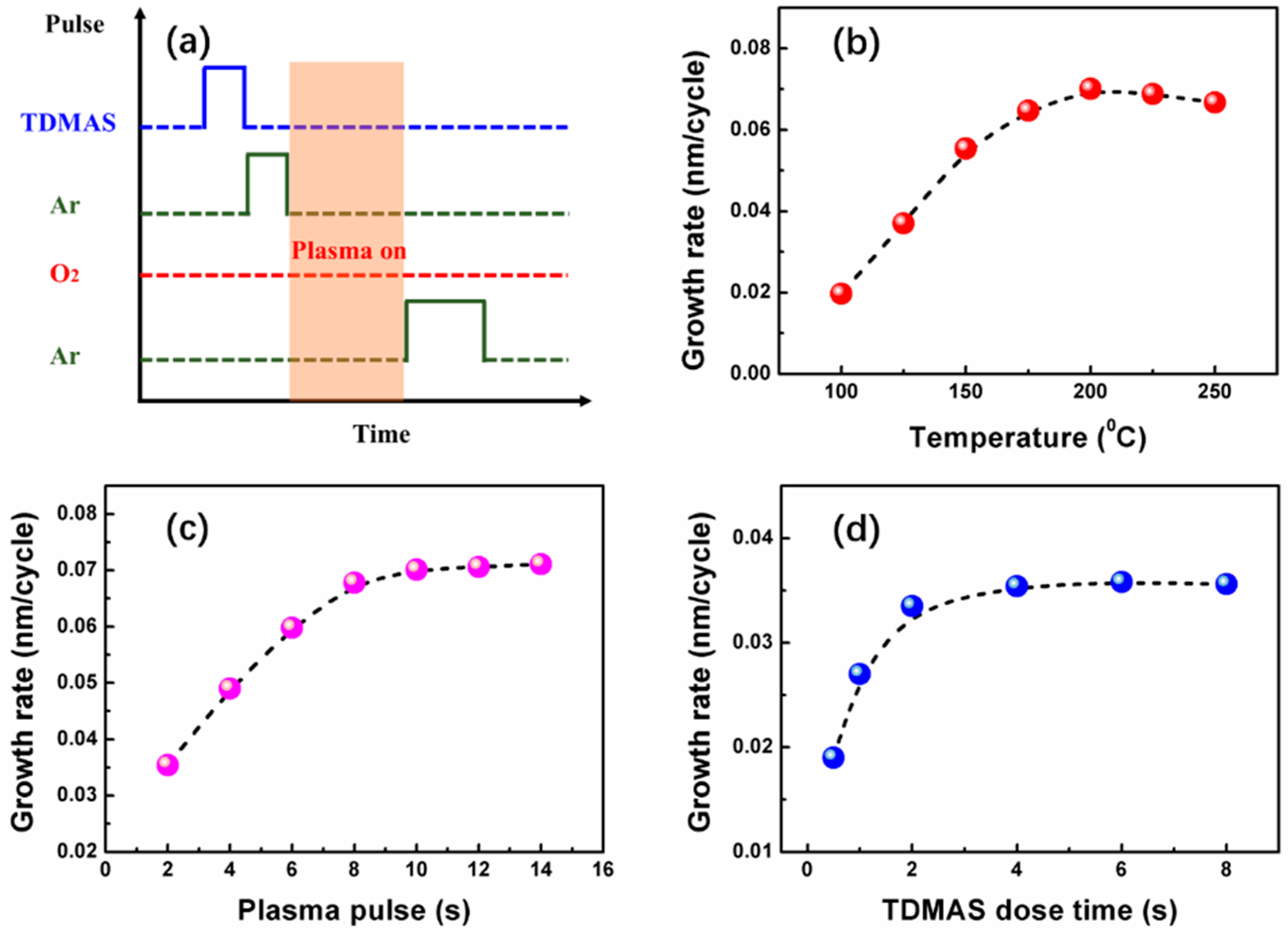
3.1. Film Fabrication and Growth Rate Experiments

In order to optimize the growth parameters needed for the self-limiting deposition of SiOx thin film, the effect of temperature, TDMAS dose, and O2 plasma duration was studied. At first, with the purpose of studying the effect of temperature on growth rate, 100 cycles with 2 s TDMAS and 8 s O2 plasma was deposited at different temperatures (100–250 °C). The growth rate increased initially as the temperature was increased from 100 to 175 °C. However, it stayed nearly constant at an ALD temperature window from 175 °C to 250 °C, as seen in Figure 1b, where deposition rate was constant at 0.07 nm/cycle. Figure 1c,d display the growth rate of the SiOx thin film as a function of plasma time and TDMAS pulse time at a deposition temperature of 200 °C. The O2 flow rate was fixed at 50 sccm. The growth rate was determined here in terms of the film thickness divided by the total number of applied ALD cycles. The film thickness was 7.08, 9.8, 11.96, 13.56, 14.02, 14.13, and 14.21 nm for the samples with the plasma pulse time of 2, 4, 6, 8, 10, 12, and 14 s, respectively. The total ALD cycles were kept at 200 for the simulation. It can be observed from Figure 1c that the growth rate increases initially as plasma time increases. It remained constant at 0.071 nm/cycle when the plasma time was greater than 8 s. To obtain the saturated TDMAS pulse time, the plasma pulse time was kept at 8 s. The film thickness became 3.8, 5.4, 6.7, 7.08, 7.16, and 7.12 nm when the TDMAS pulse time was set as 0.5, 1, 2, 4, 6, and 8 s, respectively. As seen in Figure 1d, deposition rate was saturated for TDMAS pulse time starting from 2 s. These results suggest that the SiOx thin film was grown in a self-limiting manner when using the PEALD technique.
Figure 2 shows the 5 μm2 × 5 μm2 AFM images for SiO2 thin films with different deposition temperatures. It is clear that the morphology changes with different temperatures. As the deposition temperature increases, the resulting morphology transforms from an island structure into a slim needle like structure. The surface root mean-square (RMS) roughness becomes lower with the increase in deposition temperature. For SiO2 thin film deposited at 100 °C, it presents the maximum roughness of 0.52 nm, then the value decreases to 0.43, 0.27, and 0.26 nm for the films deposited at 150, 200, and 250 °C, respectively. It was found that the surface roughness of all the films prepared in this work is very small, indicating that the films have a smooth surface.
Then, the three sample sets (S1, S2, and S3) were prepared in order to obtain SiOx film with different stoichiometry. In ALD deposition, the temperature was fixed at 250 °C. The precursor pulse time was changed in order to obtain silicon oxides of stoichiometric (SiO2) and non-stoichiometric (SiOx, x < 2). To be specific, TDMAS pulse time was 2, 2, and 4 s for S1, S2, and S3 sample, respectively, O2 plasma duration was 8, 4, and 2 s for S1, S2, and S3 film, respectively. The purge time was always kept at 4 s no matter whether it was after the TDMAS pulse or after the O2 plasma. Meanwhile, in order to decrease the oxygen content in the film to form Si rich silicon dioxide, the O2 flow rate was also adjusted, it was 50 sccm, 50 sccm, and 25 sccm on the deposition of S1, S2, and S3 film, respectively.
After deposition, all samples were tested by XPS to determine the stoichiometric. Figure 3 displays the XPS wide scan spectrum of S1, S2, and S3 film after Ar+ ion treatment. The determined XPS peaks of Si, O, and C are stated in the figure. All the peaks of elements are marked and recognized in detail. By comparing the content of Si and O element in three samples, it is found that the stoichiometries are x = 2, 1.8, and 1.6 for S1, S2, and S3 film, respectively. Which means that the S1 sample is the silicon dioxide film of stoichiometric and S2 and S3 samples are silicon dioxide of nonstoichiometric.

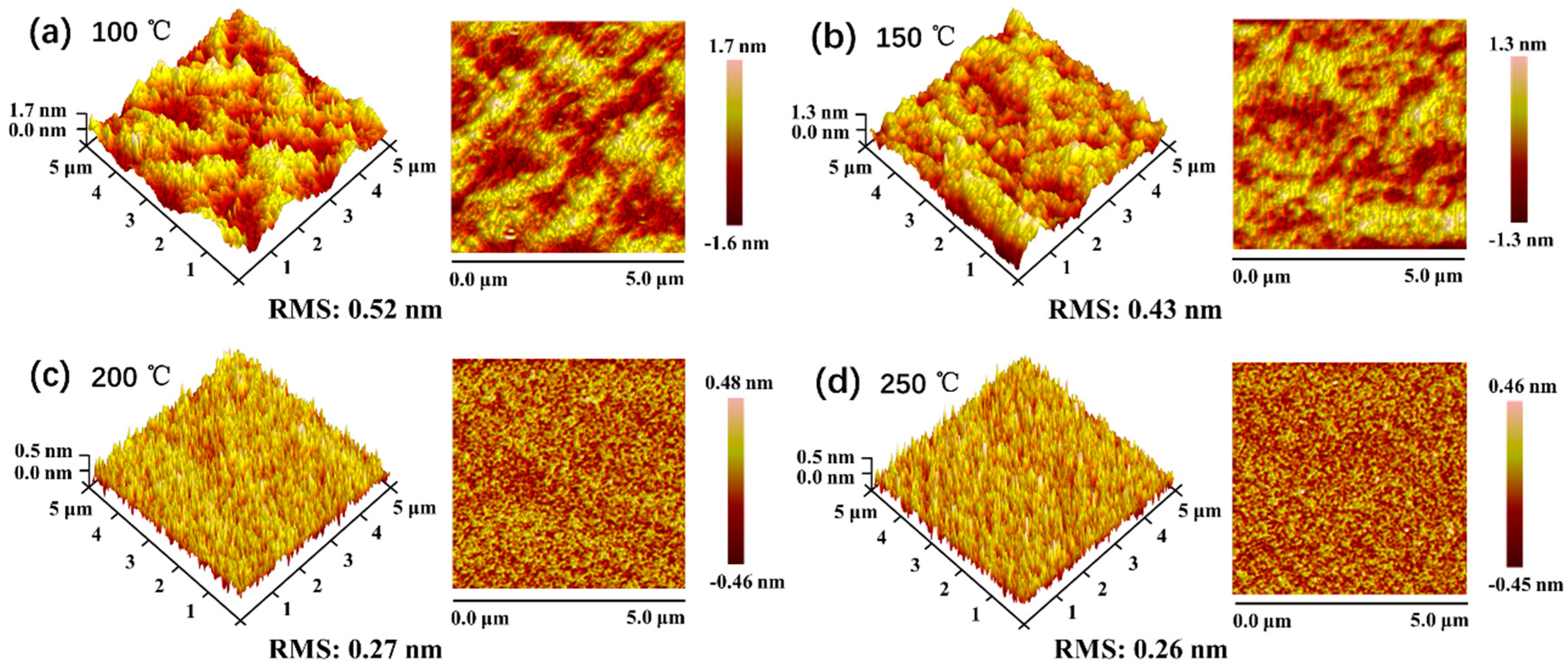
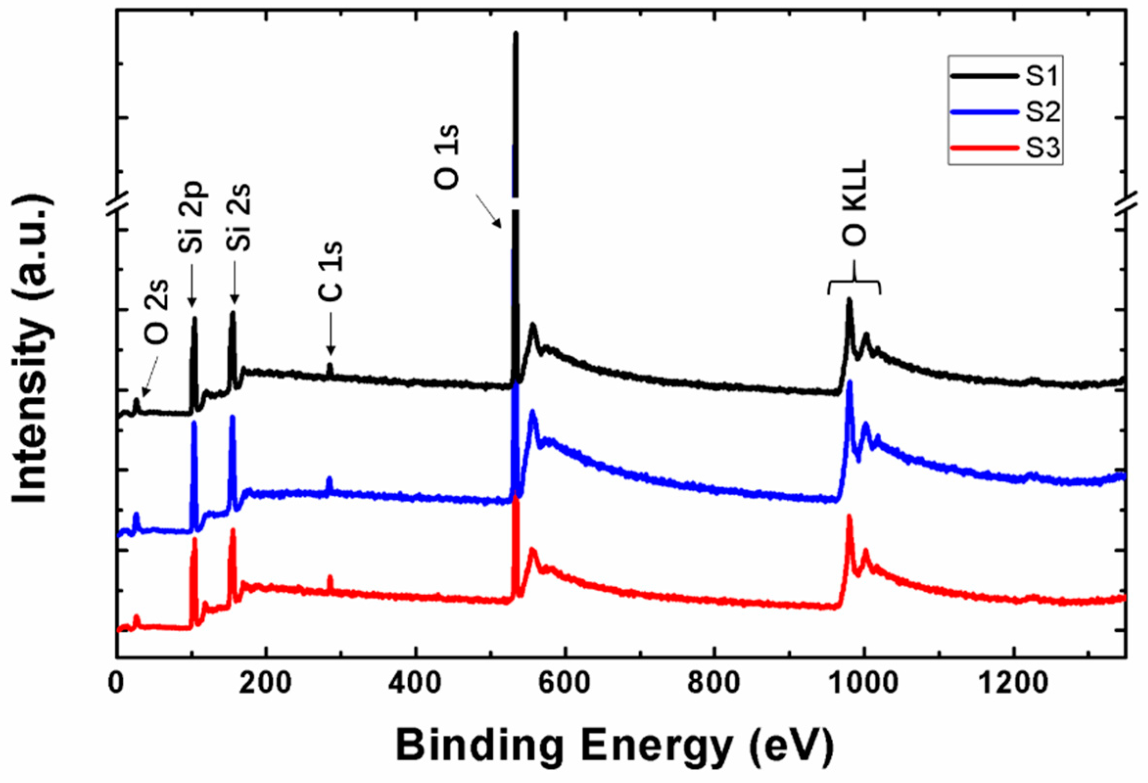
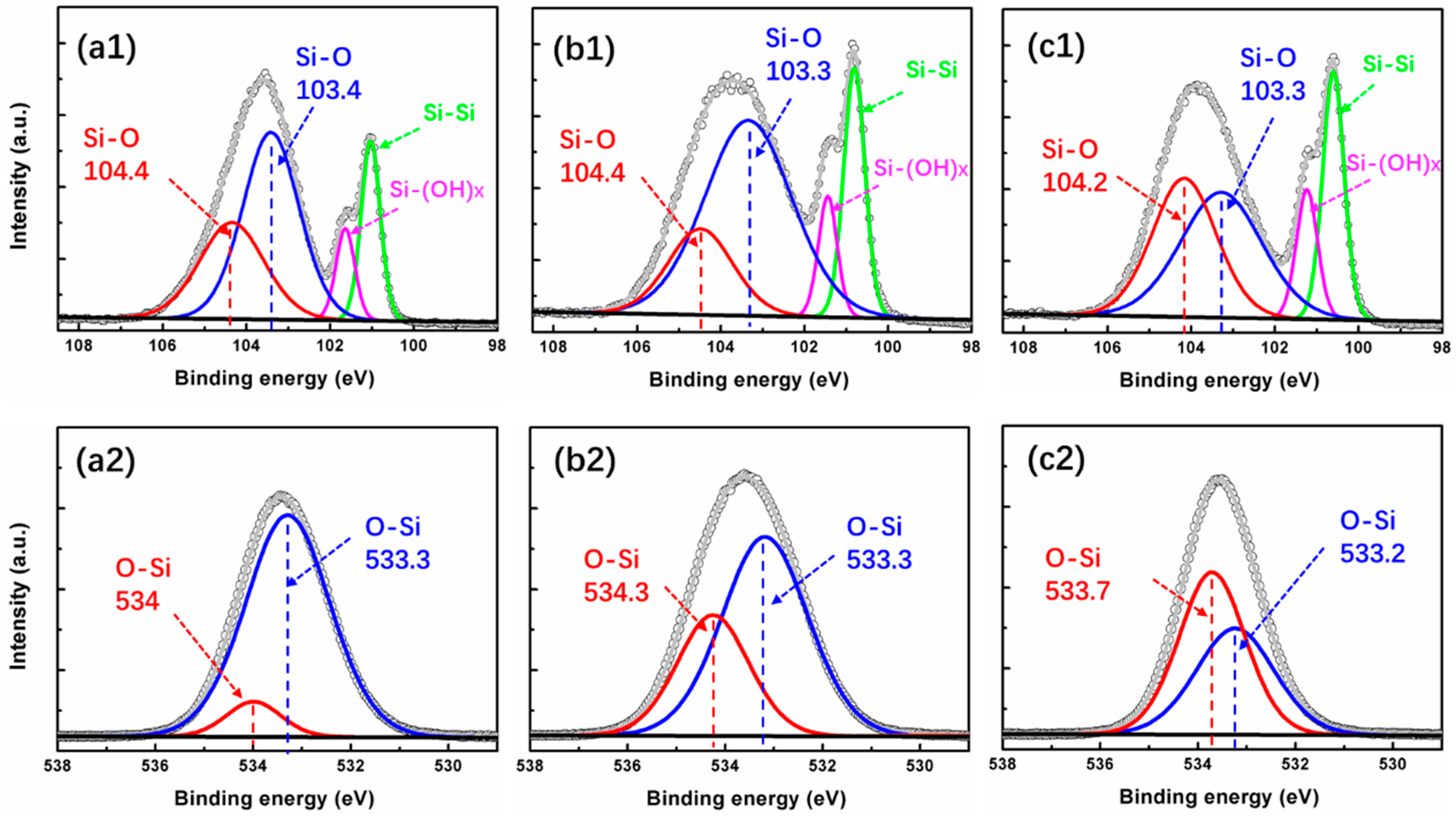
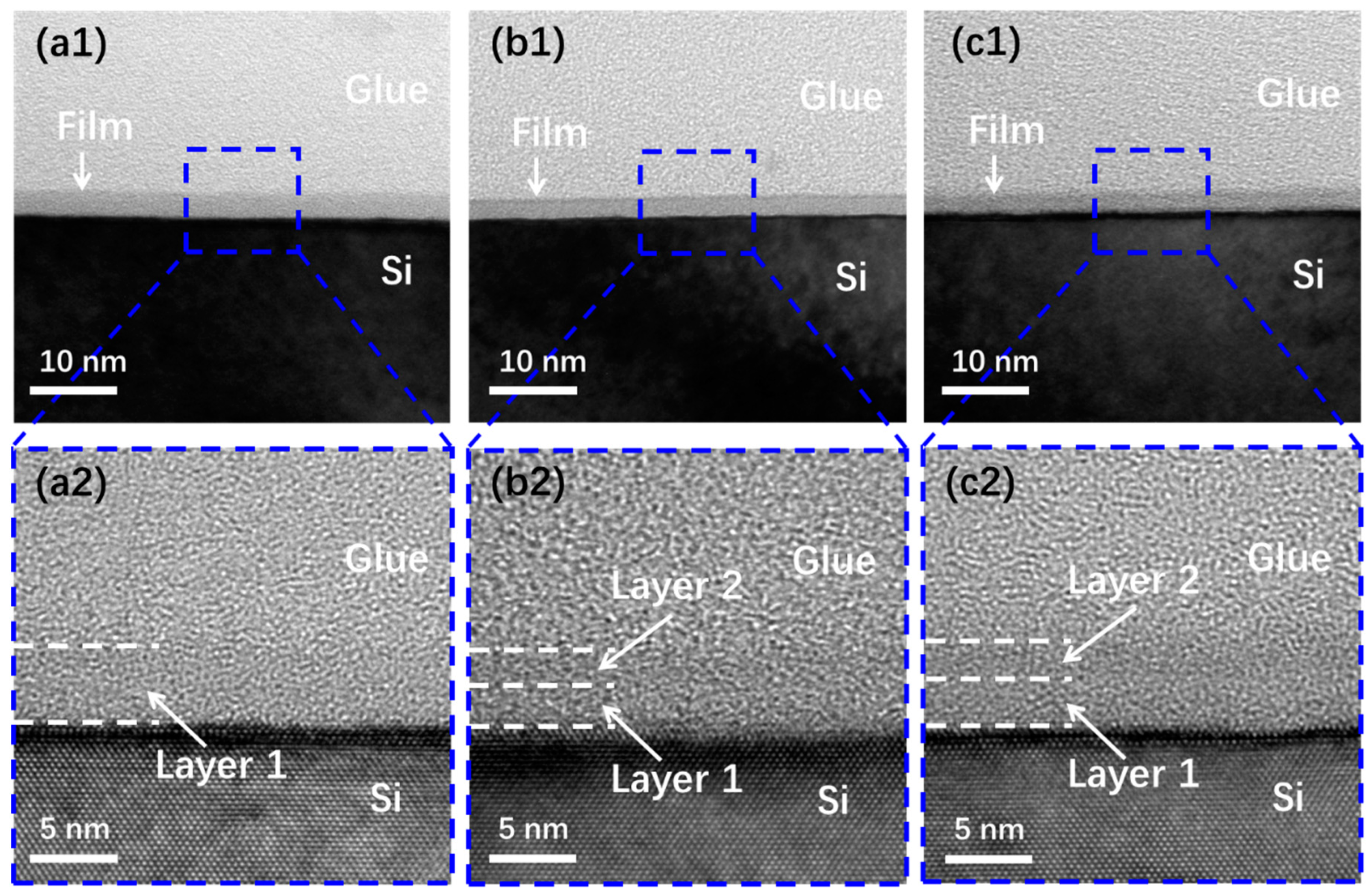
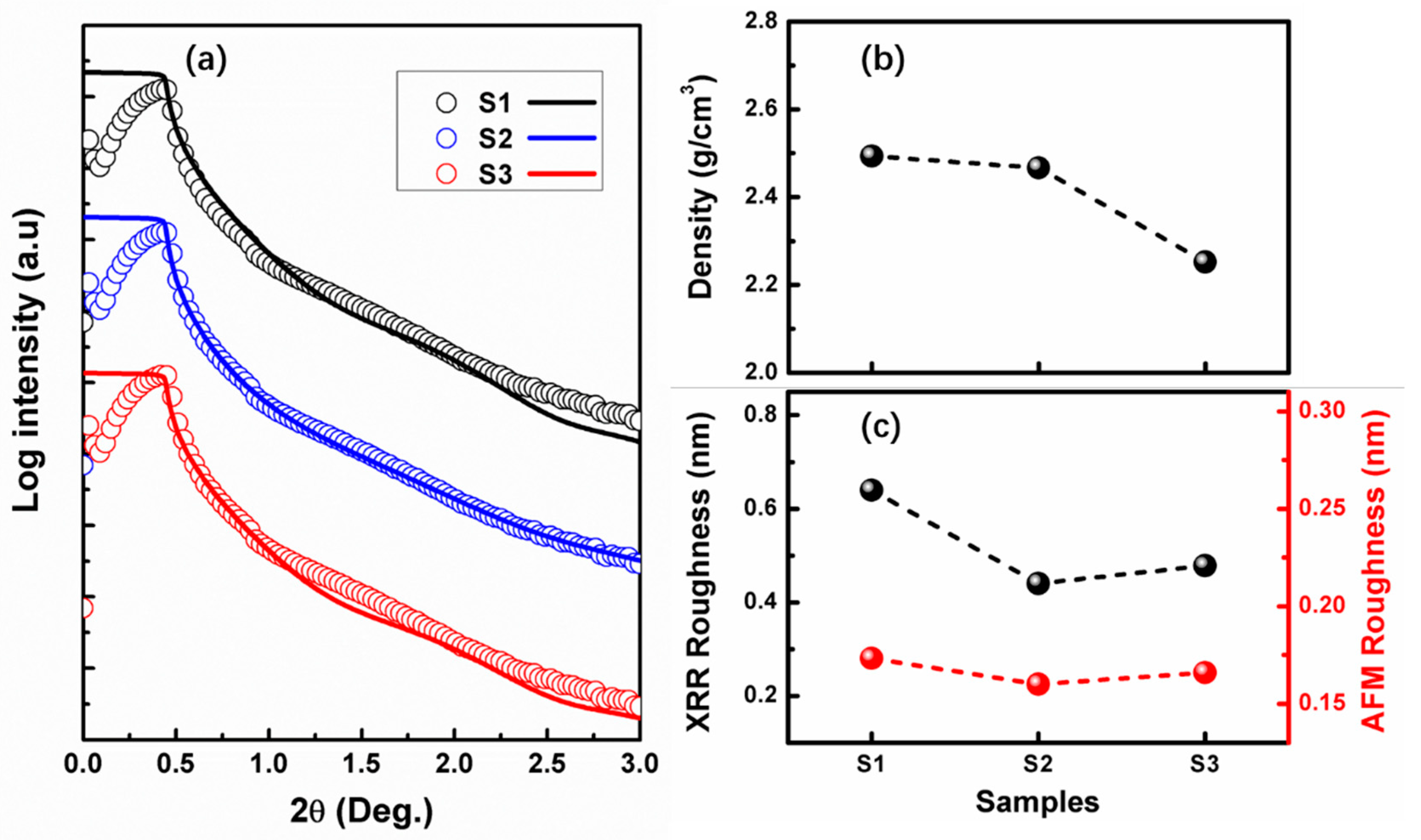
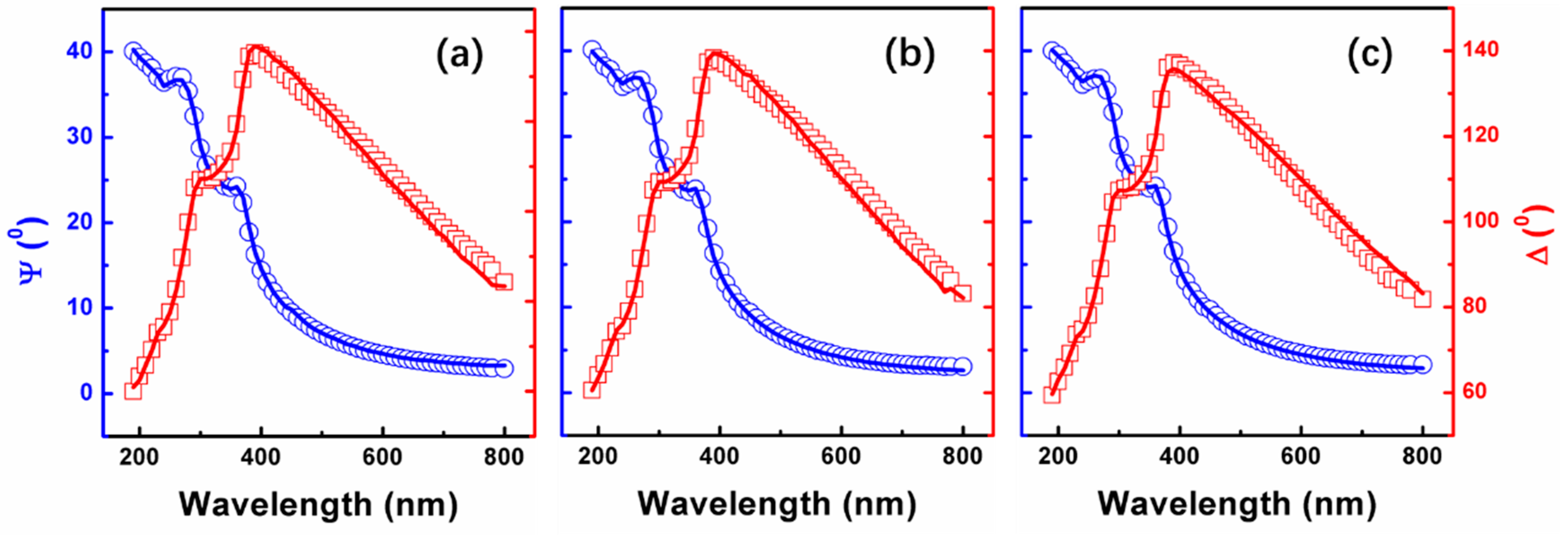
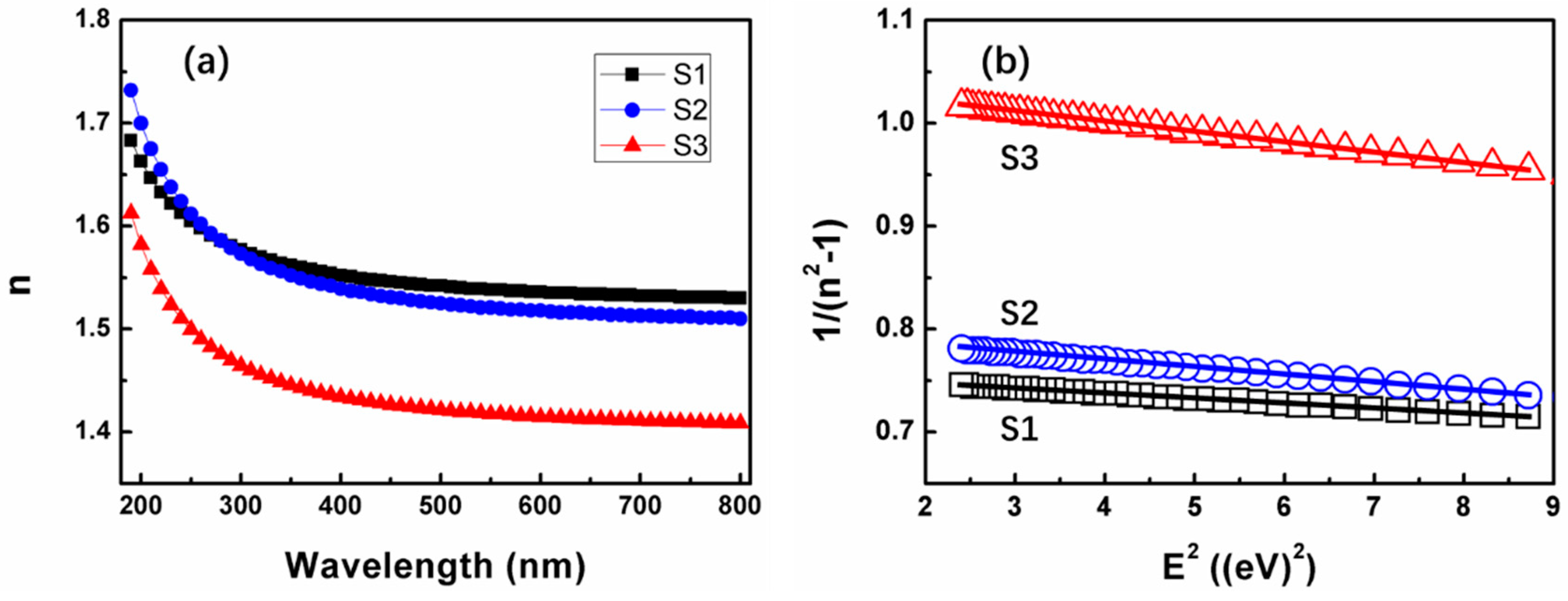
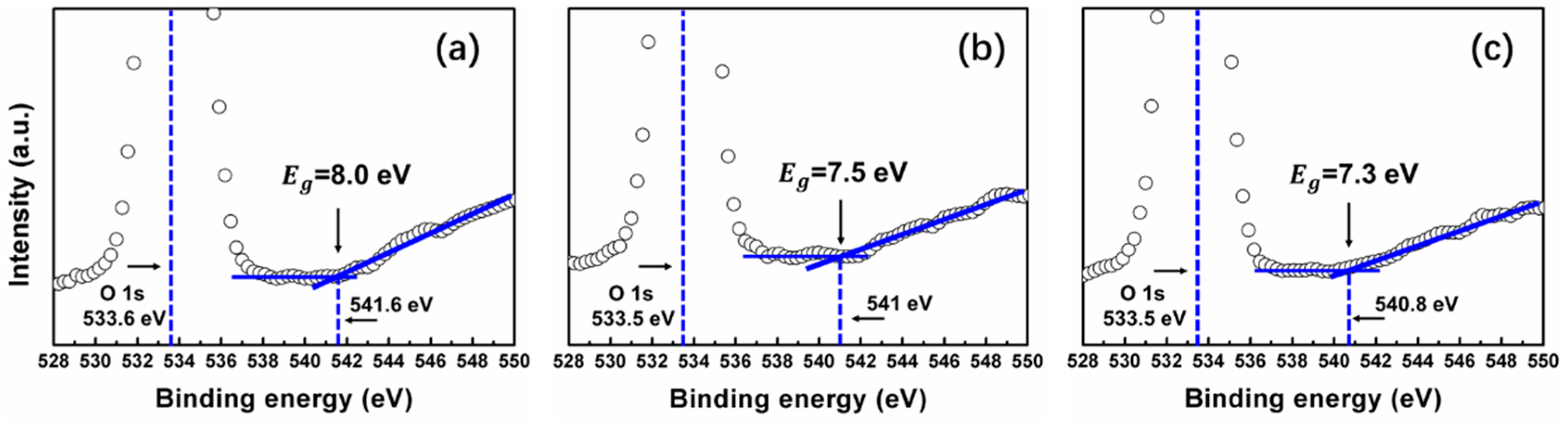
3.2. Properties of SiOx Film with Different Stoichiometry

To further analyze the concentration, microstructure, chemical valence, and composition of the film and elements, the Si 2p and O 1s spectra of the SiOx sample were examined by high-resolution XPS, as shown in Figure 4. From the Si 2p spectra of the S1 film (Figure 4a1), four peaks are observed at 104.4, 103.4, 101.6, and 101 eV, corresponding to the Si-O (SiO2), Si-O (SiO2), Si-OHx (Si(OH)x), and Si-Si (Si substrate) bonds [31], respectively. For the S2 sample, four sub-peaks centered at 104.4, 103.3, 101.4, and 100.8 eV are observed. They are assigned to be the Si-O (SiO2), Si-O (SiO2), Si-OHx (Si(OH)x), and Si-Si (Si substrate) bonds, respectively. It is worth pointing out that the intensity and the area of the Si-OHx and Si-Si related sub-peaks increased compared to the strength in S1 sample, which means more content of silicon-related clusters became residual in the film. For the S3 sample, the four sub-peaks are centered at 104.2, 103.3, 101.2, and 100.6 eV. The intensity and area of the Si-OHx related sub-peak further increased, which is induced by the decrease in O2 plasma duration and flow rate. By comparing the O 1s spectra of S1 (Figure 4a2), S2 (Figure 4b2) and S3 sample (Figure 4c2), it can be found that the O 1s spectra in all three films can be fitted mainly by two sub-peaks located at ~534 eV and ~533.3 eV. For S1, it is 534 eV and 533.3 eV, for S2, it is 534.3 eV and 533.3 eV, then for S3, it is 533.7 eV and 533.2 eV. When we compare these two sub-peaks with the sub-peaks related to Si-O bonds in Si 2p peak (for a better view, they were both marked as the same red and blue color, respectively), we find that they present the same variation tendency in these three samples. Evidently, in Si 2p peaks, the sub-peak related to Si-O bonds with higher binding energy (red line) changed from 104.4 eV to 104.2 eV when reducing the oxygen content in SiOx film. As a matter of fact, the sub-peak related to O-Si bonds with higher binding energy (red line) also shifted from 534 eV to 533.7 eV. Therefore, it is supposed that the two sub-peaks related to O-Si bonds in the O 1s peak (Figure 4a2–c2) correspond with the two sub-peaks related to Si-O bonds of the matching sample found in Si 2p (Figure 4a1–c1). Moreover, the distance of the two sub-peaks related to Si-O bonds decreased from 1.0 eV to 0.9 eV, while, the value of the two sub-peaks related to O-Si bonds decreased from 0.7 to 0.5 eV as well. In addition to these variations, the relative intensity of these two sub-peaks corresponding to high and low binding energy also had the same variation trend both in Si 2p and O 1s. All these results indicate that the chemical binding energy and microstructure are different in these SiOx film with different stoichiometry.
For further analysis, the TEM test was used to verify the microstructure like surface roughness and the interfacial composition of these three films. The surface morphology of the three samples can be observed by the low-resolution TEM images shown in Figure 5a1–c1. It can be seen that all films present a smooth surface. This finding agrees with the surface morphology and roughness data shown in Figure 2c, since all films were deposited at 200 °C. The high-resolution TEM images shown in Figure 5a2–c2 exhibit different film structure. As shown in Figure 5a2, the S1 sample is just composed of one layer, which is obviously the SiO2 film. For S2 sample, two sublayers are detectable in Figure 5b2, layer 1 is assigned to the SiO2 owing to the native oxidation on the substrate surface. It also comes from the contribution of residual oxygen in the reactor chamber. It should be noted that residual oxygen is unavoidable since the vacuum is just about 1 mbar. Therefore, at the beginning of the ALD process, the oxygen flow was unstable and not the value that we desired. As a result, SiO2 was generated more or less on the surface of the Si substrate. After few ALD cycles, the residual oxygen in the chamber ran out. Then, silicon oxides with the desired stoichiometry could be obtained when the oxygen flow began to stabilize. Based on this, layer 2 in Figure 5b2 is assigned to the SiO1.8 layer. Moreover, for the S3 sample shown in Figure 5c2, a bilayers structure can also be found. Same as the S2 sample, the layers 1 and 2 are assigned to SiO2 and SiO1.6, respectively. This finding is in agreement with the variation of the Si-O bonds in the Si 2p spectra and O-Si bonds in the O 1s spectra. To be specific, as seen in Figure 4, both of Si-O and O-Si bonds shift to lower binding energy with the Si/O ratio changing from 2 to 1.6. According to reports in previous research, higher valence of Si ion corresponds to higher binding energy [32,33]. On the basis of this finding, there is reason to believe that a certain amount of Si ion turns to lower valence in S2 and S3 sample. This can be verified both by the Si 2p spectra in Figure 4b1–c1 and the TEM structure in Figure 5b2–c2. Meanwhile, because of the existence of more valence states in S2 and S3 sample, the Si 2p and O 1s spectra in these two samples present broaden profile than the value in S1 sample, as seen in Figure 4.
Figure 6a shows the measured (scatter line) and simulated (solid line) XRR curve of the SiOx film with different stoichiometry. Figure 6b,c shows the film density and roughness obtained by XRR simulation. The density of SiO2 (S1) sample was ~2.49 g/cm3, and it became 2.46 g/cm3 for the SiO1.8 (S2) film. Then, the value decreased to 2.25 g/cm3 for SiO1.6 (S2) film. This result indicated that the mass density of silicon dioxide decreases with the decrease of oxygen concentration, in other words, the film mass density becomes lower for Si rich silicon dioxide (SiO1.6) than SiO2. Meanwhile, surface roughness obtained by XRR and AFM is also shown in Figure 6c. It was found that the surface roughness of all the films prepared in this work is very small, which means that the film is very smooth. It should be noted here that both XRR and AFM data present a similar tendency of variation for roughness. Obviously, the RMS result simulated from XRR data is higher than the value obtained by AFM, which is in agreement with the result reported in other work [34]. As seen from RMS values obtained by XRR, the SiO2 film exhibits the highest RMS roughness value of about 0.64 nm, and the value of the other film is around 0.4–0.5 nm.
In order to achieve in-depth knowledge on the evolution of the optical properties of SiOx film with different stoichiometry, SE measurements have been performed at room temperature immediately after removing the samples from the deposition system to avoid surface contamination. The measured (scatter line) and simulated (solid line) Ψ and Δ of SiOx thin films for angles of incidence 75° are shown in Figure 7. From this data, the refractive index of the SiOx can be deduced through a fitting-based analysis. Because of the excellent transparency of the SiOx in the considered wavelength range, it is valid to use a Cauchy relation to model the refractive index of the SiOx: n ( λ ) = A + B / λ 2 + C / λ 4 . As can be seen in Figure 7, an excellent fit (solid lines) is achieved. Then, the optical constants of SiOx thin film is extracted and obtained from the fitted Ψ and Δ. Figure 8a shows the changes of the refractive index (n) as a function of wavelength in the range of 190–800 nm. Evidently, this fitting procedure yielded a refractive index value (n) of 1.54 at a wavelength of 632.8 nm for SiO2, in agreement with the value reported in the literature [35]. Then for SiO1.8 and SiO1.6, it becomes 1.51 and 1.42, respectively. Therefore, the refractive index of the SiOx film can be affected by varying the oxygen concentration.
The refractive index dispersion n of SiOx film was further fitted by the Wemple-DiDomenico model [36] with the purpose of determining the oscillator energy and strength. The refractive index data can be fitted in the spectra below the band-gap to the single oscillator expression [37]:
n 2 = 1 + E 0 · E d E 0 2 E 2
where E represents the photon energy, E0 measures oscillator energy, and Ed represents dispersion energy, which measures the oscillator strength (the strength of inter-band optical transitions). From linear regression of dependence (n2 − 1)−1 against E2 (as shown in Figure 8b), the parameters E0 and Ed can be calculated. The values of the fitting constants E0 and Ed are given in Table 1. We can see that for SiO2 sample, E0 is ~12.5 eV, Ed is ~16.5 eV. For SiO1.8 sample, E0 is ~10.5 eV, Ed is ~12.8 eV. Then, for SiO1.6 sample, E0 is ~10.4 eV, Ed is ~9.8 eV. The oscillator energy, E0, is an ‘average’ energy gap, as pointed out in many references [38,39,40]. S.H. Wemple et al. [36] found out that E0 is related empirically to the lowest direct energy band-gap Eg by E0 ≈ 1.5 Eg. The values of Eg determined in this way are 8.3, 7.3, and 6.9 eV for SiO2, SiO1.8, and SiO1.6, respectively. Meanwhile, Eg of these SiOx film was also determined by XPS O 1s data, which has been reported by many scientists [41,42,43]. As shown in Figure 9, a representative high-resolution scan of the O 1s core level of SiO2, SiO1.8, and SiO1.6 film are used to determine the energy band-gap of these three films. We can notice that the Eg is 8, 7.5, and 7.3 eV for SiO2, SiO1.8, and SiO1.6 film, respectively. As shown in Table 1, the energy band-gap obtained by O 1s peak is very close to the value obtained by the E0 simulation above. This result confirms that the energy band-gap of SiOx films decrease with decreasing oxygen composition.
For the dispersion energy an empirical relation is established [36]: Ed = βNcNeZa, where β is a constant, according to Wemple, β has a value of 0.37~0.04 eV. Nc is the coordination number of the nearest neighboring cation to the anion, and Za is the formal chemical valency of the anion, then Ne is the total number of valence electrons per anion [39]. For SiO2, Ne = [(4 valence electrons)·(1 silicon cation) + (6 valence electrons)·(2 oxygen anions)]/2 = 8, and Za = 2. For SiO, Ne = [(4 valence electrons)·(1 silicon cation) + (6 valence electrons)·(1 oxygen anions)]/1 = 10, and Za = 2. Thus, Nc can be calculated from the relationship: Nc = Ed/βNe Za. It is noted that the values of Ed and Nc decreases with the decrease of oxygen concentration in SiOx film. So, we can conclude that SiOx film has a more amorphous structure than SiO2 film. This result correlates with the fact that the SiOx film is less dense and has a lower refractive index [44]. In fact, Figure 6b and Figure 8a demonstrate that the variation of film density and refractive index agrees with this result perfectly. Furthermore, the decrease of Ed from SiO2 to SiOx sample is also supposed to relate to the effective number of valence electrons, the variation of Si-O and Si-Si bonds, as shown in Figure 4.
Moreover, the long-wavelength limit of the refractive index, n(0), is given by [44]: n2(0) = 1+ Ed/E0. Then n(0) is estimated to be 1.52, 1.49, and 1.39 for SiO2, SiO1.8, and SiO1.6, respectively, as seen in Table 1. For comparison, the refractive index at 632.8 nm obtained by SE analysis are also listed in Table 1. It is easy to find that the value of n(0) is very close to the refractive index at 632.8 nm, except for a little smaller. The excellent agreement of these results improved the correctness of the model.

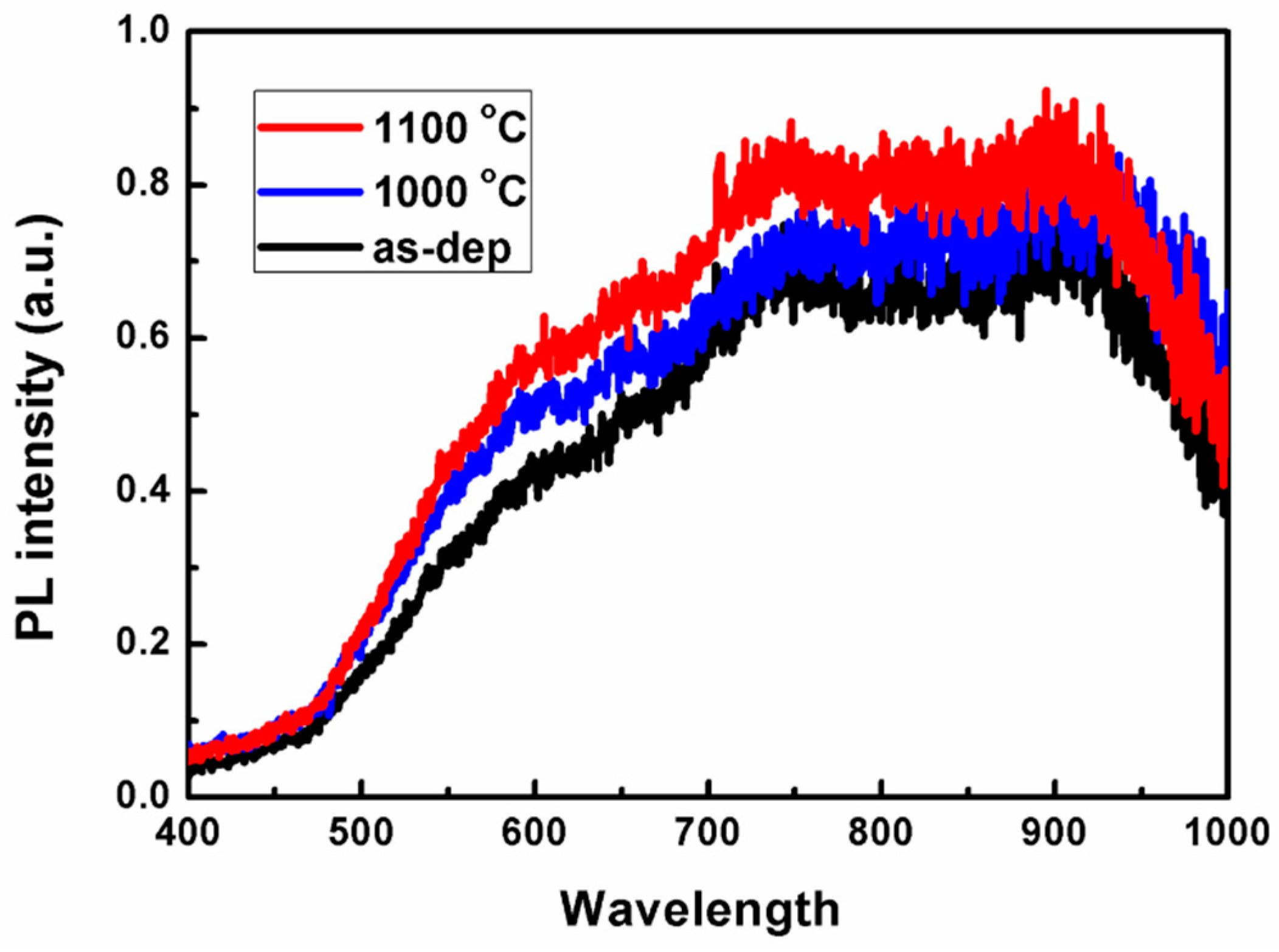
3.3. Photoluminescence Properties of SiO1.6/SiO2 Super-Lattice

To exam the luminescence property of the Si rich SiOx film prepared in this work, SiOx/SiO2 super-lattice with x = 1.6 was fabricated. The super-lattice consisted of 22 SiO1.6/SiO2 bilayers, and the nominal thickness of SiO1.6 layer was ~1.5 nm, while the SiO2 layer was fixed at ~3 nm, so the total film thickness was about 100 nm. In order to form the Si-NCs in the SiO2 matrix, thermal annealing was performed in a rapid thermal annealing furnace under nitrogen atmosphere with ramp rates of about 25 °C/s for phase separation and crystallization. In this work, the sample was annealed at 1000 and 1100 °C for 10 s.
Figure 10 compares the room-temperature PL spectra of the SiO1.6/SiO2 super-lattice before and after RTP annealing with different temperature. All of the spectra show the similar luminescence profiles, and the PL maximum position does not show any notable features with annealing temperatures, except for an increase in the PL intensity. In detail, three peaks all have a broader profile ranging from 550 nm to 1000 nm, and two small peaks presents around 750 nm and 920 nm. It seems that the spectra is superimposed by some small peaks, for example, three sub-peaks with gaussian shape located at 600, 750, and 920 nm could form a spectra like this. This result presents a familiar PL spectra for Si-NCs in SiOx/SiO2 super-lattice deposited by other techniques in previous reports [11,45,46,47,48]. The weak and inapparent luminescence properties of the super-lattice implied that there was not enough Si-NCs formed in SiO2 matrix. On one hand, it is supposed that the annealing temperature and time are not sufficient to form Si-NCs compared with the conditions in the previous report [49]. On the other hand, the SiO1.6 layer was not Si-rich enough to form considerable Si-NCs when high temperature annealing. Specifically, the high temperature annealing of such initially amorphous SiOx films results in phase separation described by [9],
SiO x x 2 SiO 2 + ( 1 x 2 ) Si
in SiOx clusters. The phase separation of the SiOx automatically ensures that the nucleated Si nanocrystals/nanoclusters are separated from each other by a SiO2 shell. Based on the theory above, it is just 20% of SiOx cluster turned to Si nanocrystals when x = 1.6. Also, as reported in previous articles [50], an increase in the stoichiometry parameter x to 1.63 in SiOx/SiO2 matrix resulted in a drastically reduced density of nanocrystals correlated with a strong decrease in PL intensity. Based on Equation (2), the thickness of the oxide between the Si nanoclusters depends on the stoichiometry of the SiOx as well. The crystallization of SiOx film resulted in randomly distributed nanocrystals with an average size that depends on the original stoichiometry. So both the thickness of SiOx and SiO2 layer also play a role in this property, which should be systematically studying in further research.

4. Conclusions

In this study, the SiOx thin film with different stoichiometry was successfully deposited with TDMAS and O2 plasma by using PEALD. In order to realize this target, the deposition parameter was firstly studied, and the effect of deposition temperature, plasma pulse time, and gas flow on growth rate was obtained. Then, SiOx thin films with different stoichiometry were fabricated by optimizing the precursor pulse time and O2 gas flow. Meanwhile, the micro-structure, chemical, and optical properties were systematically investigated by AFM, TEM, XRR, SE, and XPS measurements. It was found that the mass density, refractive index, and optical energy band-gap of SiOx film are all lower than SiO2 film. Furthermore, SiO1.6/SiO2 superlattice with 150 nm thickness was fabricated based on the deposition parameters obtained above. The photoluminescence test shows that the SiO1.6/SiO2 super-lattice presents a weak and indistinctive peak before and after high temperature annealing, implying that the SiO1.6 film is still not Si rich enough. Further research is worth exploring to obtain the SiOx film with a smaller x value by optimizing PEALD parameters.

Author Contributions

Conceptualization, H.-P.M. and H.-L.L.; Data curation, H.-P.M., J.-G.Y., L.-Y.Z., W.H., G.-J.Y. and J.-J.F.; Formal analysis, J.-H.Y. and T.-C.J.; investigation, H.-P.M.; project administration, H.-L.L.; supervision, H.-L.L.; H.-P.M. wrote the paper.

Funding

This research was funded by the National Key R&D Program of China (No. 2016YFE0110700), National Natural Science Foundation of China (Nos. U1632121, 11804055, 51861135105 and 61874034), and China Postdoctoral Science Foundation (No. 2018M631997).

Acknowledgments

The authors want to thank Pei-Hong Cheng from Shanghai Tech University for her great help during XPS measurements.

Conflicts of Interest

The authors declare no conflicts of interest.

References

  1. Heitmann, J.; Scholz, R.; Schmidt, M.; Zacharias, M. Size controlled nc-Si synthesis by SiO/SiO2 superlattices. J. Cryst. Solids 2002, 299, 1075–1078. [Google Scholar] [CrossRef]
  2. Huh, C.; Kim, B.K.; Park, B.J.; Jang, E.H.; Kim, S.H. Enhancement in electron transport and light emission efficiency of a Si nanocrystal light-emitting diode by a SiCN/SiC superlattice structure. Nanoscale Res. Lett. 2013, 8, 14. [Google Scholar] [CrossRef] [PubMed] [Green Version]
  3. Zhigunov, D.M.; Sarikov, A.; Chesnokov, Y.M.; Vasiliev, A.L.; Zakharov, N.; Kashkarov, P.K. Thickness and temperature depending intermixing of SiOx/SiO2 and SiOxNy/SiO2 superlattices: Experimental observation and thermodynamic modeling. Appl. Phys. Lett. 2016, 108, 223102. [Google Scholar] [CrossRef]
  4. Canham, L.T. Silicon quantum wire array fabrication by electrochemical and chemical dissolution of wafers. Appl. Phys. Lett. 1990, 57, 1046–1048. [Google Scholar] [CrossRef]
  5. Kanemitsu, Y. Luminescence properties of nanometer-sized Si crystallites: Core and surface states. Phys. Rev. B 1994, 49, 16845–16848. [Google Scholar] [CrossRef]
  6. Chen, L.-Y.; Chen, W.-H.; Hong, F.C.-N. Visible electroluminescence from silicon nanocrystals embedded in amorphous silicon nitride matrix. Appl. Phys. Lett. 2005, 86, 193506. [Google Scholar] [CrossRef]
  7. Di Bartolomeo, A.; Rücker, H.; Schley, P.; Fox, A.; Lischke, S.; Na, K.-Y. A single-poly EEPROM cell for embedded memory applications. Solid State Electron. 2009, 53, 644–648. [Google Scholar] [CrossRef]
  8. Tiwari, S.; Rana, F.; Hanafi, H.; Hartstein, A.; Crabbé, E.F.; Chan, K. A silicon nanocrystals based memory. Appl. Phys. Lett. 1996, 68, 1377–1379. [Google Scholar] [CrossRef]
  9. Zacharias, M.; Heitmann, J.; Scholz, R.; Kahler, U.; Schmidt, M.; Bläsing, J. Size-controlled highly luminescent silicon nanocrystals: A SiO/SiO2 superlattice approach. Appl. Phys. Lett. 2002, 80, 661–663. [Google Scholar] [CrossRef]
  10. Gutsch, S.; Hiller, D.; Laube, J.; Zacharias, M.; Kubel, C. Observing the morphology of single-layered embedded silicon nanocrystals by using temperature-stable TEM membranes. Beilstein J. Nanotechnol. 2015, 6, 964–970. [Google Scholar] [CrossRef] [Green Version]
  11. Yi, L.; Scholz, R.; Zacharias, M. Size and density control of Si-nanocrystals realized by SiOx/SiO2 superlattice. J. Lumin. 2007, 122–123, 750–752. [Google Scholar] [CrossRef]
  12. Godefroo, S.; Hayne, M.; Jivanescu, M.; Stesmans, A.; Zacharias, M.; Lebedev, O.I.; Van Tendeloo, G.; Moshchalkov, V.V. Classification and control of the origin of photoluminescence from Si nanocrystals. Nat. Nanotechnol. 2008, 3, 174–178. [Google Scholar] [CrossRef] [PubMed] [Green Version]
  13. Hiller, D.; Jivanescu, M.; Stesmans, A.; Zacharias, M. Pb(0) centers at the Si-nanocrystal/SiO2 interface as the dominant photoluminescence quenching defect. J. Appl. Phys. 2010, 107, 084309. [Google Scholar] [CrossRef]
  14. Konig, D.; Gutsch, S.; Gnaser, H.; Wahl, M.; Kopnarski, M.; Gottlicher, J.; Steininger, R.; Zacharias, M.; Hiller, D. Location and Electronic Nature of Phosphorus in the Si Nanocrystal-SiO2 System. Sci. Rep. 2015, 5, 9702. [Google Scholar] [CrossRef] [PubMed]
  15. Goncharova, L.V.; Nguyen, P.H.; Karner, V.L.; D’Ortenzio, R.; Chaudhary, S.; Mokry, C.R.; Simpson, P.J. Si quantum dots in silicon nitride: Quantum confinement and defects. J. Appl. Phys. 2015, 118, 224302. [Google Scholar] [CrossRef]
  16. Hiller, D.; Zelenina, A.; Gutsch, S.; Dyakov, S.A.; López-Conesa, L.; López-Vidrier, J.; Estradé, S.; Peiró, F.; Garrido, B.; Valenta, J.; et al. Absence of quantum confinement effects in the photoluminescence of Si3N4–embedded Si nanocrystals. J. Appl. Phys. 2014, 115, 204301. [Google Scholar] [CrossRef]
  17. Suwa, Y.; Saito, S. Intrinsic optical gain of ultrathin silicon quantum wells from first-principles calculations. Phys. Rev. B 2009, 79, 233308. [Google Scholar] [CrossRef]
  18. Hartel, A.M.; Hiller, D.; Gutsch, S.; Löper, P.; Estradé, S.; Peiró, F.; Garrido, B.; Zacharias, M. Formation of size-controlled silicon nanocrystals in plasma enhanced chemical vapor deposition grown SiOxNy/SiO2 superlattices. Thin Solid Films 2011, 520, 121–125. [Google Scholar] [CrossRef]
  19. Liao, W.; Zeng, X.; Yao, W.; Wen, X. Photoluminescence and carrier transport mechanisms of silicon-rich silicon nitride light emitting device. Appl. Surf. Sci. 2015, 351, 1053–1059. [Google Scholar] [CrossRef]
  20. Janz, S.; Löper, P.; Schnabel, M. Silicon nanocrystals produced by solid phase crystallisation of superlattices for photovoltaic applications. Mater. Sci. Eng. B-Solid 2013, 178, 542–550. [Google Scholar] [CrossRef]
  21. Nguyen, P.D.; Kepaptsoglou, D.M.; Ramasse, Q.M.; Sunding, M.F.; Vestland, L.O.; Finstad, T.G.; Olsen, A. Impact of oxygen bonding on the atomic structure and photoluminescence properties of Si-rich silicon nitride thin films. J. Appl. Phys. 2012, 112, 073514. [Google Scholar] [CrossRef]
  22. Di, D.; Xu, H.; Perez-Wurfl, I.; Green, M.A.; Conibeer, G. Optical characterisation of silicon nanocrystals embedded in SiO2/Si3N4 hybrid matrix for third generation photovoltaics. Nanoscale Res. Lett. 2011, 6, 612. [Google Scholar] [CrossRef] [PubMed]
  23. Shih, C.F.; Hsiao, C.Y.; Su, K.W. Enhanced white photoluminescence in silicon-rich oxide/SiO2 superlattices by low-energy ion-beam treatment. Opt. Express 2013, 21, 15888–15895. [Google Scholar] [CrossRef] [PubMed]
  24. Kim, M.; Sundararaman, R.; Tiwari, S.; Lee, J.-W. Charge Trapping Devices Using a Bilayer Oxide Structure. J. Nanosci. Nanotechnol. 2012, 12, 423–427. [Google Scholar] [CrossRef] [PubMed]
  25. O’Donoghue, R.; Rechmann, J.; Aghaee, M.; Rogalla, D.; Becker, H.W.; Creatore, M.; Wieck, A.D.; Devi, A. Low temperature growth of gallium oxide thin films via plasma enhanced atomic layer deposition. Dalton Trans. 2017, 46, 16551–16561. [Google Scholar] [CrossRef] [PubMed]
  26. Biyikli, N.; Haider, A. Atomic layer deposition: An enabling technology for the growth of functional nanoscale semiconductors. Semicond. Sci. Technol. 2017, 32, 093002. [Google Scholar] [CrossRef]
  27. Johnson, R.W.; Hultqvist, A.; Bent, S.F. A brief review of atomic layer deposition: From fundamentals to applications. Mater. Today 2014, 17, 236–246. [Google Scholar] [CrossRef]
  28. Goto, H.; Shibahara, K.; Yokoyama, S. Atomic layer controlled deposition of silicon nitride with self-limiting mechanism. Appl. Phys. Lett. 1996, 68, 3257–3259. [Google Scholar] [CrossRef]
  29. Knoops, H.C.; Braeken, E.M.; de Peuter, K.; Potts, S.E.; Haukka, S.; Pore, V.; Kessels, W.M. Atomic Layer Deposition of Silicon Nitride from Bis(tert-butylamino)silane and N2 Plasma. ACS Appl. Mater. Interfaces 2015, 7, 19857–19862. [Google Scholar] [CrossRef]
  30. Kim, Y.; Provine, J.; Walch, S.P.; Park, J.; Phuthong, W.; Dadlani, A.L.; Kim, H.J.; Schindler, P.; Kim, K.; Prinz, F.B. Plasma-Enhanced Atomic Layer Deposition of SiN-AlN Composites for Ultra Low Wet Etch Rates in Hydrofluoric Acid. ACS Appl. Mater. Interfaces 2016, 8, 17599–17605. [Google Scholar] [CrossRef]
  31. Alam, A.U.; Howlader, M.M.R.; Deen, M.J. Oxygen Plasma and Humidity Dependent Surface Analysis of Silicon, Silicon Dioxide and Glass for Direct Wafer Bonding. ECS J. Solid State Sci. Technol. 2013, 2, P515–P523. [Google Scholar] [CrossRef]
  32. Laube, J.; Gutsch, S.; Hiller, D.; Bruns, M.; Kübel, C.; Weiss, C.; Zacharias, M. Formation of size controlled silicon nanocrystals in nitrogen free silicon dioxide matrix prepared by plasma enhanced chemical vapor deposition. J. Appl. Phys. 2014, 116, 223501. [Google Scholar] [CrossRef]
  33. Yang, D.Q.; Gillet, J.N.; Meunier, M.; Sacher, E. Room temperature oxidation kinetics of Si nanoparticles in air, determined by X-ray photoelectron spectroscopy. J. Appl. Phys. 2005, 97, 024303. [Google Scholar] [CrossRef]
  34. Chen, H.Y.; Lu, H.L.; Chen, J.X.; Zhang, F.; Ji, X.M.; Liu, W.J.; Yang, X.F.; Zhang, D.W. Low-Temperature One-Step Growth of AlON Thin Films with Homogenous Nitrogen-Doping Profile by Plasma-Enhanced Atomic Layer Deposition. ACS Appl. Mater. Interfaces 2017, 9, 38662–38669. [Google Scholar] [CrossRef] [PubMed]
  35. Yang, W.; Fronk, M.; Geng, Y.; Chen, L.; Sun, Q.Q.; Gordan, O.D.; Zhou, P.; Zahn, D.R.; Zhang, D.W. Optical properties and bandgap evolution of ALD HfSiOx films. Nanoscale Res. Lett. 2015, 10, 32. [Google Scholar] [CrossRef] [PubMed]
  36. Wemple, S.H.; DiDomenico, M. Behavior of the Electronic Dielectric Constant in Covalent and Ionic Materials. Phys. Rev. B 1971, 3, 1338–1351. [Google Scholar] [CrossRef]
  37. Wemple, S.H. Refractive-Index Behavior of Amorphous Semiconductors and Glasses. Phys. Rev. B 1973, 7, 3767–3777. [Google Scholar] [CrossRef]
  38. Gonzalez-Leal, J.M.; Marquez, E.; Bernal-Oliva, A.M.; Ruiz-Perez, J.J.; Jimenez-Garay, R. Derivation of the optical constants of thermally-evaporated uniform films of binary chalcogenide glasses using only their reflection spectra. Thin Solid Films 1998, 317, 223–227. [Google Scholar] [CrossRef]
  39. Márquez, E.; Ramírez-malo, J.B.; Villares, P.; Jiménez-Garay, R.; Swanepoel, R. Optical characterization of wedge-shaped thin films of amorphous arsenic trisulphide based only on their shrunk transmission spectra. Thin Solid Films 1995, 254, 83–91. [Google Scholar] [CrossRef]
  40. Tanaka, K. Optical properties and photoinduced changes in amorphous AsxS1001-x films. Thin Solid Films 1980, 66, 271–279. [Google Scholar] [CrossRef]
  41. Zhang, F.; Saito, K.; Tanaka, T.; Nishio, M.; Arita, M.; Guo, Q. Wide bandgap engineering of (AlGa)2O3 films. Appl. Phys. Lett. 2014, 105, 162107. [Google Scholar] [CrossRef]
  42. Kamimura, T.; Sasaki, K.; Hoi Wong, M.; Krishnamurthy, D.; Kuramata, A.; Masui, T.; Yamakoshi, S.; Higashiwaki, M. Band alignment and electrical properties of Al2O3/β-Ga2O3 heterojunctions. Appl. Phys. Lett. 2014, 104, 192104. [Google Scholar] [CrossRef]
  43. Nichols, M.T.; Li, W.; Pei, D.; Antonelli, G.A.; Lin, Q.; Banna, S.; Nishi, Y.; Shohet, J.L. Measurement of bandgap energies in low-k organosilicates. J. Appl. Phys. 2014, 115, 094105. [Google Scholar] [CrossRef] [Green Version]
  44. Mardare, D.; Hones, P. Optical dispersion analysis of TiO2 thin films based on variable-angle spectroscopic ellipsometry measurements. Mater. Sci. Eng. B 1999, 68, 42–47. [Google Scholar] [CrossRef]
  45. Yi, L.X.; Heitmann, J.; Scholz, R.; Zacharias, M. Si rings, Si clusters, and Si nanocrystals—Different states of ultrathin SiOx layers. Appl. Phys. Lett. 2002, 81, 4248–4250. [Google Scholar] [CrossRef]
  46. Yi, L.X.; Heitmann, J.; Scholz, R.; Zacharias, M. Phase separation of thin SiO layers in amorphous SiO/SiO2 superlattices during annealing. J. Phys. Condens. Matter 2003, 15, S2887–S2895. [Google Scholar] [CrossRef]
  47. Li, D.; Chen, Y.B.; Ren, Y.; Zhu, J.; Zhao, Y.Y.; Lu, M. A multilayered approach of Si/SiO to promote carrier transport in electroluminescence of Si nanocrystals. Nanoscale Res. Lett. 2012, 7, 200. [Google Scholar] [CrossRef] [PubMed] [Green Version]
  48. Heitmann, J.; Muller, F.; Yi, L.X.; Zacharias, M.; Kovalev, D.; Eichhorn, F. Excitons in Si nanocrystals: Confinement and migration effects. Phys. Rev. B 2004, 69, 195309. [Google Scholar] [CrossRef]
  49. López-Vidrier, J.; Hernández, S.; Hiller, D.; Gutsch, S.; López-Conesa, L.; Estradé, S.; Peiró, F.; Zacharias, M.; Garrido, B. Annealing temperature and barrier thickness effect on the structural and optical properties of silicon nanocrystals/SiO2 superlattices. J. Appl. Phys. 2014, 116, 133505. [Google Scholar] [CrossRef]
  50. Kahler, U.; Hofmeister, H. Visible light emission from Si nanocrystalline composites via reactive evaporation of SiO. Opt. Mater. 2001, 17, 83–86. [Google Scholar] [CrossRef]
Figure 1. (a) Parameters of one atomic layer deposition (ALD) cycle of the SiOx growth utilized in this work. Growth rate of SiOx films in dependence on (b) temperature, (c) plasma pulse time (with 2 s tris(dimethylamino)silane (TDMAS) pulse time), and (d) TDMAS pulse time (with 2 s plasma pulse time).
Nanomaterials 09 00055 g001
Figure 2. Three-dimensional and two-dimensional AFM images of SiO2 films deposited at (a) 100 °C, (b) 150 °C, (c) 200 °C, and (d) 250 °C, respectively.
Nanomaterials 09 00055 g002
Figure 3. X-ray photo-electron spectroscopy (XPS) survey scans of SiOx film with different stoichiometry.
Nanomaterials 09 00055 g003
Figure 4. XPS analyses of SiO2 (a1,a2), SiO1.8 (b1,b2), and SiO1.6 (c1,c2) samples.
Nanomaterials 09 00055 g004
Figure 5. TEM images of SiO2 (a1,a2), SiO1.8 (b1,b2), and SiO1.6 (c1,c2) samples on Si substrate.
Nanomaterials 09 00055 g005
Figure 6. (a) Measured and simulated X-ray reflection (XRR) curves of three kinds of SiOx film. (b) Density, and (c) root mean-square (RMS) roughness of these films obtained by XRR simulation.
Nanomaterials 09 00055 g006
Figure 7. Ellipsometry measured and simulated Ψ (blue line) and Δ (red line) for (a) S1(SiO2), (b) S2(SiO1.8), and (c) S3(SiO1.6) samples.
Nanomaterials 09 00055 g007
Figure 8. (a) Refractive index and of SiOx thin films as a function of the wavelength, (b) dependence of 1/(n2 − 1) as a function of square photon energy obtained from SE (symbols) and linear fit of this data (solid lines) according to Wemple-DiDomenico model [36].
Nanomaterials 09 00055 g008
Figure 9. The determination of Eg through the O 1s peak analysis through XPS measurement for samples (a) SiO2, (b) SiO1.8, and (c) SiO1.6.
Nanomaterials 09 00055 g009
Figure 10. Photoluminescence spectra of the as-deposited and annealed SiO1.6/SiO2 superlattice.
Nanomaterials 09 00055 g010
Table 1. Characteristics of the studied samples a.
SampleE0/Ed(E0Ed)−1E0EdEgEg (by O 1s)n(0)n/(632.8 nm)
S1 (SiO2)0.7570.004812.5216.548.38.01.521.54
S2 (SiO1.8)0.8210.007410.5312.837.07.51.491.51
S3 (SiO1.6)1.0620.009910.379.756.97.31.391.42
a Single oscillator and dispersion energies E0 and Ed, respectively, the optical energy band-gap, Eg, simulated by E0 and by O 1s peak, refractive index in the long-wavelength limit n(0), and the refractive index n at 632.8 nm from Figure 8a.

