Article

Investigation of the Heteroepitaxial Process Optimization of Ge Layers on Si (001) by RPCVD
1
Key Laboratory of Microelectronic Devices & Integrated Technology, Institute of Microelectronics, Chinese Academy of Sciences, Beijing 100029, China
2
Institute of Microelectronics, University of Chinese Academy of Sciences, Beijing 100049, China
3
Department of Materials and Nano Physics, School of Information and Communication Technology, KTH Royal Institute of Technology, Isafjordsgatan 22, Kista, SE-164 40, Sweden
4
Research and Development Center of Optoelectronic Hybrid IC, Guangdong Greater Bay Area Institute of Integrated Circuit and System, Guangzhou 510535, China
5
Department of Electronics Design, Mid Sweden University, Holmgatan 10, 85170 Sundsvall, Sweden
*
Authors to whom correspondence should be addressed.
Nanomaterials 2021, 11(4), 928; https://doi.org/10.3390/nano11040928
Submission received: 1 March 2021 / Revised: 19 March 2021 / Accepted: 30 March 2021 / Published: 6 April 2021

Abstract

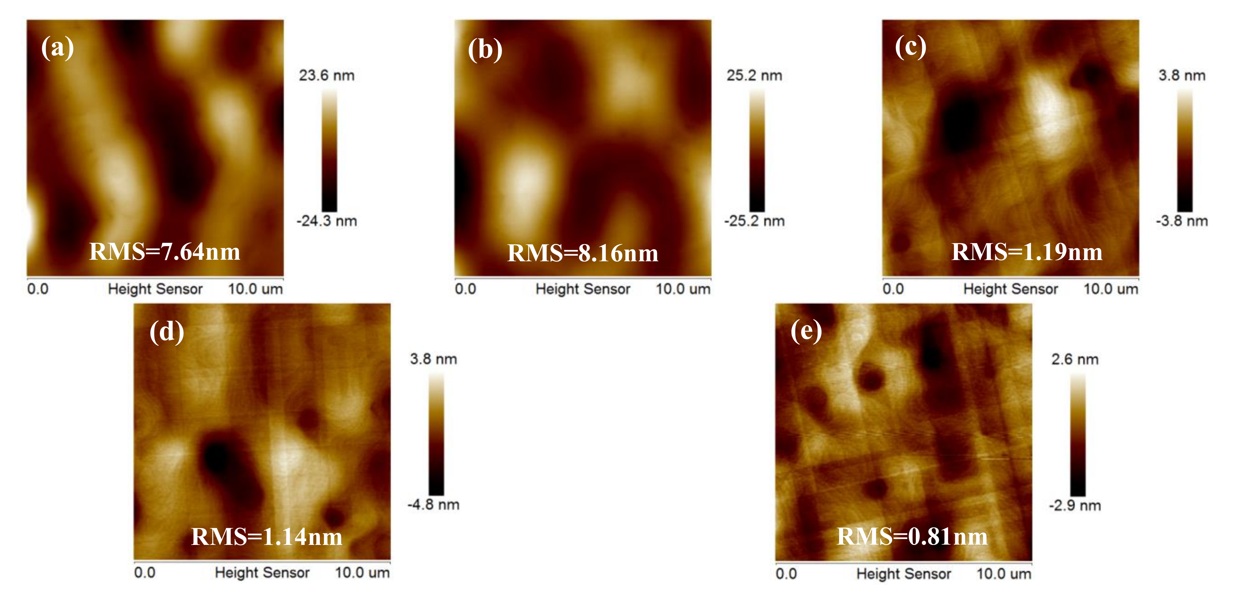
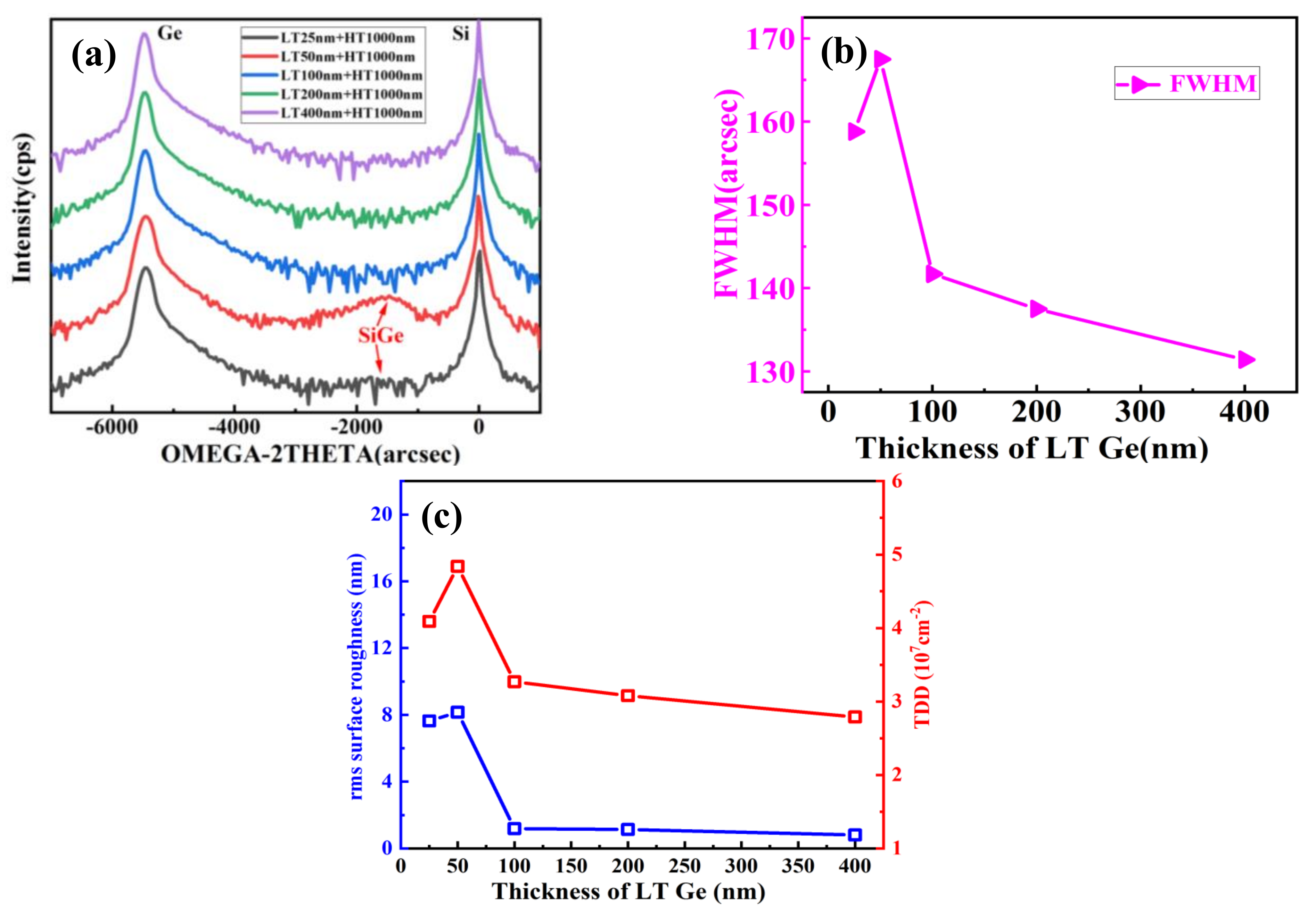
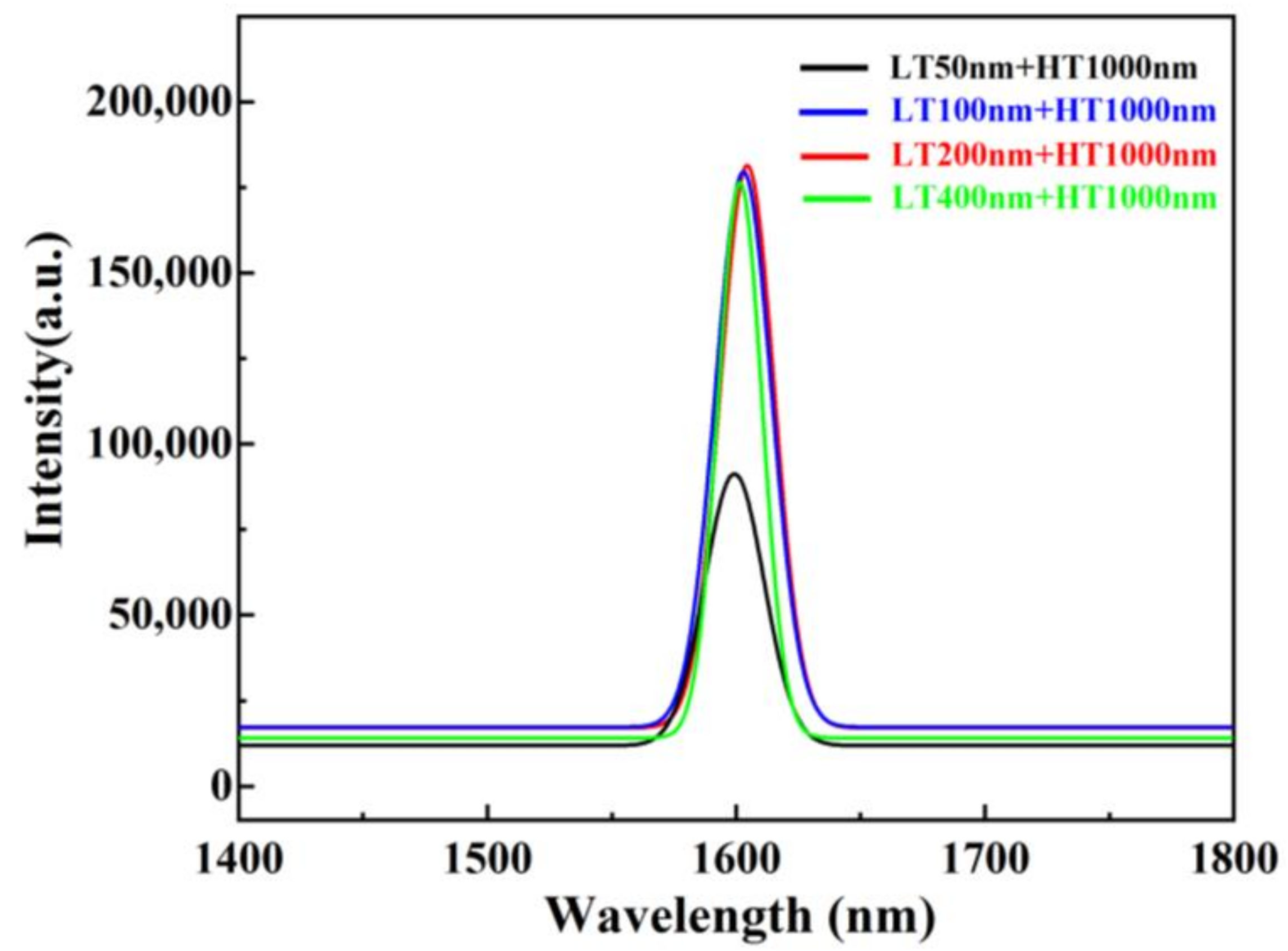
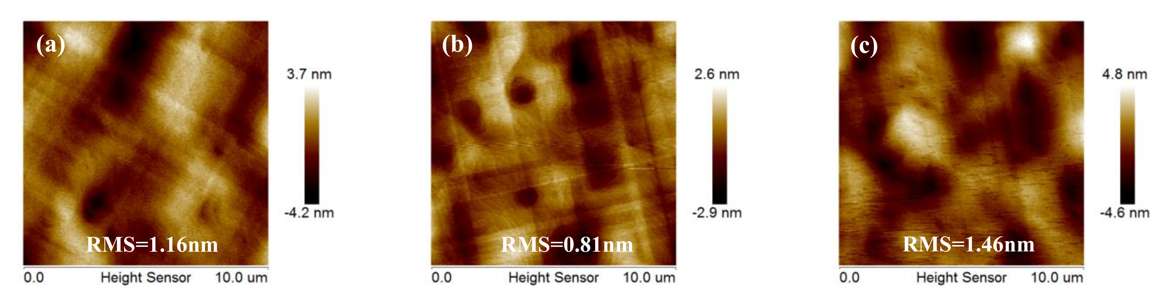
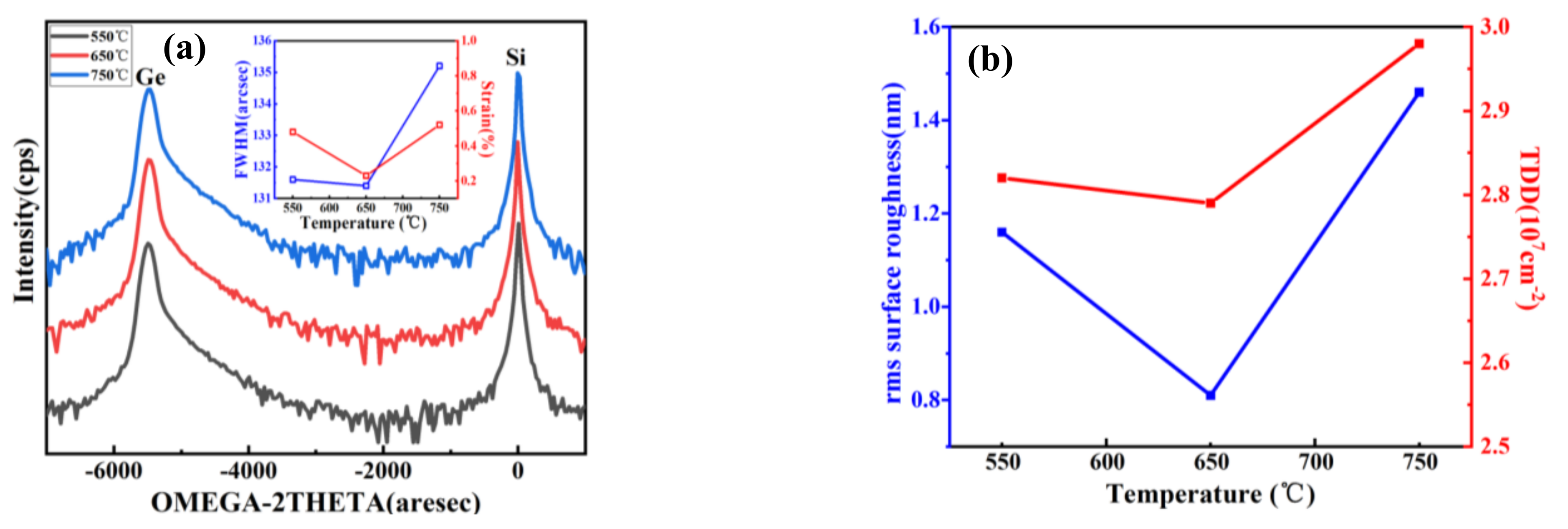
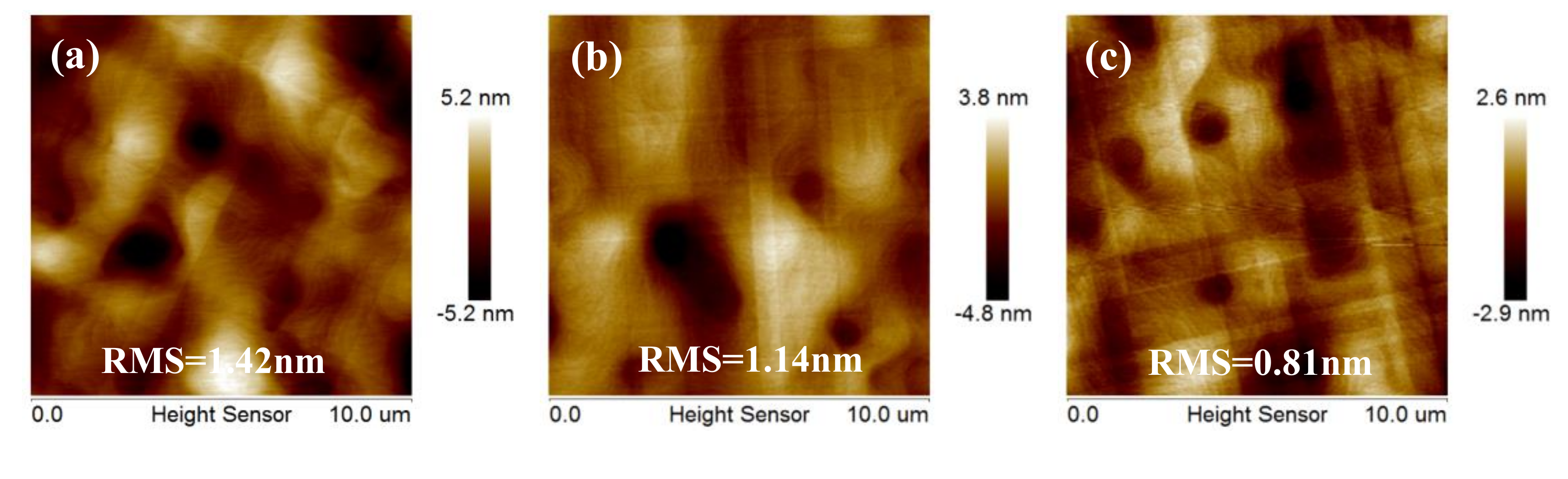
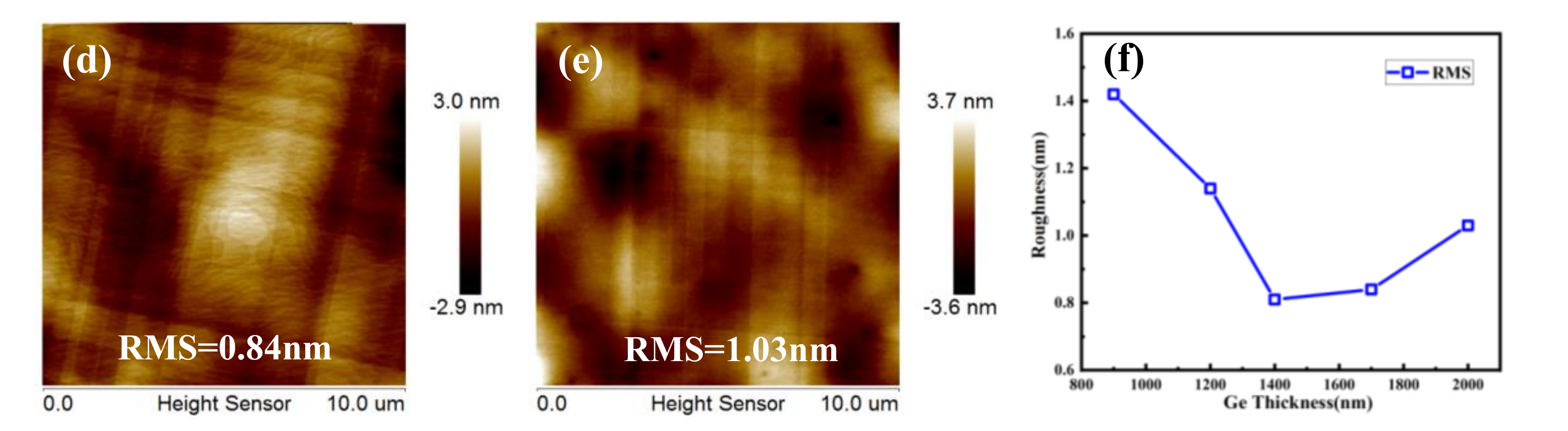
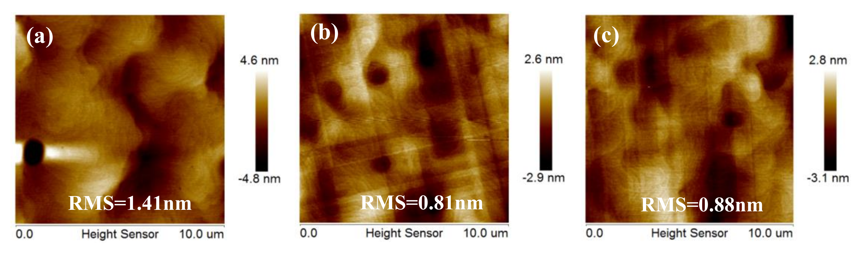
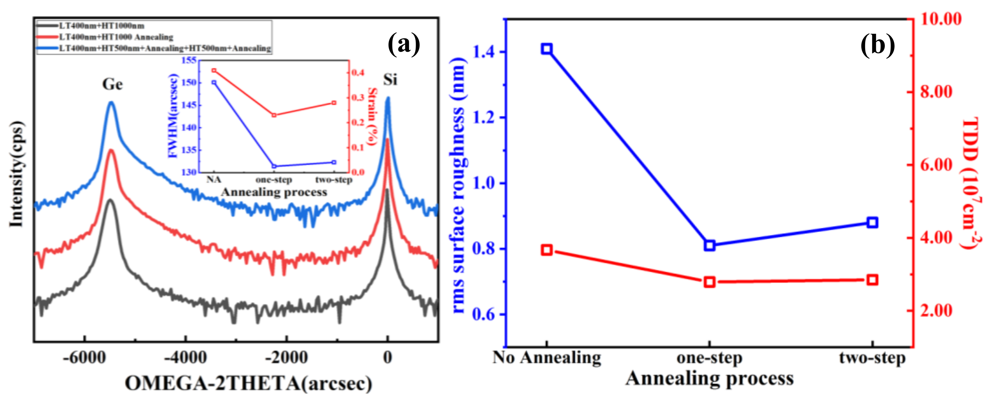
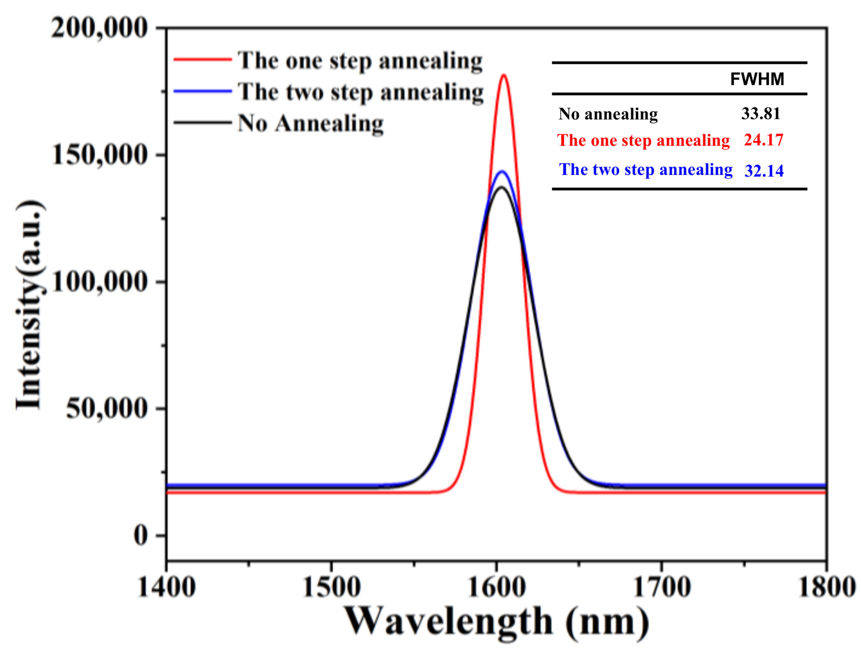
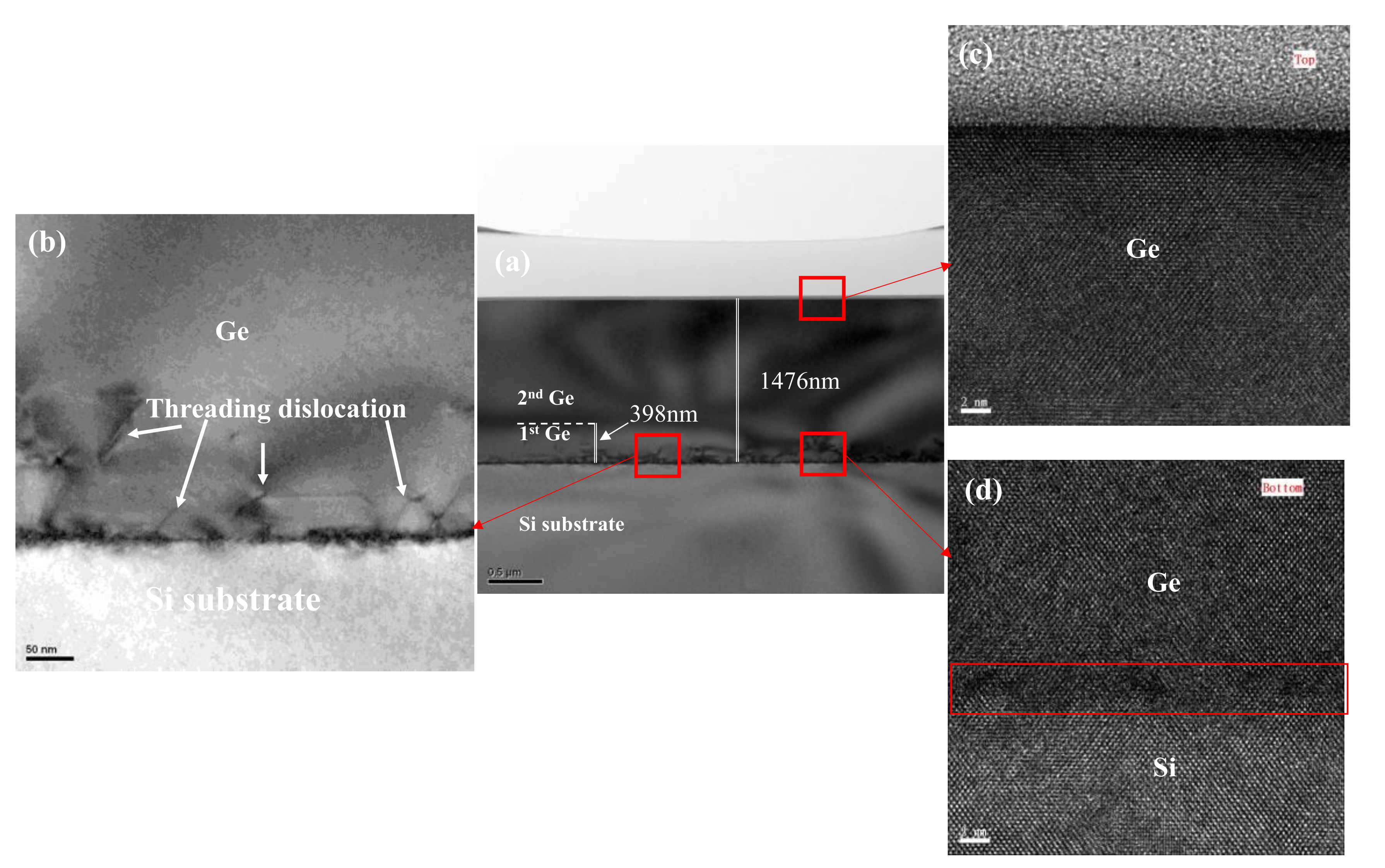
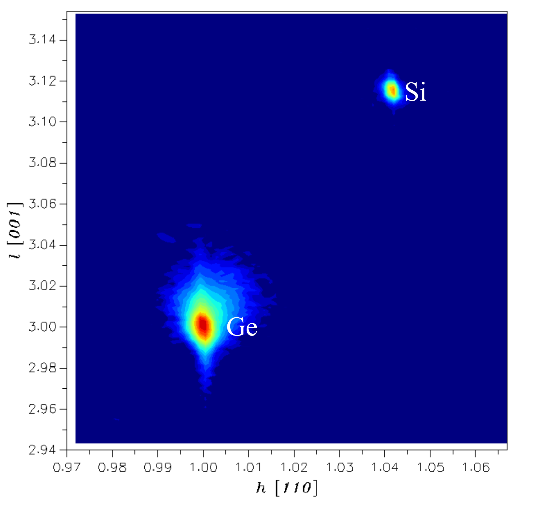
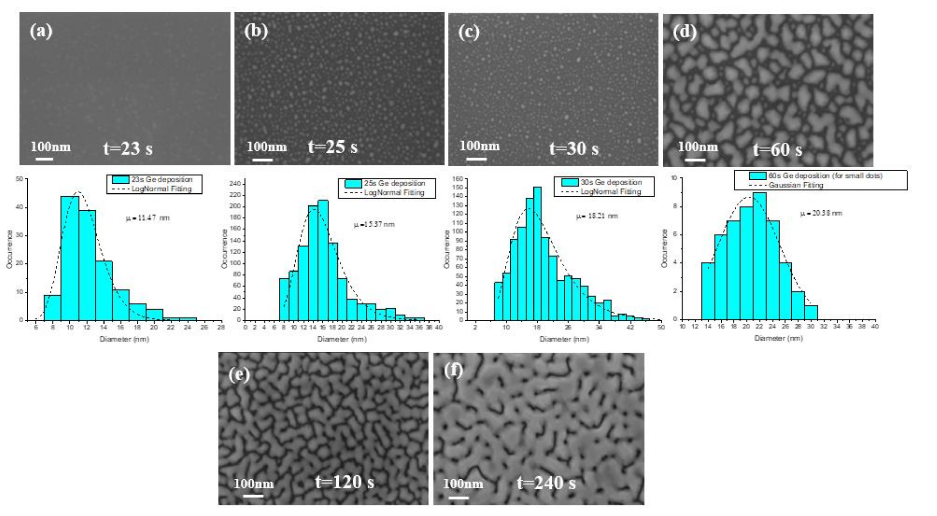
This work presents the growth of high-quality Ge epilayers on Si (001) substrates using a reduced pressure chemical vapor deposition (RPCVD) chamber. Based on the initial nucleation, a low temperature high temperature (LT-HT) two-step approach, we systematically investigate the nucleation time and surface topography, influence of a LT-Ge buffer layer thickness, a HT-Ge growth temperature, layer thickness, and high temperature thermal treatment on the morphological and crystalline quality of the Ge epilayers. It is also a unique study in the initial growth of Ge epitaxy; the start point of the experiments includes Stranski–Krastanov mode in which the Ge wet layer is initially formed and later the growth is developed to form nuclides. Afterwards, a two-dimensional Ge layer is formed from the coalescing of the nuclides. The evolution of the strain from the beginning stage of the growth up to the full Ge layer has been investigated. Material characterization results show that Ge epilayer with 400 nm LT-Ge buffer layer features at least the root mean square (RMS) value and it’s threading dislocation density (TDD) decreases by a factor of 2. In view of the 400 nm LT-Ge buffer layer, the 1000 nm Ge epilayer with HT-Ge growth temperature of 650 °C showed the best material quality, which is conducive to the merging of the crystals into a connected structure eventually forming a continuous and two-dimensional film. After increasing the thickness of Ge layer from 900 nm to 2000 nm, Ge surface roughness decreased first and then increased slowly (the RMS value for 1400 nm Ge layer was 0.81 nm). Finally, a high-temperature annealing process was carried out and high-quality Ge layer was obtained (TDD=2.78 × 107 cm−2). In addition, room temperature strong photoluminescence (PL) peak intensity and narrow full width at half maximum (11 meV) spectra further confirm the high crystalline quality of the Ge layer manufactured by this optimized process. This work highlights the inducing, increasing, and relaxing of the strain in the Ge buffer and the signature of the defect formation.
Keywords: Ge; optimization; parameter; threading dislocation; strain; RPCVD Ge; optimization; parameter; threading dislocation; strain; RPCVD