Article

Analysis of DC Characteristics in GaN-Based Metal-Insulator-Semiconductor High Electron Mobility Transistor with Variation of Gate Dielectric Layer Composition by Considering Self-Heating Effect

1
Division of Electronics and Electrical Engineering, Dongguk University-Seoul, Seoul 04620, Korea
2
Electronics and Telecommunications Research Institute, Daejeon 34129, Korea
3
Agency for Defense Development, Daejeon 34186, Korea
*
Author to whom correspondence should be addressed.
Appl. Sci. 2019, 9(17), 3610; https://doi.org/10.3390/app9173610
Submission received: 17 July 2019 / Revised: 27 August 2019 / Accepted: 30 August 2019 / Published: 2 September 2019
(This article belongs to the Special Issue NANO KOREA 2019)

Abstract

:
This study investigates metal-insulator-semiconductor high electron mobility transistor DC characteristics with different gate dielectric layer compositions and thicknesses, and lattice temperature effects on gate leakage current by using a two-dimensional simulation. We first compared electrical properties, including threshold voltage, transconductance, and gate leakage current with the self-heating effect, by applying a single Si3N4 dielectric layer. We then employed different Al2O3 dielectric layer thicknesses on top of the Si3N4, and also investigated lattice temperature across a two-dimensional electron gas channel layer with various dielectric layer compositions to verify the thermal effect on gate leakage current. Gate leakage current was significantly reduced as the dielectric layer was added, and further decreased for a 15-nm thick Al2O3 on a 5-nm Si3N4 structure. Although the gate leakage current increased as Al2O3 thickness increased to 35 nm, the breakdown voltage was improved.

1. Introduction

GaN-based high electron mobility transistors (HEMTs) have been studied as promising power devices for various applications, such as a communication base transceiver station and military radar equipment, due to their superior material characteristics, including high breakdown voltage, high electron mobility, high thermal conductivity, and wide bandgap [1,2,3]. However, a gate leakage current degrades a device’s electrical properties, power efficiency, and stability during operation. Generally, a gate leakage current is affected by a high lattice temperature and electric field and occurs mostly near the drain-side gate head edge [4,5,6,7,8,9,10]. When an insulator is placed between the gate metal and semiconductor, i.e., metal-insulator-semiconductor field-effect transistor, an electric field generated by the gate voltage is strongly formed in the insulator having a large resistance, such that the input impedance becomes very large and the gate leakage current can be reduced. Gate leakage current in GaN-based HEMTs can be reduced using structures similar to metal-insulator-semiconductor high electron mobility transistors (MIS-HEMTs), where high-k materials, such as Si3N4 and Al2O3, are deposited under the gate metal [11,12,13,14,15,16,17,18]. MIS-HEMTs have been studied by adding a high quality single dielectric layer, such as Si3N4, Al2O3, SiO2, HfO2, Sc2O3, GaO3, or ZrO2, to suppress current collapse, improve current flow, and reduce gate leakage current [14,15,16,17,19,20]. However, various dielectric layers deposited on top of a GaN-based HEMT cause an interface state trap and mechanical stresses, resulting in changes in threshold voltage and carrier concentration, respectively. Therefore, appropriate dielectric material and thickness selections are required. The Si3N4 dielectric layer causes compressive stress, but the Al2O3 dielectric layer deposited on the Si3N4 dielectric layer generates tensile stress. Since proper tensile stress helps to increase the carrier concentration compared to compressive stress, the combination of Si3N4 and Al2O3 layer thicknesses is very important [21].
This study investigated transfer I–V characteristics, gate leakage current, lattice temperature across two-dimensional electron gas (2-DEG) channel layer, and MIS-HEMT drain current variation by changing the dielectric layer compositions and thicknesses with the help of a two-dimensional simulator [22]. To begin with, we compared electrical properties, including threshold voltage, transconductance, and gate leakage current with the self-heating effect (SHE) by applying a single Si3N4 dielectric layer. We then employed different Al2O3 dielectric layer thicknesses on top of the Si3N4 and analyzed the lattice temperature across the 2-DEG channel layer to verify the thermal effect on the gate leakage current. Finally, we discuss an optimized MIS-HEMT structure as a normally-on device.

2. Materials and Methods

This study analyzed and compared MIS-HEMT transfer I–V characteristics for different dielectric layer compositions and thicknesses, as shown in Figure 1. Figure 1a,b shows schematic views of a basic AlGaN/GaN-based HEMT (BG-HEMT) and MIS-HEMT, respectively. Figure 1c represents the composition and thickness of distinct dielectric layers A, B, and C. Table 1 summarizes the BG-HEMT layer information, where the nominal Al composition of the AlGaN layer was 26%.
We used two gate leakage current models to compare the BG-HEMT and MIS-HEMT structures’ gate leakage currents. Figure 2a depicts the Poole–Frenkel thermal emission (PF) mechanism principle. Crystalline mismatches between layers when fabricating AlGaN/GaN HEMTs cause trap and continuum energy states in the barrier material. Electrons captured in trap energy states move to continuum energy states via high electric fields and temperatures, and current is generated by the voltage drop in the high reverse gate voltages. Figure 2b shows the Fowler–Nordheim tunneling (FN) mechanism. The barrier becomes thinner under high electric fields, allowing more electrons to penetrate the barrier and generate a current at high forward gate voltages [23,24,25]. The interface trap between the insulator and semiconductor is inevitable while growing epitaxial layers and causes the 2-DEG concentration and threshold voltage to become unstable. Therefore, it is essential to consider the interface trap density [26,27]. To obtain more accurate data, we set the interface trap density at the dielectric layer/GaN cap interface and acceptor trap density in the GaN buffer layer. Figure 3a shows the interface trap density at the Si3N4/GaN cap interface = 2.1 × 1012 cm−2, and Figure 3b shows acceptor trap density doping profile in GaN buffer layer = 2.09 × 1015 cm−3 at the unintentionally doped (UID) GaN/GaN buffer interface [28].
Since the thermal conductivity of the material affects the heat transfer during operation of the device and depends on the temperature, the lattice heat flow based on the thermal conductivity model is essential to considering SHE [29]. The thermal conductivity model is given by:
k T L = T C . C O N S T / T L 300 T C . N P O W
where T C . C O N S T , T L , and T C . N P O W are the thermal conductivity constant at 300 K, local lattice temperature, and coefficient of temperature dependence of thermal conductivity, respectively. As shown in Table 2, thermal conductivity constants of GaN and AlGaN were applied. Then, the lattice heat flow model is applied by using the calculated thermal conductivity, and it can be expressed as
C T L t =   k T L + H
where C , k , H , and T L are the heat capacitance per unit volume, thermal conductivity, heat generation, and local lattice temperature, respectively. k is calculated using Equation (1), and H is expressed as:
H = J n 2 q μ n n + J p 2 q μ p p T L J n P n T L J p P p + q R G T L φ n T n . p φ n φ p T n . p + φ p T L φ n T n . p + P n d i v J n T L φ p T n . p + P p d i v J p
In the steady-state, the current divergence can be replaced by the net recombination. Equation (3) then simplifies to:
H = J n 2 q μ n n + J p 2 q μ p p + q R G φ p φ n + T L P p P n T L ( J n P n + J p P p )
where J n 2 q μ n n + J p 2 q μ p p is the Joule heating effect term, q R G φ p φ n + T L P p P n is the heating and cooling term considering recombination and generation, and T L ( J n P n + J p P p ) accounts for the Peltier and Joule–Thomson effects. A simple and intuitive form of H that has been widely used in the past is:
H = ( J n + J p ) · E
where H is the generated heat, J n and J p are electron and hole current densities, respectively, and E is the electric field. SHE can be estimated using either Equation (4) or (5) for steady-state calculations. By default, Equation (5) is used.
We set the work function of the gate, source, and drain metals for Schottky and ohmic contacts, respectively. However, in the case of MIS-HEMT, the work function changes because of dielectric layers, even if the work function of the gate metal is fixed. This is due to the high-k effective work function model, which is expressed as:
Φ m e f f = E h i g h k + S h i g h k Φ m   E h i g h k
where Φ m e f f is the effective gate work function, E h i g h k is the high-k material charge neutrality, S h i g h k is a slope parameter of the high-k material, and Φ m is the metal work function in a vacuum ( Φ m = 3.73 eV for a Schottky contact [30]).
We considered auger recombination, Schockley–Read–Hall recombination, strain piezoelectric polarization, Selberherr’s impact ionization model, self-heating, thermal conductivity, the Fermi–Dirac distribution function, Poole–Frenkel thermal emission, the Fowler-Nordheim tunneling model, and the high-k effective work function model for the physical calculations [31,32,33,34]. Table 2 shows AlGaN and GaN material parameters.
Figure 4 shows the thermal conductivities of GaN, Al2O3, and Si3N4 as a function of temperature. As temperature increases above 400 K, the thermal conductivity of Al2O3 becomes lower than that for Si3N4.

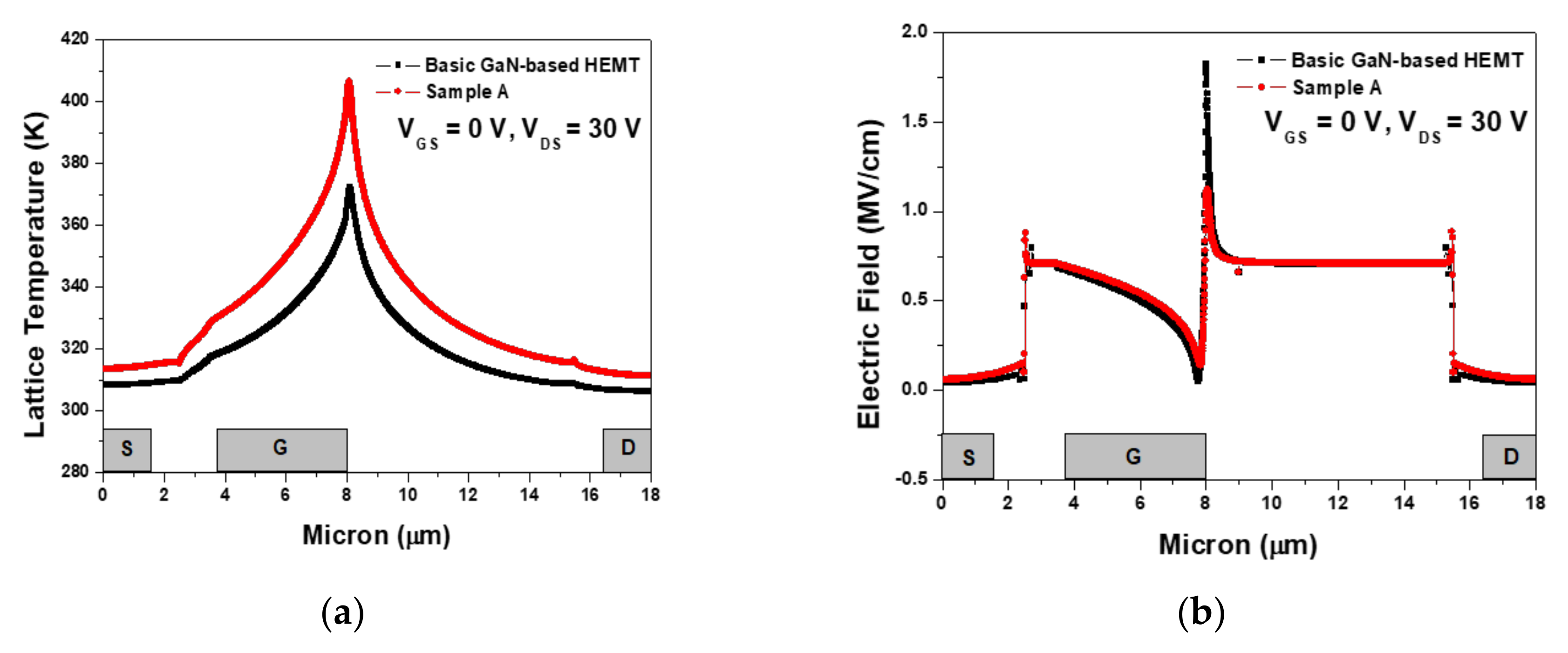
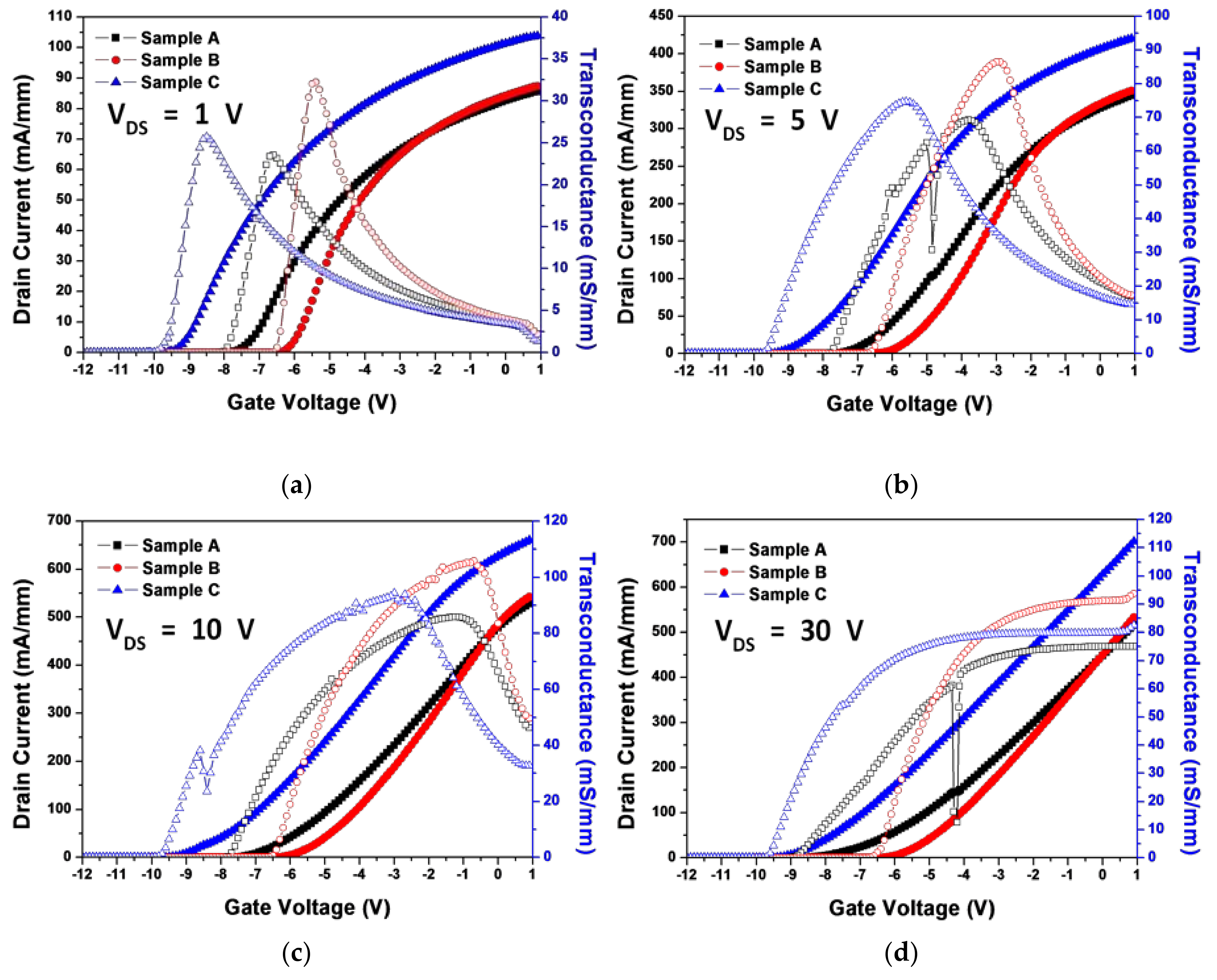
3. Results and Discussion

We first compared BG-HEMT and MIS-HEMT (sample A) transfer I–V characteristics for each drain voltage (VDS) = 1, 5, 10, and 30 V. The sample A threshold voltage shifted negatively to reach approximately −7.5 V, and the maximum transconductance decreased compared with BG-HEMT, as shown in Figure 5. The sample A drain current was generally larger than that for BG-HEMT and became much larger as VDS increased.
Figure 6 shows the measured gate leakage current with respect to the gate voltage (VGS) for VDS = 1, 5, 10, and 30 V. In the case of BG-HEMT, the gate leakage current decreased as VGS increased at low VDS = 1 and 5 V. However, at high VDS = 10 and 30 V, the gate leakage current decreased with increasing VGS, but increased again. The gate leakage current was affected by heat, and when VGS was above the threshold voltage of about −3.7 V, the gate leakage current increased because heat was generated by the device operation. In contrast, the gate leakage current was significantly reduced in sample A.
Figure 7 shows the lattice temperature and electric field across the 2-DEG channel layer of the BG-HEMT and sample A at VGS = 0 V and VDS = 30 V. Sample A’s lattice temperature in the 2-DEG channel layer was significantly higher than that for BG-HEMT, but sample A’s electric field was lower than that for BG-HEMT. Since the increase of current density was larger (see Figure 5d) than the decrease of the electric field in sample A, as shown in Figure 7b, the overall lattice temperature of sample A across the 2-DEG channel layer was larger than that of BG-HEMT, as shown in Figure 7a (see Equation (5)). Although the gate leakage current can be affected by temperature, the dielectric layer effectively reduced the gate leakage current [21].
After confirming that sample A’s gate leakage current was markedly reduced, the dielectric layer composition was changed, as shown in Figure 1c. We then compared the transfer I–V characteristics for these structures when VDS = 1, 5, 10, and 30 V. Figure 8 shows the threshold voltages, maximum transconductances, and drain currents for samples A, B, and C. Sample B’s threshold voltage shifted toward the positive direction as compared with sample A, and sample C shifted toward the negative direction [35]. Sample B and C’s threshold voltages were about −6.2 and −9.4 V, respectively. Maximum transconductance was achieved for sample B, then C and A, in descending order. However, the drain current exhibited different tendencies, with sample C obtaining the highest value, then sample B and A, in descending order.
Samples A, B, and C’s gate leakage currents were simulated at high VDS = 10 and 30 V. Figure 9 shows that sample B’s gate leakage current was significantly reduced compared with sample A, even though the values were extremely low. Since the actual physical phenomena occurring in the device were not known, the results only represented the tendency of the gate leakage current depending on the dielectric layer composition and thickness. Sample C’s gate leakage current exceeded sample B’s. Thus, Al2O3 deposition on Si3N4 effectively reduced the gate leakage current, but the gate leakage current increased with thicker Al2O3 on Si3N4.
Figure 10a shows that sample C’s lattice temperature across the 2-DEG channel layer was the highest, with samples A and B exhibiting similar values when VGS = 0 V and VDS = 30 V. The highest peaks occurred at the drain-side gate head edges with 441.94, 406.64, and 406.38 K for samples C, A, and B, respectively. However, the electric field distributions for the three structures were different. Sample A was the highest, followed by samples B and C at the drain-side gate head edge. As shown in Figure 5; Figure 7, sample C’s lattice temperature across the 2-DEG channel layer was higher than sample B because sample C’s effective current density was also higher, as shown in Figure 8. Figure 10b shows that sample C exhibited an even lower electric field at the drain-side gate edge, which resulted in an increasing gate leakage current, as shown in Figure 9. As the thickness of the insulator increased, the current due to the tunneling effect decreased. However, when the thickness of the insulator increased, the threshold voltage, stress, and heat transfer must be considered. In the case of samples B and C, the dielectric layer composition was a combination of Al2O3 and Si3N4. Since the barrier height in samples B and C were larger than for A, the gate leakage current by FN tunneling was reduced. For sample C, the electric field was the lowest, but the current density was the highest at VGS = 0 V and VDS = 30 V, resulting in generating more heat. In addition, the thermal conductivity of the materials must be taken into account in the heat transfer. The thermal conductivity of Al2O3 was lower than that of Si3N4. The induced heat confined in the Al2O3 further lowered the barrier height and increased the gate leakage current.
Figure 11 shows the MIS-HEMT breakdown voltage characteristics. Depositing the Al2O3 on the Si3N4 dielectric layer improved the breakdown voltage. We set the breakdown voltage for the drain current = 1 mA/mm as a reference, and achieved breakdown voltage values that were about 94, 194, and 300 V at pinch-off voltages = −14, −12, and −12.6 V, respectively, considering each threshold voltage. Although the gate leakage current in sample C was larger than for sample B, it showed higher breakdown characteristics.
Figure 12 shows the MIS-HEMT saturation current characteristics with and without SHE for VGS = −2 to 0 V. SHE decreased the drain current for all three structures and made the current unstable. Sample C was more affected by SHE and sample B was less affected. Table 3 shows the calculated level of drain current degradation for all three structures. Although sample C had a higher breakdown voltage and drain current, the gate leakage current was higher and the drain current was more affected by SHE. Therefore, an appropriate Al2O3 thickness on Si3N4 is crucial to operating an AlGaN/GaN HEMT as a normally-on device.

4. Conclusions

This study provides a simulation study of transfer I–V characteristics, gate leakage current, and saturation current characteristics for MIS-HEMT structures by considering SHE. The gate leakage current increased with increasing temperature, but the MIS-HEMT gate leakage current was significantly lower than the basic AlGaN/GaN-based HEMT, even when temperature was increased by applying the gate dielectric layer. The gate dielectric layer, consisting of Si3N4 and Al2O3, reduced the gate leakage current more than a single Si3N4 gate dielectric layer did. However, the threshold voltage, gate leakage current, and breakdown voltage all changed depending on the dielectric layer composition and thickness. The MIS-HEMT gate leakage current and breakdown voltage with Al2O3 on Si3N4 were significantly improved compared with the device incorporating only Si3N4. However, the saturation current characteristics became too unstable to operate as a normally-on device for thicker Al2O3 layers. Future work will study MIS-HEMT structures in more detail, with wider ranges of dielectric layer compositions and thicknesses.

Author Contributions

Experiments and simulations, I.-T.H., K.-W.J., and H.-J.K.; fabrication, S.-H.L. and J.-W.L.; formal analysis, J.-M.Y. and H.-S.K. (Ho-Sang Kwon); supervision, H.-S.K. (Hyun-Seok Kim).

Funding

This work was supported by the program of Defense Acquisition Program Administration and Agency for Defense Development.

Conflicts of Interest

The authors declare no competing financial interests.

References

  1. Mishra, U.K.; Parikh, P.; Wu, Y.F. AlGaN/GaN HEMTs-an overview of device operation and applications. Proc. IEEE 2002, 90, 1022–1031. [Google Scholar] [CrossRef]
  2. Mishra, U.K.; Shen, L.; Kazior, T.E.; Wu, Y.F. GaN-based RF power devices and amplifiers. Proc. IEEE 2008, 96, 287–305. [Google Scholar] [CrossRef]
  3. Ambacher, O.; Foutz, B.; Smart, J.; Shealy, J.R.; Weimann, N.G.; Chu, K.; Murphy, M.; Sierakowski, A.J.; Schaff, W.J.; Eastman, L.F.; et al. Two dimensional electron gases induced by spontaneous and piezoelectric polarization in undoped and doped AlGaN/GaN heterostructures. J. Appl. Phys. 2000, 87, 334–344. [Google Scholar] [CrossRef]
  4. Chung, J.W.; Roberts, J.C.; Piner, E.L.; Palacios, T. Effect of gate leakage in the subthreshold characteristics of AlGaN/GaN HEMTs. IEEE Electron Device Lett. 2008, 29, 1196–1198. [Google Scholar] [CrossRef]
  5. Kim, H.; Lee, J.; Liu, D.; Lu, W. Gate current leakage and breakdown mechanism in unpassivated AlGaN/GaN high electron mobility transistors by post-gate annealing. Appl. Phys. Lett. 2005, 86, 143505. [Google Scholar] [CrossRef]
  6. Park, Y.J.; Kwak, H.T.; Chang, S.B.; Kim, H.S. Breakdown Voltage Enhancement in AlGaN/GaN High-Electron Mobility Transistor by Optimizing Gate Field-Plate Structure. J. Nanosci. Nanotechnol. 2019, 19, 2298–2301. [Google Scholar] [CrossRef] [PubMed]
  7. Arulkumaran, S.; Egawa, T.; Ishikawa, H.; Jimbo, T. Temperature dependence of gate–leakage current in AlGaN/GaN high-electron-mobility transistors. Appl. Phys. Lett. 2003, 82, 3110–3112. [Google Scholar] [CrossRef]
  8. Yan, D.; Lu, H.; Cao, D.; Chen, D.; Zhang, R.; Zheng, Y. On the reverse gate leakage current of AlGaN/GaN high electron mobility transistors. Appl. Phys. Lett. 2010, 97, 153503. [Google Scholar] [CrossRef]
  9. Wang, A.; Zeng, L.; Wang, W. Simulation of Gate Leakage Current of AlGaN/GaN HEMTs: Effects of the Gate Edges and Self-Heating. ECS J. Solid State Sci. Technol. 2017, 6, 3025–3029. [Google Scholar] [CrossRef]
  10. Kwak, H.T.; Chang, S.B.; Kim, H.J.; Jang, K.W.; Yoon, H.; Lee, S.H.; Lim, J.W.; Kim, H.S. Operational Improvement of AlGaN/GaN High Electron Mobility Transistor by an Inner Field-Plate Structure. Appl. Sci. 2018, 8, 974. [Google Scholar] [CrossRef]
  11. Ye, G.; Wang, H.; Arulkumaran, S.; Ng, G.I.; Hofstetter, R.; Li, Y.; Anand, M.J.; Ang, K.S.; Maung, Y.K.Y.; Foo, S.C. Atomic layer deposition of ZrO2 as gate dielectrics for AlGaN/GaN metal-insulator-semiconductor high electron mobility transistors on silicon. Appl. Phys. Lett. 2013, 103, 142109. [Google Scholar] [CrossRef]
  12. Zhu, J.J.; Ma, X.H.; Xie, Y.; Hou, B.; Chen, W.W.; Zhang, J.C.; Hao, Y. Improved interface and transport properties of AlGaN/GaN MIS-HEMTs with PEALD-grown AlN gate dielectric. IEEE Trans. Electron Devices 2014, 62, 512–518. [Google Scholar]
  13. Chou, P.C.; Chen, S.H.; Hsieh, T.E.; Cheng, S.; Del Alamo, J.; Chang, E. Evaluation and reliability assessment of GaN-on-Si MIS-HEMT for power switching applications. Energies 2017, 10, 233. [Google Scholar] [CrossRef]
  14. Yue, Y.-Z.; Hao, Y.; Feng, Q.; Zhang, J.-C.; Ma, X.-H.; Ni, J.-Y. GaN MOS-HEMT using ultra-thin Al2O3 dielectric grown by atomic layer deposition. Chin. Phys. Lett. 2007, 24, 2419. [Google Scholar]
  15. Liu, C.; Chor, E.F.; Tan, L.S. Enhanced device performance of AlGaN/GaN HEMTs using HfO2 high-k dielectric for surface passivation and gate oxide. Semicond. Sci. Technol. 2007, 22, 522. [Google Scholar] [CrossRef]
  16. Pérez-Tomás, A.; Fontserè, A.; Jennings, M.R.; Gammon, P.M. Modeling the effect of thin gate insulators (SiO2, SiN, Al2O3 and HfO2) on AlGaN/GaN HEMT forward characteristics grown on Si, sapphire and SiC. Mater. Sci. Semicond. Process. 2013, 16, 1336–1345. [Google Scholar] [CrossRef]
  17. Lu, X.; Ma, J.; Jiang, H.; Liu, C.; Xu, P.; Lau, K.M. Fabrication and Characterization of Gate-Last Self-Aligned AlN/GaN MISHEMTs WithIn SituSiN x Gate Dielectric. IEEE Trans. Electron Devices 2015, 62, 1862–1869. [Google Scholar]
  18. Kwak, H.T.; Chang, S.B.; Jung, H.G.; Kim, H.S. Thermal analysis of AlGaN/GaN high-electron-mobility transistor and its RF power efficiency optimization with source-bridged field-plate structure. J. Nanosci. Nanotechnol. 2018, 18, 5860–5867. [Google Scholar] [CrossRef]
  19. Hashizume, T.; Nishiguchi, K.; Kaneki, S.; Kuzmik, J.; Yatabe, Z. State of the art on gate insulation and surface passivation for GaN-based power HEMTs. Mater. Sci. Semicond. Process. 2018, 78, 85–95. [Google Scholar] [CrossRef]
  20. Lu, X.; Yu, K.; Jiang, H.; Zhang, A.; Lau, K.M. Study of interface traps in AlGaN/GaN MISHEMTs using LPCVD SiN x as gate dielectric. IEEE Trans. Electron Devices 2017, 64, 824–831. [Google Scholar] [CrossRef]
  21. Chang, S.J.; Jung, H.W.; Do, J.W.; Cho, K.J.; Kim, J.J.; Jang, Y.J.; Yoon, H.S.; Ahn, H.K.; Min, B.G.; Kim, H.; et al. Enhanced Carrier Transport Properties in GaN-Based Metal-Insulator-Semiconductor High Electron Mobility Transistor with SiN/Al2O3 Bi-Layer Passivation. ECS J. Solid State Sci. Technol. 2018, 7, N86–N90. [Google Scholar] [CrossRef]
  22. Silvaco, Inc. Silvaco Atlas, ver. 5.22.1.R, Semiconductor Device Modeling System. Available online: https://www.silvaco.com/products/tcad/device_simulation/atlas/atlas.html (accessed on 2 September 2019).
  23. Turuvekere, S.; Karumuri, N.; Rahman, A.A.; Bhattacharya, A.; DasGupta, A.; DasGupta, N. Gate leakage mechanisms in AlGaN/GaN and AlInN/GaN HEMTs: Comparison and modeling. IEEE Trans. Electron Devices 2013, 60, 3157–3165. [Google Scholar] [CrossRef]
  24. Dutta, G.; DasGupta, N.; DasGupta, A. Gate leakage mechanisms in AlInN/GaN and AlGaN/GaN MIS-HEMTs and its modeling. IEEE Trans. Electron Devices 2017, 64, 3609–3615. [Google Scholar] [CrossRef]
  25. Mitrofanov, O.; Manfra, M. Poole-Frenkel electron emission from the traps in AlGaN/GaN transistors. J. Appl. Phys. 2004, 95, 6414–6419. [Google Scholar] [CrossRef] [Green Version]
  26. Longobardi, G.; Udrea, F.; Sque, S.; Hurkx, G.A.; Croon, J.; Napoli, E.; Šonský, J. Impact of donor traps on the 2DEG and electrical behavior of AlGaN/GaN MISFETs. IEEE Electron Device Lett. 2014, 35, 27–29. [Google Scholar] [CrossRef]
  27. Mehari, S.; Gavrilov, A.; Eizenberg, M.; Ritter, D. Density of traps at the insulator/III-N interface of GaN heterostructure field-effect transistors obtained by gated Hall measurements. IEEE Electron Device Lett. 2015, 36, 893–895. [Google Scholar] [CrossRef]
  28. Kwak, H.T.; Jang, K.W.; Kim, H.J.; Lee, S.H.; Lim, J.W.; Kim, H.S. DC Characteristics of AlGaN/GaN High-Electron Mobility Transistor with a Bottom Plate Connected to Source-Bridged Field Plate Structure. J. Nanosci. Nanotechnol. 2019, 19, 2319–2322. [Google Scholar] [CrossRef]
  29. Vitanov, S.; Palankovski, V.; Maroldt, S.; Quay, R. High-temperature modeling of AlGaN/GaN HEMTs. Solid-State Electron. 2010, 54, 1105–1112. [Google Scholar] [CrossRef]
  30. Yeo, Y.C.; King, T.J.; Hu, C. Metal-dielectric band alignment and its implications for metal gate complementary metal-oxide-semiconductor technology. J. Appl. Phys. 2002, 92, 7266–7271. [Google Scholar] [CrossRef] [Green Version]
  31. Chuang, S.L. Optical gain of strained wurtzite GaN quantum-well lasers. IEEE J. Quantum Electron. 1996, 32, 1791–1800. [Google Scholar] [CrossRef]
  32. Kuzmík, J. InAlN/(In) GaN high electron mobility transistors: Some aspects of the quantum well heterostructure proposal. Semicond. Sci. Technol. 2002, 17, 540. [Google Scholar] [CrossRef]
  33. Chvála, A.; Nagy, L.; Marek, J.; Priesol, J.; Donoval, D.; Blaho, M.; Gregušová, D.; Kuzmík, J.; Šatka, A. Characterization of monolithic InAlN/GaN NAND logic cell supported by circuit and device simulations. IEEE Trans. Electron Devices 2018, 65, 2666–2669. [Google Scholar] [CrossRef]
  34. Selberherr, S. MOS device modeling at 77 K. IEEE Trans. Electron Devices 1989, 36, 1464–1474. [Google Scholar] [CrossRef]
  35. Dutta, G.; Turuvekere, S.; Karumuri, N.; DasGupta, N.; DasGupta, A. Positive shift in threshold voltage for reactive-ion-sputtered Al2O3/AlInN/GaN MIS-HEMT. IEEE Electron Device Lett. 2014, 35, 1085–1087. [Google Scholar] [CrossRef]
Figure 1. Basic AlGaN/GaN-based MIS-HEMT (a) without and (b) with a dielectric layer, and (c) dielectric layer composition and thickness for samples A, B, and C.
Applsci 09 03610 g001
Figure 2. Mechanism of gate leakage current models: (a) Poole–Frenkel thermal emission, and (b) Fowler–Nordheim tunneling.
Applsci 09 03610 g002
Figure 3. (a) Interface trap density at the Si3N4/GaN cap interface, and (b) GaN buffer layer acceptor trap density doping profile with respect to depth.
Applsci 09 03610 g003
Figure 4. Thermal conductivities for GaN, Al2O3, and Si3N4 with respect to temperature.
Applsci 09 03610 g004
Figure 5. Transfer I–V characteristics for BG-HEMT and MIS-HEMT (sample A) at (a) VDS = 1 V, (b) VDS = 5 V, (c) VDS = 10 V, and (d) VDS = 30 V (drain current (filled dot), transconductance (empty dot)).
Applsci 09 03610 g005
Figure 6. Gate leakage current for BG-HEMT and MIS-HEMT (sample A) with respect to VGS at (a) VDS = 1 V, (b) VDS = 5 V, (c) VDS = 10 V, and (d) VDS = 30 V.
Applsci 09 03610 g006
Figure 7. (a) Lattice temperature, and (b) electric field distributions across the 2-DEG channel layer with and without the Si3N4 dielectric layer at VGS = 0 V and VDS = 30 V.
Applsci 09 03610 g007
Figure 8. Comparison of transfer I–V characteristics of MIS-HEMTs (samples A, B, and C) with respect to VGS at (a) VDS = 1 V, (b) VDS = 5 V, (c) VDS = 10 V, and (d) VDS = 30 V (drain current (filled dot), transconductance (empty dot)).
Applsci 09 03610 g008
Figure 9. Gate leakage current for MIS-HEMTs (samples A, B, and C) with respect to VGS at (a) VDS = 10 V and (b) VDS = 30 V.
Applsci 09 03610 g009
Figure 10. (a) Lattice temperature, and (b) electric field distributions across 2-DEG channel layer for MIS-HEMTs (samples A, B, and C) at VGS = 0 V, and VDS = 30 V.
Applsci 09 03610 g010
Figure 11. Breakdown voltage characteristics for MIS-HEMTs (samples A, B, and C).
Applsci 09 03610 g011
Figure 12. Saturation current characteristics for MIS-HEMT with and without the self-heating effect (SHE) as a normally-on device: (a) sample A, (b) sample B, and (c) sample C.
Applsci 09 03610 g012aApplsci 09 03610 g012b
Table 1. Basic AlGaN/GaN-based HEMT geometrical parameters.
ParameterValue
L S G 1.0 µm
L G 4.5 µm
L G D 9.5 µm
GaN Cap2.0 nm
AlGaN 21 nm
AlN1.0 nm
UID GaN Channel0.1 µm
GaN Buffer1.8 µm
Table 2. Material parameters used for simulations at temperature 300 K.
ParameterGaNAlGaN
Bandgap energy (eV)3.393.89
Electron affinity (eV)43.6
Low field mobility (cm2 V−1 s−1)990300
Relative permittivity9.59.38
Thermal conductivity constant (W cm−1 K−1)1.30.4
TC.NPOW0.43-
High field mobility modelGANSAT saturation velocity model
Electron Saturation velocity (cm s-1)1.9 × 1071.12 × 107
Table 3. Drain current variation due to the self-heating effect.
TypeΔID (mA/mm) (at VDS = 40 V)
VGS = −2.0 VVGS = −1.5 VVGS = −1.0 VVGS = −0.5 VVGS = 0.0 V
A−45.17−58.38−73.23−89.49−107.41
B−44.49−60.10−77.99−98.01−119.92
C−138.17−161.87−187.07−213.58−241.27

