Abstract
This paper presents a CMOS wideband amplifier operating in the full Ka-band, with a low gain variation. An inductive neutralization is applied to the amplifier to compensate for the gain roll-off in the high-frequency region. Neutralization inductance is carefully determined considering the tradeoff between stability and gain. To achieve a low gain variation over the full Ka-band, the amplifier employs the frequency staggering technique in which impedance matching for three gain stages is performed at different frequencies of 26, 34, and 42 GHz. The experimental results show that a peak gain of 13.2 dB is achieved at 39.2 GHz. The 3 dB bandwidth is from 23.5 to 41.7 GHz, which fully covers the Ka-band. Especially, the gain ripple of the amplifier is only 13 ± 0.2 dB over a wide bandwidth from 26.2 to 40.2 GHz. The input and output return loss values are better than −10 dB from 26.3 to 40.1 GHz and from 25.3 to 50 GHz, respectively. The DC power consumption is 18.6 mW.
1. Introduction
Owing to the demand for high-speed data transfer, 5G communication based on the millimeter wave has been actively developed. The global spectrum allocated for the 5G millimeter wave is mainly distributed in the Ka-band (26.5–40 GHz) [1,2]. Therefore, a wideband flat-gain amplifier operating in the full Ka-band is needed for implementing multistandard or ultrawideband radio systems supporting the global spectrum.
Conventionally, wideband amplifiers operating at several gigahertz have been implemented using a resistive feedback technique [3,4,5]. The resistive feedback makes the input impedance more resistive, thereby allowing wideband input matching and enhancing the linearity [6]. However, a disadvantage of the resistive feedback is that the gain decreases in the upper end of the bandwidth [7]. Therefore, multiple amplifying stages must be cascaded to compensate for the gain roll-off, which increases the overall DC power consumption. Recently, a feedback technique based on a transformer balun was proposed to achieve a wideband gain response with a compact size [8,9]. However, the complicated structure of the transformer balun makes it challenging to optimize the transformer parameters such as the primary and secondary inductances and the coupling coefficient to achieve both the wideband input matching and flat-gain response at the same time.
This paper presents a full Ka-band amplifier with a low gain variation. In the first gain stage, the inductive neutralization is adopted to compensate for the gain roll-off in the upper end of the Ka-band, while the frequency staggering is employed in the subsequent gain stages for wideband and flat-gain responses. In Section 2, the analysis and design of the amplifier are presented. The experimental results are presented in Section 3. Finally, the conclusions are drawn in Section 4.
2. Circuit Analysis and Design
Figure 1 shows a schematic of the full Ka-band flat-gain CMOS amplifier using the inductive neutralization and frequency staggering techniques. Three common-source (CS) gain stages (M1, M2, and M3) were cascaded to secure a sufficient gain. To accomplish a wideband flat-gain response over the full Ka-band, the inductive neutralization was applied to the first stage, while the frequency staggering was employed in the following interstage and output matching networks.
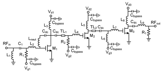
Figure 1.
Schematic of the full Ka-band amplifier with flat gain.
2.1. Inductive Neutralization Technique
To achieve a high flat gain, the optimum transistor topology was determined first. Figure 2 shows the maximum stable gain (MSG) (or the maximum available gain (MAG)) [10] of various transistor topologies in the given 65 nm CMOS technology.
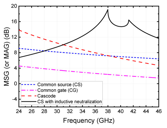
Figure 2.
Comparison of MSG (or MAG) of different transistor topologies in a 65 nm CMOS technology.
For a fair comparison, the simulation conditions were set identical: the gate width and drain bias current of each transistor are 30 μm and 3.1 mA, respectively. Among the CS, common-gate (CG), and cascade topologies, the CS topology provides the highest gain beyond 38 GHz. However, the gain of the CS still gradually decreases as the frequency increases further than 38 GHz. To achieve a flat gain over the full Ka-band, a gain-boosting technique should be used to compensate for the gain roll-off at the upper end of the Ka-band.
In this research, we adopted the inductive neutralization technique in the CS to boost the gain. It is well known that the gate-drain capacitance Cgd degrades the forward gain of the transistor [11]. Therefore, by connecting a neutralization inductor (Lneut) between the gate and drain, Cgd is resonated with the inductor, and thus the MSG (or MAG) can be boosted [12,13]. In Figure 2, the MSG (or MAG) of the CS topology with the inductive neutralization (Lneut = 1.3 nH) is shown, which is higher than that of other topologies beyond 31 GHz. Moreover, the inductive neutralization changes the behavior of the MSG (or MAG) over the frequency. It is observed in Figure 2 that the peak of the MSG (or MAG) is pushed to a higher frequency region and, thus, can be located almost at the upper end of the Ka-band. This offsets the high loss of passive matching components and the resulting gain roll-off at the high frequencies.
While boosting the gain by resonating out the feedback capacitance Cgd, the inductive neutralization may disrupt the stability of the transistor. This is because positive feedback can be reinforced when the Cgd–Lneut network operates far from the resonance. Therefore, the value of Lneut should be carefully determined considering a tradeoff between the gain and the stability. Figure 3 shows the simulated MSG (or MAG) and stability factor K at 39 GHz versus Lneut. The MSG (or MAG) has two peaks at Lneut = 1.23 and 1.44 nH, respectively. On the other hand, the K has a single peak at Lneut = 1.3 nH and decreases rapidly as Lneut deviates from 1.3 nH. The K becomes even below unity when Lneut < 1.23 nH or Lneut > 1.44 nH. Hence, we chose Lneut of 1.3 nH, which results in MAG of 15.1 dB and K of 11.2 at 39 GHz. Notably, both MAG and K are boosted by inductive neutralization. The inductive neutralization with Lneut of 1.3 nH was applied to the first gain stage (M1), which presents a high gain at the upper end of the Ka-band. It should be noted that the second and third gain stages (M2 and M3) have no inductive neutralization because they should present a high gain at lower frequencies, as described in Section 2.2.
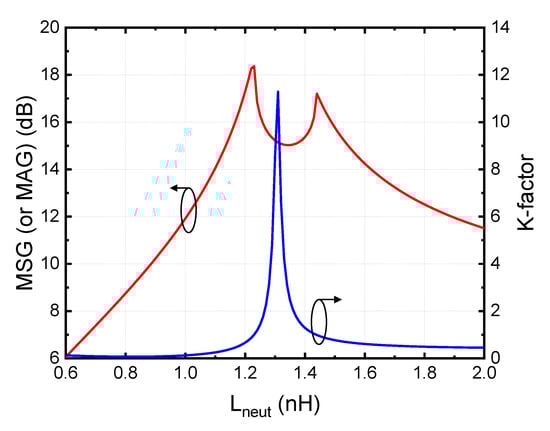
Figure 3.
Simulated MSG (or MAG) and stability factor K at 39 GHz versus Lneut.
The input matching of the amplifier should operate in a wide bandwidth to suppress mismatch loss that occurs in the interconnection with other circuit blocks. The inductive neutralization of the first gain stage alters the input impedance of M1; therefore, it should be considered in the input matching design shown in Figure 4. Specifically, the Cgd–Lneut network brings the load impedance of M1 (ZL1) to the input of M1 (Zin1) when the operation is off the resonance frequency. ZL1 includes the drain bias network of M1 (L3 and Cbypass), the input impedance looking into M2, and the interstage matching between M1 and M2. In Figure 5, the impedances of the input matching network are shown as the frequency is swept from 26 to 40 GHz. The Zin1 with no ZL1 and Lneut included is dominantly determined by the gate capacitance and resistance, as expected, shown in line (a). However, Zin1 with ZL1 included, shown in line (b), and with both ZL1 and Lneut included, shown in line (c), are substantially different from line (a). Fortunately, Lnuet induces a resonance behavior in Zin1, thereby providing a wideband characteristic to the input reflection coefficient. Finally, the input impedance at the port (Zin) is matched to 50 Ω with L1, C1, and L2, shown in line (d).
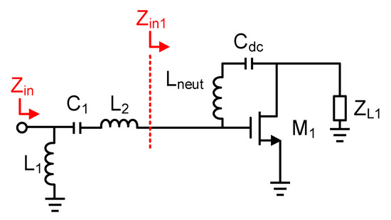
Figure 4.
Input matching network of the first gain stage.
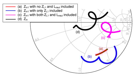
Figure 5.
Loci of the input impedances from 26 to 40 GHz.
2.2. Frequency Staggering Technique
To achieve a flat gain over a wide frequency range, the center frequencies of three gain stages (M1, M2, and M3) are intentionally staggered. Through the interstage and output impedance matching described below, the peak-gain frequencies of the first, second, and third stages are tuned to 42, 25.5, and 30.5 GHz, respectively, as shown in Figure 6.
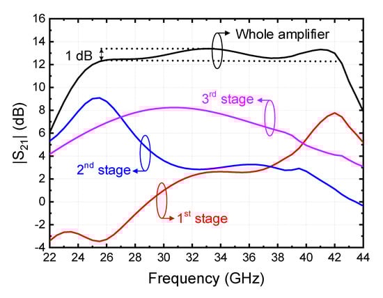
Figure 6.
Gain of the three individual stages and the whole amplifier.
The ac equivalent circuit of the amplifier is drawn in Figure 7a. For the first interstage matching between M1 and M2, the impedances seen looking into the output of M1 (Zout1) and the input of M2 (Zin2) are simulated as Zout1 = 48.3 − j89.2 Ω and Zin2 = 14.2 − j71.9 Ω at 42 GHz. For conjugate matching, Zin2 is transformed to Zout1* by an L-section network consisting of L3, L4, and TL1. As shown in Figure 7b, the series inductive components (L4 and TL1) bring Zin2 to Zin2,1, which is located on a constant conductance circle of Re{1/Zout1*}. Then, a shunt inductor (L3) transforms Zin2,1 to Zin2,2, which completes the conjugate matching to Zout1*. It should be noted that the value of L3 determines the frequency at which the conjugate matching is satisfied. In Figure 7b, the locus of Zin2,2 at 42 GHz is depicted as L3 decreases from infinity to 0.1 nH. According to the plot, L3 is chosen as 0.8 nH to achieve conjugate matching at 42 GHz. The final matching point of Zin2,2 slightly deviates from Zout1* after fine optimization of the whole amplifier. The conjugate interstage matching between M1 and M2 at 42 GHz results in the gain peak of the first gain stage at the same frequency as that shown in Figure 6.
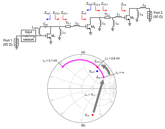
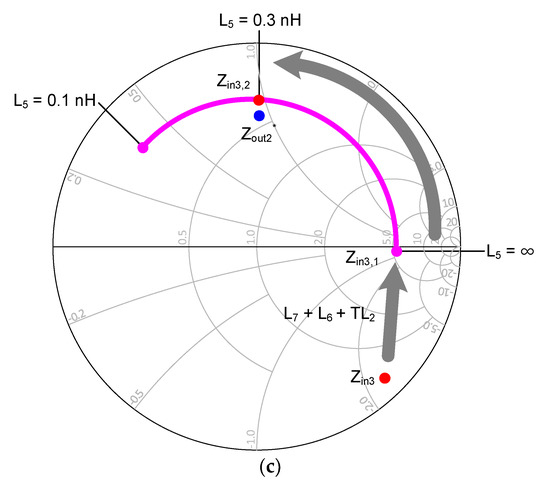
Figure 7.
Interstage matching: (a) AC equivalent circuit of the amplifier; (b) first interstage matching at 42 GHz; (c) second interstage matching at 26 GHz.
The second interstage matching between M2 and M3 is performed in a similar way to the first interstage matching. However, the matching frequency is intentionally changed to 26 GHz. As shown in Figure 7c, the input impedance of M3 (Zin3) is transformed to the conjugate of the output impedance of M2 (Zout2*). The center frequency of the matching is tuned to 26 GHz by choosing the value of a shunt inductor (L5) as 0.3 nH. It is noted that the second interstage matching is supposed to have the matching performance sensitive to the adjacent stages more than the first interstage matching. This is because the adjacent impedances are seen through Cgd of M2 and M3, while Cgd of M1 is diminished by the neutralization inductor Lneut. Therefore, an extra shunt inductor (L6) is added as an additional degree of design freedom in the second interstage matching while minimizing the influence on the adjacent matching. The second interstage matching results in the gain peak of the second stage at 25.5 GHz, as observed in Figure 6.
The output matching is fulfilled by L8 and L9 at 34 GHz, which leads to the peak gain of the final stage at 30.5 GHz shown in Figure 6. It is noted that there is a slight difference between the matching frequency and the peak gain frequency of each individual stage. This is because the gain and bandwidth of the whole amplifier were re-optimized after combining the individual stages.
Through the frequency staggering, the overall gain of the whole amplifier exhibits a flat response of 12.8 ± 0.5 dB from 25.6 to 42.4 GHz, covering the full Ka-band, as shown in Figure 6. After full electromagnetic simulation with Keysight ADS Momentum, the values of the matching components are slightly reoptimized considering the undesired magnetic and electric coupling between matching components and interconnection lines. The design parameter values of the full Ka-band amplifier are listed in Table 1.

Table 1.
Design parameter values of the full Ka-band amplifier.
3. Experimental Results
The full Ka-band amplifier was fabricated using a 65 nm CMOS technology. The chip micrograph is shown in Figure 8. The whole chip area including the probing pads and the core chip area were 1 × 0.7 and 0.5 × 0.75 , respectively.
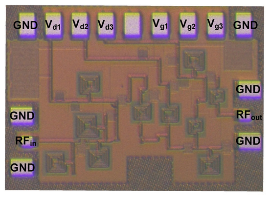
Figure 8.
Chip micrograph of the full Ka-band amplifier.
The measured S-parameters are shown in Figure 9. A peak gain of 13.2 dB was measured at 39.2 GHz. The 3 dB bandwidth was 18.2 GHz from 23.5 to 41.7 GHz, which covered the entire Ka-band frequencies. Specifically, from 26.2 to 40.2 GHz, the gain exhibited a flat response with a small variation, i.e., 13 ± 0.2 dB. The measured |S11| and |S22| were smaller than −10 dB from 26.3 to 40.1 GHz. The stability K-factor was calculated from the measured S-parameters, as shown in Figure 10. It was observed that the Ka-band amplifier was stable over the frequencies from DC to 50 GHz, which include both the operation and the out-of-band frequencies. The measured group delay is shown in Figure 11. The group delay was fairly flat in the frequency range between 22 and 46 GHz. The power measurement of the amplifier at 34 GHz is shown in Figure 12. The input 1 dB compression point (IP1dB) was −13.2 dBm. Figure 13 shows the measured IP1dB over the frequency. The IP1dB ranged from −13.2 to −16.6 dBm between 26 and 40 GHz.
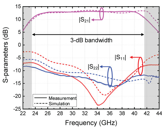
Figure 9.
Measured S-parameters of the full Ka-band amplifier.
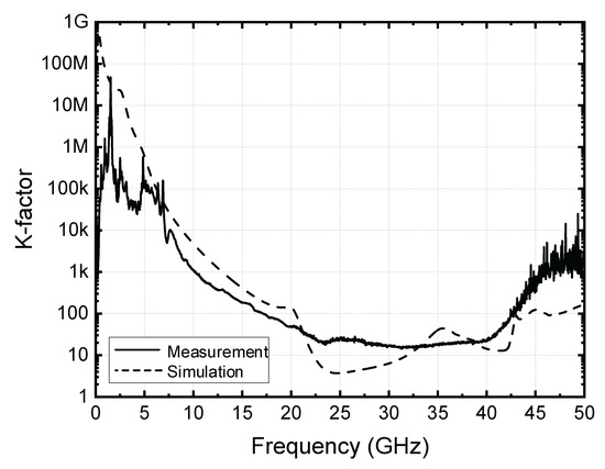
Figure 10.
Stability factor based on the measured S-parameters.
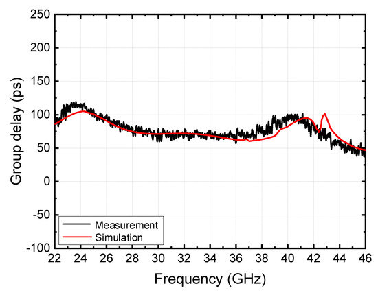
Figure 11.
Measured group delay.
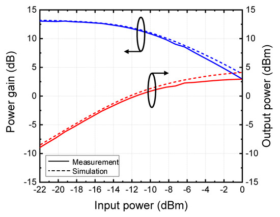
Figure 12.
Measured output power and gain versus input power at 34 GHz.
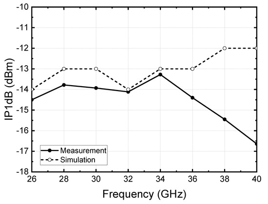
Figure 13.
Measured IP1dB versus frequency.
In Table 2, the measured performances are summarized and compared with those of the previously reported CMOS Ka-band amplifiers. The amplifier in this study exhibited a superior gain flatness in the full Ka-band frequencies to the other state-of-the-art amplifiers.
Table 2.
Performance comparison with previous CMOS-based Ka-band amplifiers.
4. Conclusions
In this research, a full Ka-band amplifier with a flat-gain response was fabricated using a 65 nm CMOS technology. To compensate for the gain roll-off in the upper end of the bandwidth, an inductive neutralization technique was used in the first stage. Neutralization inductance was carefully determined by considering gain and stability. To achieve a wideband flat gain, three CS stages designed at different center frequencies of 26, 34, and 42 GHz were cascaded. Using the frequency staggering technique, we found that the whole amplifier exhibited a flat-gain response of 13 ± 0.2 dB over the full Ka-band frequencies.
Author Contributions
Conceptualization, B.K. and S.J.; methodology, B.K. and S.J.; investigation, B.K. and S.J.; data curation, B.K. and S.J.; formal analysis, B.K. and S.J.; writing—original draft preparation, B.K.; writing—review and editing, S.J.; supervision, S.J.; project administration, S.J.; funding acquisition, S.J. All authors have read and agreed to the published version of the manuscript.
Funding
This study was supported by the Institute of Information and Communications Technology Planning and Evaluation (IITP) grant funded by the Korean government (MSIT) (No. 2021-0-00260, Research on LEO Inter-Satellite Links).
Institutional Review Board Statement
Not applicable.
Informed Consent Statement
Not applicable.
Data Availability Statement
Not applicable.
Acknowledgments
The authors would like to thank the IC Design Education Center (IDEC), Korea, for the chip fabrication and EDA tool support.
Conflicts of Interest
The authors declare no conflict of interest.
References
- Federal Communications Commission FCC 16–89. Available online: https://docs.fcc.gov/public/attachments/FCC-16-89A1.pdf (accessed on 14 July 2016).
- Spectrum for 4G and 5G; Qualcomm: San Diego, LA, USA; Available online: https://www.qualcomm.com/media/documents/files/spectrum-for-4g-and-5g.pdf (accessed on 1 December 2017).
- Chen, H.; Chang, D.; Juang, Y.; Lu, S. A Compact Wideband CMOS Low-Noise Amplifier Using Shunt Resistive-Feedback and Series Inductive-Peaking Techniques. IEEE Microw. Wirel. Compon. Lett. 2007, 17, 616–618. [Google Scholar] [CrossRef]
- Joo, S.; Choi, T.; Jung, B. A 2.4-GHz Resistive Feedback LNA in 0.13 μm CMOS. IEEE J. Solid-State Circuits 2009, 44, 3019–3029. [Google Scholar] [CrossRef]
- Lin, Y.S.; Chen, C.Z.; Yang, H.Y.; Chen, C.C.; Lee, J.H.; Huang, G.W.; Lu, S.S. Analysis and Design of a CMOS UWB LNA with Dual-RLC-Branch Wideband Input Matching Network. IEEE Trans. Microw. Theory Tech. 2010, 58, 287–296. [Google Scholar]
- Perumana, B.G.; Zhan, J.C.; Taylor, S.S.; Laskar, J. A 0.5-6 GHz Improved Linearity, Resistive Feedback 90-nm CMOS LNA. In Proceedings of the 2006 IEEE Asian Solid-State Circuits Conference, Hangzhou, China, 13–15 November 2006; pp. 263–266. [Google Scholar]
- Wang, R.; Lin, M.; Yang, C.; Lin, C. A 1V 3.1-10.6 GHz Full-band Cascoded UWB LNA with Resistive Feedback. In Proceedings of the 2007 IEEE Conference on Electron Devices and Solid-State Circuits, Tainan, Taiwan, 20–22 December 2007; pp. 1021–1023. [Google Scholar]
- Chen, H.; Zhu, H.; Wu, L.; Che, W.; Xue, Q. A wideband CMOS LNA using transformer-based input matching and pole-tuning technique. IEEE Trans. Microw. Theory Tech. 2021, 69, 3335–3347. [Google Scholar] [CrossRef]
- Qin, P.; Xue, Q. Compact wideband LNA with gain and input matching bandwidth extensions by transformer. IEEE Microw. Wirel. Compon. Lett. 2017, 27, 657–659. [Google Scholar] [CrossRef]
- Gonzalez, G. Microwave Transistor Amplifiers Analysis and Design, 2nd ed.; Prentice-Hall: Upper Saddle River, NJ, USA, 1997. [Google Scholar]
- Razavi, B. Design of Analog CMOS Integrated Circuits; McGraw-Hill: Boston, MA, USA, 2016; pp. 173–214. [Google Scholar]
- Trinh, V.; Park, J. A 16.3 dBm 14.1% PAE 28-dB Gain W-Band Power Amplifier with Inductive Feedback in 65-nm CMOS. IEEE Microw. Wirel. Compon. Lett. 2020, 30, 193–196. [Google Scholar] [CrossRef]
- Lei, H.-W.; Wang, Y.; Chiong, C.-C.; Wang, H. A 2.5–31-GHz high gain LNA in 0.15-μm GaAs pHEMT for radio astronomical application. In Proceedings of the Asia–Pacific Microwave Conference (APMC), Yokohama, Japan, 29 November–2 December 2018; pp. 228–230. [Google Scholar]
- Singh, R.; Mondal, S.; Paramesh, J. A millimeter-wave receiver using a wideband low-noise amplifier with one-port coupled resonator loads. IEEE Trans. Microw. Theory Tech. 2020, 68, 3794–3803. [Google Scholar] [CrossRef]
- Zhang, C.; Zhang, F.; Syed, S.; Otto, M.; Bellaouar, A. A low noise figure 28 GHz LNA in 22 nm FDSOI technology. In Proceedings of the 2019 IEEE Radio Frequency Integrated Circuits Symposium (RFIC), Boston, MA, USA, 2–4 June 2019; pp. 207–210. [Google Scholar]
- Gao, L.; Rebeiz, G.M. A 24–43 GHz LNA with 3.1–3.7 dB noise figure and embedded 3-pole elliptic high-pass response for 5G applications in 22 nm FDSOI. In Proceedings of the 2019 IEEE Radio Frequency Integrated Circuits Symposium (RFIC), Boston, MA, USA, 2–4 June 2019; pp. 239–242. [Google Scholar]
- Hedayati, M.K.; Abdipour, A.; Shirazi, R.S.; Cetintepe, C.; Staszewski, R.B. A 33-GHz LNA for 5G wireless systems in 28-nm bulk CMOS. IEEE Trans. Circuits Syst. II Express Br. 2018, 65, 1460–1464. [Google Scholar] [CrossRef]
- Elkholy, M.; Shakib, S.; Dunworth, J.; Aparin, V.; Entesari, K. A wideband variable gain LNA with high OIP3 for 5G using 40-nm bulk CMOS. IEEE Microw. Wirel. Compon. Lett. 2018, 28, 64–66. [Google Scholar] [CrossRef]
- Chauhan, V.; Floyd, B. A 24–44 GHz UWB LNA for 5G cellular frequency bands. In Proceedings of the 2018 11th Global Symposium on Millimeter Waves (GSMM), Boulder, CO, USA, 22–24 May 2018; pp. 1–3. [Google Scholar]
- Yeh, H.; Chiong, C.; Aloui, S.; Wang, H. Analysis and Design of Millimeter-Wave Low-Voltage CMOS Cascode LNA With Magnetic Coupled Technique. IEEE Trans. Microw. Theory Tech. 2012, 60, 4066–4079. [Google Scholar] [CrossRef]
Publisher’s Note: MDPI stays neutral with regard to jurisdictional claims in published maps and institutional affiliations. |
© 2022 by the authors. Licensee MDPI, Basel, Switzerland. This article is an open access article distributed under the terms and conditions of the Creative Commons Attribution (CC BY) license (https://creativecommons.org/licenses/by/4.0/).