Article

Design and Implementation of Quad-Port MIMO Antenna with Dual-Band Elimination Characteristics for Ultra-Wideband Applications

1
Department of Electrical Engineering, School of Engineering, Gautam Buddha University, Greater Noida 201308, India
2
Department of Electrical Engineering, College of Engineering, Princess Nourah Bint Abdulrahman University, Riyadh 84428, Saudi Arabia
3
Department of Computer Sciences, College of Computer and Information Sciences, Princess Nourah Bint Abdulrahman University, Riyadh 84428, Saudi Arabia
*
Authors to whom correspondence should be addressed.
On leave from Gautam Buddha University, Greater Noida, India.
Appl. Sci. 2020, 10(5), 1715; https://doi.org/10.3390/app10051715
Submission received: 4 February 2020 / Revised: 19 February 2020 / Accepted: 24 February 2020 / Published: 2 March 2020
(This article belongs to the Special Issue Passive Planar Microwave Devices )

Abstract

:
A planar, microstrip line-fed, quad-port, multiple-input-multiple-output (MIMO) antenna with dual-band rejection features is proposed for ultra-wideband (UWB) applications. The proposed MIMO antenna design consists of four identical octagonal-shaped radiating elements, which are placed orthogonally to each other. The dual-band rejection property (3.5 GHz and 5.5 GHz corresponding to Wi-MAX and WLAN bands) was obtained by introducing a hexagonal-shaped complementary split-ring resonator (HCSRR) in the radiators of the designed antenna. The MIMO antenna was etched on low-cost FR-4 dielectric substrate of size 58 × 58 × 0.8 mm3. Isolation higher than 18 dB and envelope correlation coefficient (ECC) lesser than 0.07 was observed for the MIMO/diversity antenna in the operating range of 3–16 GHz. The presented four-port UWB MIMO antenna configuration was fabricated, and the experimental results validate the simulation outcomes.

1. Introduction

The use of ultra-wideband (UWB) technology for wireless applications has seen a surge after the Federal Communications Commission (FCC) specified the 3.1–10.6 GHz band as an unlicensed band [1]. Recently, UWB antennas have attracted the focus of RF engineers and researchers due to their extensive usage in sensing networks, cognitive radios, microwave imaging, wearable devices, military applications, wireless personal area networks, and high data rate communication systems. The monopole-based UWB antennas of various shapes and sizes have been explored by the researchers for various applications [2,3]. The features, such as low-profile, miniature size, light-weight, good radiation efficiency, and simple integration into communication devices, make planar monopole antennas a preferred choice for UWB transceiver systems [4]. However, UWB antennas suffer from the disadvantage that radiation can be transmitted to smaller distances only, which is due to the use of low power for transmission, as mentioned by the Federal Communications Commission (FCC) [5]. The limitations of low power and short-range transmission can be encountered using multiple-input-multiple-output (MIMO) technology along with UWB. It uses multiple radiating elements for transmitting and receiving wireless signals, but the placement of multiple elements in a limited space within a communication device/system is a challenge. The close placement of resonating elements will result in poor isolation and high envelope correlation coefficient (ECC), which deteriorates the functioning of the designed system. An inverse relationship exists between the mutual coupling and the space present among the resonating elements. Various methods have been explored and proposed by the researchers for designing MIMO antennas. In literature, different configurations of dual-element antennas have been reported, but these antennas provide limited diversity. The designing of quad-port MIMO systems having four identical radiating elements is more complex as compared to the designing of dual-port systems having two identical elements, due to a higher level of mutual coupling in quad-port systems [6,7].
Moreover, various commercially available devices use Wi-MAX and WLAN bands for performing operations like data transfer, wireless connectivity, etc., which may interfere with the UWB and thus affects the performance of the UWB system. Thus, it is preferable to eliminate these bands for better functioning of the UWB system [8,9]. In the literature, many band-notched UWB MIMO/diversity antennas have been explored [10,11,12,13,14,15,16,17,18]. A MIMO antenna with two G-shaped elements was reported, where isolation between the resonating elements was enhanced by a T-shaped metal strip designed on the ground surface [10]. In [11], a compact MIMO design comprised of a coplanar waveguide-fed (CPW) monopole antenna and a half-slot antenna was presented, where a T-shaped parasitic stub, a protracted Z-shaped stub, a rectangular slot, and a combination of C-shaped slots were implanted to notch 5–6 GHz band. In [12], a small-sized two-port MIMO antenna comprised of square-shaped monopole resonators and a T-shaped metal stub embedded in the ground surface to reduce mutual coupling was proposed. In [13], a MIMO antenna composed of two staircase-shaped resonating elements was reported, where band rejection property was realized by engraving split-ring resonator (SRR) slits on the patch elements. In [14], a planar filtenna with shunt short-circuited stubs and three interdigital edge-coupled patterns was suggested for UWB MIMO applications, where dual notched-band characteristics were realized by introducing a complementary split-ring resonator (CSRR). A small-sized differential stepped-slot MIMO antenna was proposed with notched band rejection capability [15], where four U-shaped stubs were implanted in the radiators to notch the WLAN band. In reference [16], a MIMO antenna consisting of four circular monopole patches and electromagnetic band-gap (EBG) elements was suggested, where four semi-circular ring-shaped slots were engraved on the radiating patches to obtain a notched-band. A four-element UWB MIMO antenna design with a mushroom-like EBG structure to a notch 5.5 GHz band was suggested [17]. In [18], a quad-port UWB MIMO structure with two notched frequency bands was suggested, where the dimensions of the antenna were optimized by using an iterative design method.
In this communication, a planar, compact, MIMO antenna comprising four identical octagonal-shaped resonating elements is proposed. The unit element contains a microstrip line of impedance 50 Ω, octagonal-shaped monopole resonator, and a rectangular-shaped ground surface. A hexagonal-shaped complementary split-ring resonator (HCSRR) was embedded in the monopole antenna patch to notch the interfering Wi-MAX and WLAN frequencies. The MIMO/diversity antenna elements are arranged in orthogonal orientation, and spacing was introduced between them to achieve higher isolation. Metallic strips are also inserted between the monopole elements in order to connect their ground surfaces to obtain common voltage intensity in the MIMO structure. The metallic strips also increase the isolation among four resonators of the MIMO/diversity antenna.

2. Antenna Design

2.1. UWB Antenna Element

The diagrammatic design of the proposed unit antenna element is shown in Figure 1. The unit cell consists of a microstrip line-fed octagonal-shaped resonating element and a rectangular ground plane. An HCSRR is implanted in the octagonal patch of the antenna for notching Wi-MAX (3.5 GHz) and WLAN (5.5 GHz) band frequencies. To obtain better impedance matching, a U-shaped slot is carved from the ground plane of the monopole antenna. The antenna is imprinted on the FR-4 dielectric material of 0.8 mm thickness and relative permittivity of 4.4. An ANSYS HFSS® tool is utilized for simulation, designing, and implementation of the designed antenna. The dimension details of the octagonal monopole element are provided in Table 1.
The antenna design stages are demonstrated in Figure 2. Firstly, an octagonal-shaped radiator (stage-1), fed by a microstrip line of impedance 50 Ω was considered, as displayed in Figure 2a. The radiator was characterized by high eccentricity, which is required for supporting multiple modes in UWB applications. The surface below the antenna radiating patch acted as an unbalanced impedance as it was not grounded. A small U-shaped slot was carved from the ground surface (beneath the microstrip feed line) for providing the required impedance matching among the patch and the feed line (stage-2), as demonstrated in Figure 2b. In Figure 2c, a hexagonal SRR was implanted in the antenna radiator to remove the interfering 5.5 GHz (WLAN) band from the UWB (stage-3). In the next stage, as shown in Figure 2d, an additional hexagonal SRR (opposite to the hexagonal SRR in stage-3) was loaded on the radiator to eliminate interfering 3.5 GHz (Wi-MAX) band signals (stage-4). The lengths of the implanted SRR (outer and inner) can be computed as [19].
S o = 2 π s 1 w 5 0.52 λ g o
S i = 2 π s 3 w 4 0.52 λ g i
λ g = c f r ( 1   ε r ,   e f f )
ε r ,   e f f = ε r + 1 2
where λg and fr denote the guided wavelength and notch-band central frequency, respectively, c denotes the speed of light in vacuum, and εr,eff represents the effective relative permittivity. Figure 3 displays the S11 characteristics of the design steps of the proposed UWB antenna element. A magnified view of the HCSRR is given in Figure 1b, which contains two concentric hexagonal split rings of different dimensions.
Figure 4a,b display the current behavior at notch frequencies 3.5 GHz and 5.5 GHz, correspondingly. From Figure 4a, it can be observed that the concentration of current was higher near the boundaries of the outer hexagonal split-ring, resulting in suppression of the Wi-MAX band. Similarly, Figure 4b shows that a high magnitude current flowed along the boundaries of the inner hexagonal split-ring, which resulted in the elimination of WLAN signals. Therefore, dual band-notched characteristics were achieved by loading an HCSRR in the octagonal radiating patch.

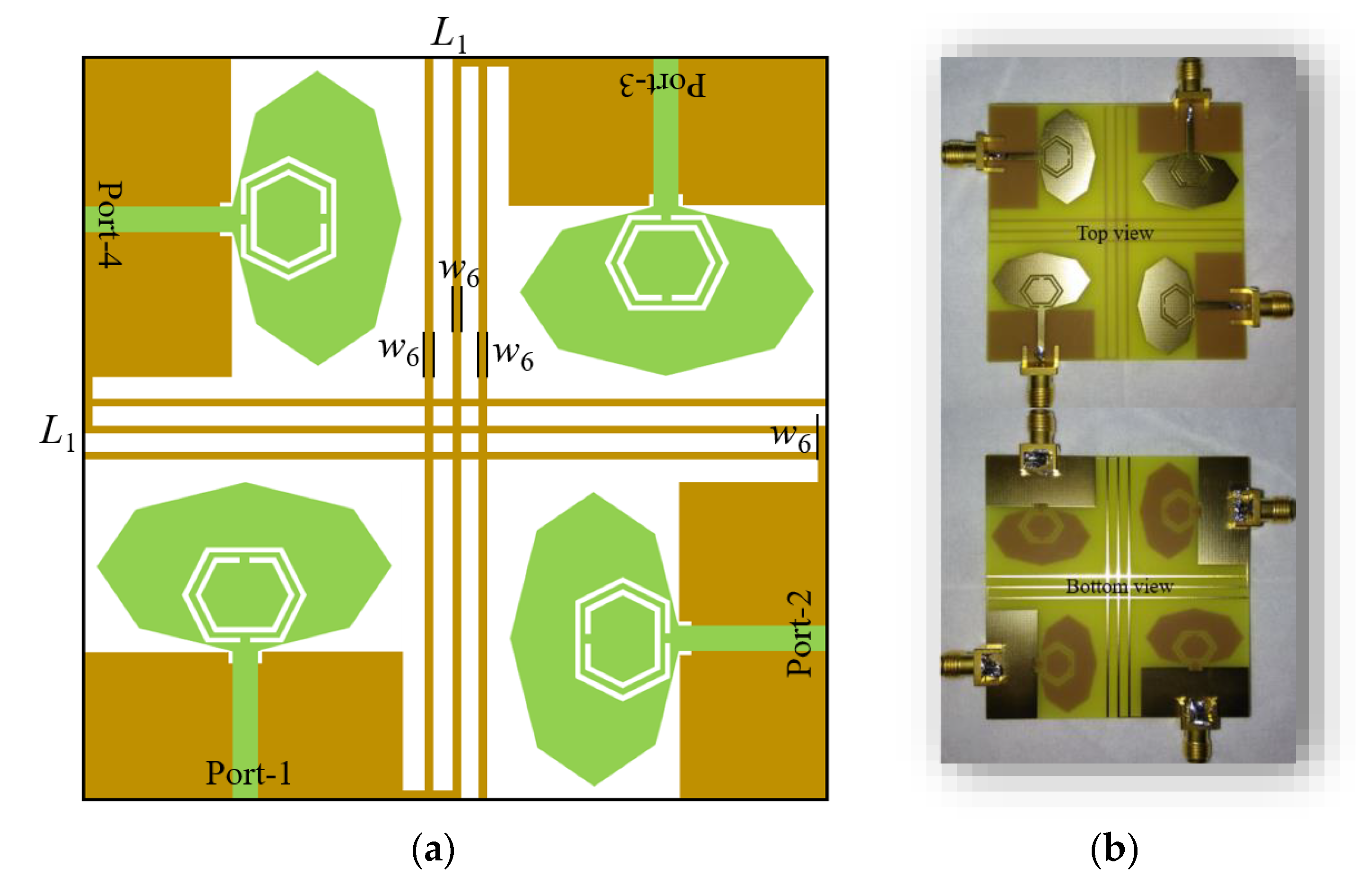
2.2. Quad-Port MIMO Antenna
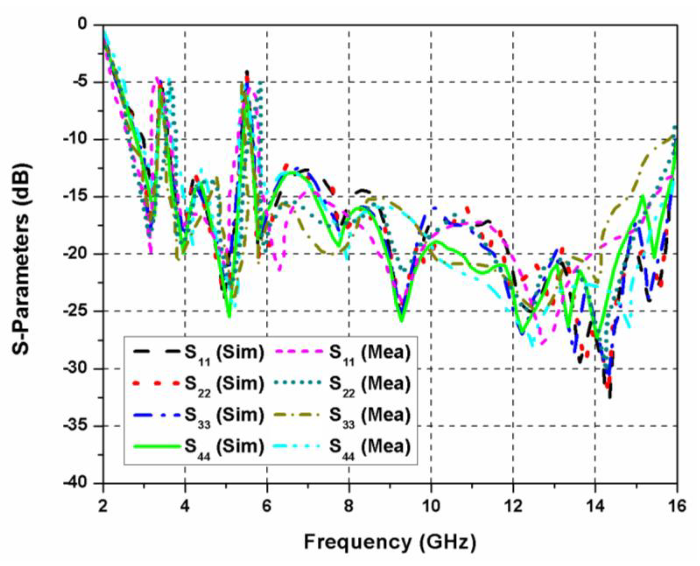
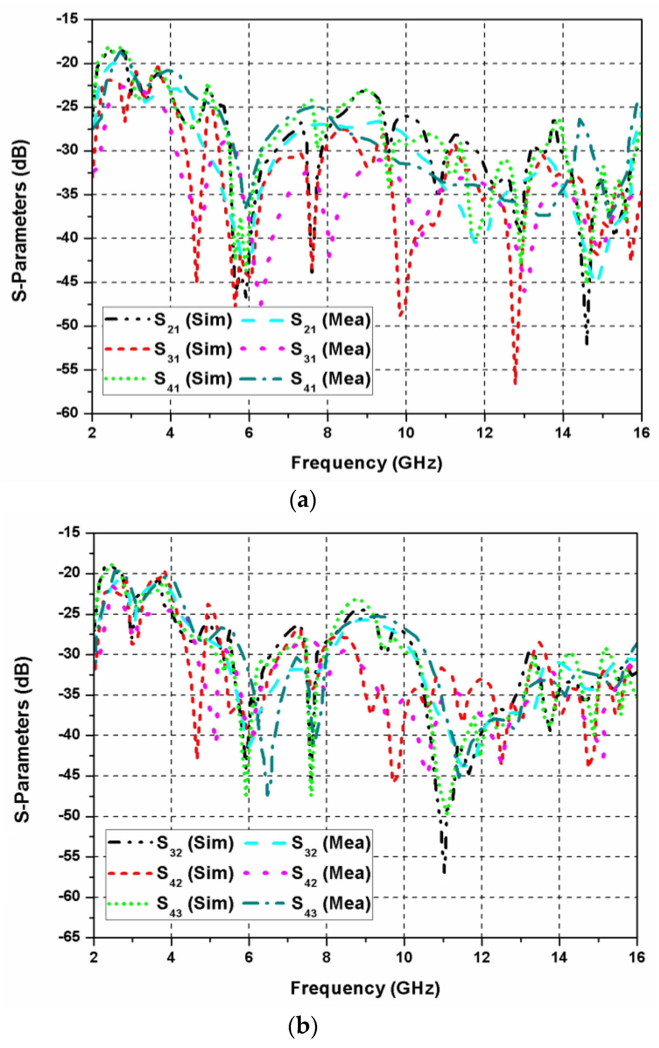
The geometric layout of the MIMO antenna is presented in Figure 5a, and its design dimensions are provided in Table 1. The MIMO design consists of microstrip-line fed octagonal-shaped four identical antenna elements, which are arranged in orthogonal directions to attain superior performance. The antenna feeding points are represented as port-1, port-2, port-3, and port-4, in the layout diagram. Enhanced isolation was achieved as a result of the orthogonal field produced between the adjacent octagonal-shaped radiating elements, consequently, a reduction in inter-element coupling was noticed. However, due to close proximity of the resonating elements, the weak coupling was observed at the lower frequency range, which can be reduced by introducing decoupling elements on the ground surface. Therefore, on the back-side of the dielectric substrate, three metal strips were introduced between the ground patches of the antenna elements to enhance inter-element isolation. The metal strips restrained the current radiated to the adjacent excited elements, thereby enhancing the mutual coupling level. For realizing the optimal decoupling response, the size and spacing among the strips were determined by analyzing multiple simulations and surface current distribution. In addition, these metallic strips united the ground patches of the four radiators to confirm the same voltage in the designed antenna. In a real system, the resonating patches should have the same reference plane to understand the signal level properly. The MIMO system will not work efficiently if isolated ground planes are present [20]. The antenna fabricated prototype is displayed in Figure 5b. The total size of the presented four-port MIMO/diversity antenna is 58 × 58 × 0.8 mm3.
The proposed MIMO antenna design steps are demonstrated in Figure 6. Firstly, as illustrated in Figure 6a, four identical octagonal-shaped resonating elements were arranged orthogonally to each other. Sufficient space was provided between the four radiators to suppress inter-element correlation. In step-2, as shown in Figure 6b, a thin strip was inserted in the middle of the MIMO antenna to reduce mutual coupling further. The thin strip suppresses the inter-element coupling considerably, but more isolation was required between the antenna elements to obtain effective notching and diversity performance. Therefore, as illustrated in Figure 6c, a decoupling structure consisting of two strips was introduced in the center of the MIMO antenna (step-3), which reduces mutual coupling up to −15 dB in the working band.
In addition, to obtain more isolation between the resonating elements, a decoupling element comprised of three metal strips was introduced in the middle of the MIMO antenna (shown in Figure 5). The decoupling element with three metal strips offers isolation greater than 18 dB and also unites the ground planes of the four radiators to confirm the same voltage in the proposed MIMO antenna. The mutual coupling comparison of the three MIMO stages is displayed in Figure 6d.

3. Results

The antenna electrical performance was measured using 50 Ω SMA connectors. The reflection coefficients (simulated and measured) of the designed UWB MIMO antenna at different ports (S11, S22, S33, S44) are shown in Figure 7. While performing measurements at one resonating element, the remaining antenna ports were matched with 50 Ω loads.
The HCSRR embedded in the antenna radiator eliminated the Wi-MAX and WLAN frequencies. The frequency of the elimination bands can be altered by varying dimensions of the HCSRR. The mutual coupling among different resonating elements of the MIMO antenna is illustrated in Figure 8a,b. The inter-element coupling was decreased through an orthogonal arrangement of the resonating elements and by introducing metal strips between their ground planes. Isolation greater than 18 dB was attained for impedance bandwidth range. As displayed in Figure 9, a 7 dBi peak gain was realized in the proposed UWB antenna. A sudden fall in the gain was observed at dual-band rejection frequencies.
The surface-current behaviors at notch frequencies 3.5 GHz and 5.5 GHz are presented in Figure 10a,b, correspondingly, here, all the four elements were excited concurrently. The maximum concentration of current (highlighted in red color) was observed near to the boundary of the outer hexagonal split-ring (Figure 10a), which resulted in Wi-MAX band rejection. Similarly, high current concentration near the boundaries of the inner hexagonal split-ring (Figure 10b), marked the rejection of the WLAN band.
ECC can be used to study the coupling effect between adjacent elements of the antenna. The given expression can be used to calculate ECC values between the first and second ports of a multi-port MIMO system [21].
ρ e = | S 11 * S 12 +   S 21 * S 22 + S 13 * S 32 +   S 14 * S 42 | 2 ( 1 | S 11 | 2 | S 21 | 2 | S 31 | 2 | S 41 | 2 ) ( 1 | S 12 | 2 | S 22 | 2 | S 32 | 2 | S 42 | 2 )
In a similar way, the ECC among remaining antenna elements can also be determined. Figure 11 displays the ECC curves among different elements. ECC was observed to remain below 0.07 for the entire UWB band.
Figure 12 illustrates the co-polar and cross-polar radiation characteristics (simulated and experimental) of the designed MIMO antenna at frequencies 5 GHz, 9 GHz, and 14 GHz. A difference higher than 15 dB was seen among the co-polar and cross-polar pattern curves (in E- and H-planes), which shows the stable functioning of the designed antenna. The co-polar patterns of the E-plane displayed bi-directional behavior while the H-plane co-polar patterns possessed omnidirectional behavior. The simulated and experimental outcomes were found in close proximity. The variations observed between the measured and simulated outcomes were due to high loss tangent, antenna fabrication errors, and soldering of the SMA connectors.
Table 2 lists the comparison of the presented dual-band notched UWB MIMO antenna to other existing UWB MIMO antennas in the literature. The comparison table highlights that the designed antenna has numerous advantages over the previous reported notched-band antennas [10,11,12,13,14,15,16,17,18], with reference to size, bandwidth ratio, inter-element isolation, and the number of radiating patches. The three metal ring-based decoupling technique used for reducing mutual coupling is simple and effective. In the presented MIMO antenna, the notch frequencies (3.5 GHz and 5.5 GHz) were removed by introducing HCSRR in the resonating patch, without engaging any other active elements or filter circuitry. Moreover, the orthogonal orientation of the resonating elements offered better isolation and joined ground patches of the monopole elements offered a common reference voltage.

4. Conclusions

In this article, a small-sized four-port UWB MIMO antenna with dual-band rejection features is presented. The proposed design contains four matching octagonal-shaped resonators arranged orthogonally, and the diagonal elements are arranged anti-parallelly. The antenna showed an isolation >18 dB for the entire operational range. An HCSRR was implanted in the radiating element for notching the interfering Wi-MAX and WLAN frequencies (3.5 and 5.5 GHz, respectively). The simulated and experimental results for gain, S-parameters, isolation, ECC, and radiation patterns were studied. The results validated that the decoupling metal strips used to reduce the inter-element coupling is a simple and efficient approach, and a good diversity response was achieved. The obtained results illustrate that the proposed MIMO antenna could be useful for UWB applications. It can serve as a potential candidate for base station terminals and other wireless communication systems.

Author Contributions

Conceptualization, P.K. and S.U.; methodology, P.K.; software, P.K.; validation, P.K., S.U., and F.A.; formal analysis, P.K.; investigation, P.K.; resources, S.U.; data curation, P.K.; writing—Original draft preparation, P.K.; writing—Review and editing, S.U.; visualization, P.K.; supervision, S.U.; project administration, S.U.; funding acquisition, S.U. and F.A. All authors have read and agreed to the published version of the manuscript.

Acknowledgments

This research was funded by the Deanship of Scientific Research at Princess Nourah Bint Abdulrahman University, Riyadh, Saudi Arabia, through the Fast-Track Research Funding Program.

Conflicts of Interest

The authors declare no conflicts of interest.

References

  1. Federal Communications Commission. First Report and Order, Revision of Part 15 of the Commission’s Rules Regarding Ultrawideband Transmission Systems; Federal Communications Commission: Washington, DC, USA, 2002.
  2. Chen, Z.N.; Ammann, M.J.; Qing, X.M.; Wu, X.H.; See, T.S.P.; Cai, A. Planar antennas. IEEE Microw. Mag. 2006, 7, 63–73. [Google Scholar] [CrossRef]
  3. Liang, J.X.; Chian, C.C.; Chen, X.D.; Parini, C.G. Study of a printed circular disc monopole antenna for UWB systems. IEEE Trans. Antennas Propag. 2005, 53, 3500–3504. [Google Scholar] [CrossRef]
  4. Doddipalli, S.; Kothari, A. Compact UWB antenna with integrated triple notch bands for WBAN applications. IEEE Access 2019, 7, 183–190. [Google Scholar] [CrossRef]
  5. Nekoogar, F. Ultra-Wideband Communications: Fundamentals and Applications; Prentice-Hall: Upper Saddle River, NJ, USA, 2006. [Google Scholar]
  6. Sarkar, D.; Srivastava, K.V. Compact four-element SRR-loaded dual-band MIMO antenna for WLAN/WiMAX/WiFi/4G-LTE and 5G applications. Electron. Lett. 2017, 53, 1623–1624. [Google Scholar] [CrossRef]
  7. Ramachandran, A.; Pushpakaran, S.V.; Pezholil, M.; Kesavath, V. A four-port MIMO antenna using concentric square-ring patches loaded with CSRR for high isolation. IEEE Antennas Wirel. Propag. Lett. 2016, 15, 1196–1199. [Google Scholar] [CrossRef]
  8. Abbas, A.; Hussain, N.; Jeong, M.-J.; Park, J.; Shin, K.S.; Kim, T.; Kim, N. A rectangular notch-band UWB antenna with controllable notched bandwidth and centre frequency. Sensors 2020, 20, 777. [Google Scholar] [CrossRef] [PubMed] [Green Version]
  9. Rahman, M.; Ko, D.-S.; Park, J.-D. A compact multiple notched ultra-wide band antenna with an analysis of the CSRR-tO-CSRR coupling for portable UWB applications. Sensors 2017, 17, 2174. [Google Scholar] [CrossRef] [PubMed] [Green Version]
  10. Toktas, A. G-shaped band-notched ultra-widebandMIMO antenna system for mobile terminals. IET Microw. Antennas Propag. 2017, 11, 718–725. [Google Scholar] [CrossRef]
  11. Tao, J.; Feng, Q. Compact UWB band-notch MIMO antenna with embedded antenna element for improved band notch filtering. Prog. Electromagn. Res. C 2016, 67, 117–125. [Google Scholar] [CrossRef] [Green Version]
  12. Liu, L.; Cheung, S.W.; Yuk, T.I. Compact MIMO antenna for portable UWB applications with band-notched characteristic. IEEE Trans. Antennas Propag. 2015, 63, 1917–1924. [Google Scholar] [CrossRef]
  13. Gao, P.; He, S.; Wei, X.; Xu, Z.; Wang, N.; Zheng, Y. Compact printed UWB diversity slot antenna with 5.5-GHz band-notched characteristics. IEEE Antennas Wirel. Propag. Lett. 2014, 13, 376–379. [Google Scholar] [CrossRef]
  14. Li, W.T.; Hei, Y.Q.; Subbaraman, H.; Shi, X.W.; Chen, R.T. Novel printed filtenna with dual notches and good out-of-band characteristics for UWB-MIMO applications. IEEE Microw. Wirel. Compon. Lett. 2016, 26, 765–767. [Google Scholar] [CrossRef]
  15. Liu, Y.Y.; Tu, Z.H. Compact differential band-notched stepped-slot UWB-MIMO antenna with common-mode suppression. IEEE Antennas Wirel. Propag. Lett. 2017, 16, 593–596. [Google Scholar] [CrossRef]
  16. Wu, W.; Yuan, B.; Wu, A. A quad-element UWB-MIMO antenna with band-notch and reduced mutual coupling based on EBG structures. Int. J. Antennas Propag. 2018, 8490740, 1–10. [Google Scholar] [CrossRef] [Green Version]
  17. Kiem, N.K.; Phuong, H.N.B.; Chien, D.N. Design of compact 4× 4 UWB-MIMO antenna with WLAN band rejection. Int. J. Antennas Propag. 2014, 2014, 539094. [Google Scholar] [CrossRef]
  18. Shehata, M.; Said, M.S.; Mostafa, H. Dual notched band quad-element MIMO antenna with multitone interference suppression for IR-UWB wireless applications. IEEE Trans. Antennas Propag. 2018, 66, 5737–5746. [Google Scholar] [CrossRef]
  19. Patre, S.R.; Singh, S.P. Broadband multiple-input-multiple-output antenna using castor leaf-shaped quasi-self-complementary elements. IET Microw. Antennas Propag. 2016, 10, 1673–1681. [Google Scholar] [CrossRef]
  20. Sharawi, M.S. Current misuses and future prospects for printed multiple-input, multiple-output antenna systems [Wireless Corner]. IEEE Antennas Propag. Mag. 2017, 59, 162–170. [Google Scholar] [CrossRef]
  21. Blanch, S.; Romeu, J.; Corbella, I. Exact representation of antenna system diversity performance from input parameter description. Electron. Lett. 2003, 39, 705–707. [Google Scholar] [CrossRef] [Green Version]
Figure 1. Proposed octagonal-shaped monopole antenna: (a) schematic layout; (b) enlarged view of the hexagonal-shaped complementary split-ring resonator (HCSRR).
Applsci 10 01715 g001
Figure 2. Octagonal-shaped monopole antenna design steps: (a) stage-1; (b) stage-2; (c) stage-3; (d) stage-4.
Applsci 10 01715 g002
Figure 3. Simulated reflection coefficients comparison of the evolution steps.
Applsci 10 01715 g003
Figure 4. Surface current distributions at (a) 3.5 GHz; (b) 5.5 GHz.
Applsci 10 01715 g004
Figure 5. Proposed UWB MIMO antenna: (a) geometric layout; (b) prototype.
Applsci 10 01715 g005
Figure 6. Proposed UWB MIMO antenna design steps: (a) step-1; (b) step-2; (c) step-3; (d) mutual coupling comparison.
Applsci 10 01715 g006
Figure 7. S-parameters (simulated and measured) of the MIMO antenna.
Applsci 10 01715 g007
Figure 8. S-parameters (simulated and measured) of the MIMO antenna at (a) port-1; (b) other ports.
Applsci 10 01715 g008
Figure 9. Simulated and measured gain of the proposed antenna.
Applsci 10 01715 g009
Figure 10. Current distributions at (a) 3.5 GHz; (b) 5.5 GHz.
Applsci 10 01715 g010
Figure 11. Envelope correlation coefficient (ECC) of the proposed four-port ultra-wideband (UWB) MIMO antenna.
Applsci 10 01715 g011
Figure 12. Radiation characteristics of the designed antenna at: (a) 5 GHz in H-plane; (b) 5 GHz in E-plane; (c) 9 GHz in H-plane; (d) 9 GHz in E-plane; (e) 14 GHz in H-plane; (f) 14 GHz in E-plane.
Applsci 10 01715 g012
Table 1. Parameter details of the unit element and multiple-input-multiple-output (MIMO) antenna.
ParameterDimension (mm)ParameterDimension (mm)
L26w11
W24s43.5
a5.7w22.5
b8w30.4
f11.25w41
s15w51
s24.5L158
s34w60.5
Table 2. Comparison among the presented MIMO antenna and the previously reported band-notched UWB MIMO antennas.
Ref.Element NumberBandwidth (GHz)Size of the Antenna (mm3)Notch Band NumberNotched Frequency (GHz)Isolation (dB)ECC
[10]22.2–13.3550 × 82 × 1.614.4–6.2>15<0.04
[11]23.1–10.630 × 22 × 0.815–6>15<0.05
[12]23.1–1122 × 36 × 1.615.15–5.85>15<0.1
[13]22.5–1248 × 48 × 0.815.5>15<0.005
[14]23.1–10.6535 × 68 × 123.35–3.55, 5.65–5.95>20<0.002
[15]42.95–10.844 × 44 × 1.615.10–5.95>15.5<0.1
[16]43–16.260 × 60 × 1.614.6>17.5<0.4
[17]42.73–10.6860 × 60 × 1.615.36–6.34>15<0.5
[18]42–15100 × 100 × 1.623.5, 5.5>20<0.1
Prop.23–1658 × 58 × 0.823.5, 5.5>18<0.07

