Article

Selective Disintegration–Milling to Obtain Metal-Rich Particle Fractions from E-Waste

1
Institute of Physics, University of Latvia, 32 Miera Street, LV-2169 Salaspils, Latvia
2
Faculty of Civil Engineering, Riga Technical University, 21/1 Azenes Street, LV-1048 Riga, Latvia
3
ZTF Aerkom SIA, 32 Miera Street, LV-2169 Salaspils, Latvia
4
Institute of Materials and Surface Engineering, Faculty of Materials Science and Applied Chemistry, Riga Technical University, P. Valdena Street 3/7, LV-1048 Riga, Latvia
5
Rudolfs Cimdins Riga Biomaterials Innovations and Development Centre of RTU, Institute of General Chemical Engineering, Faculty of Materials Science and Applied Chemistry, Riga Technical University, 3 Pulka Street, LV-1007 Riga, Latvia
6
Department of Mechanical and Industrial Engineering, Tallinn University of Technology, Ehitajate Tee 5, 19086 Tallinn, Estonia
7
Life Sciences and Technologies Department, Latvia of University, Svetes Street, LV-3001 Jelgava, Latvia
8
Latvian Maritime Academy, Flotes Street 12 k-1, LV-1016 Riga, Latvia
9
Institute of Solid State Physics, University of Latvia, 8 Kengaraga Street, LV-1063 Riga, Latvia
*
Author to whom correspondence should be addressed.
Metals 2022, 12(9), 1468; https://doi.org/10.3390/met12091468
Submission received: 21 July 2022 / Revised: 22 August 2022 / Accepted: 26 August 2022 / Published: 1 September 2022
(This article belongs to the Special Issue Metal Recovery and Separation from Wastes)

Abstract

:
Various metals and semiconductors containing printed circuit boards (PCBs) are abundant in any electronic device equipped with controlling and computing features. These devices inevitably constitute e-waste after the end of service life. The typical construction of PCBs includes mechanically and chemically resistive materials, which significantly reduce the reaction rate or even avoid accessing chemical reagents (dissolvents) to target metals. Additionally, the presence of relatively reactive polymers and compounds from PCBs requires high energy consumption and reactive supply due to the formation of undesirable and sometimes environmentally hazardous reaction products. Preliminarily milling PCBs into powder is a promising method for increasing the reaction rate and avoiding liquid and gaseous emissions. Unfortunately, current state-of-the-art milling methods also lead to the presence of significantly more reactive polymers still adhered to milled target metal particles. This paper aims to find a novel and double-step disintegration–milling approach that can provide the formation of metal-rich particle size fractions. The morphology, particle fraction sizes, bulk density, and metal content in produced particles were measured and compared. Research results show the highest bulk density (up to 6.8 g·cm−3) and total metal content (up to 95.2 wt.%) in finest sieved fractions after the one-step milling of PCBs. Therefore, about half of the tested metallic element concentrations are higher in the one-step milled specimen and with lower adhered plastics concentrations than in double-step milled samples.

Graphical Abstract

1. Introduction

Recyclability and reusability of the materials are highly relevant to modern trends and manufacturing technologies [1]. All industries must reduce any waste significantly by implementing a computer-controlled manufacturing approach. These technologies radically minimize waste by reusing powders and filaments [2]. These benefits decrease manufacturing costs from micron-sized equipment manufacturing up to large-volume industries such as mining [3], shipbuilding [4], and civil engineering [5,6]. However, manufacturers typically produce electronic products and components from ecologically unfriendly materials [7,8]. Therefore, researchers meet the high demand for a novel technique to ensure rapid and cost-effective recycling of electronic waste (e-waste).
About 53.6 Mt of e-waste was generated in 2019, as reported by the Global E-waste Monitor 2020. From these, waste printed circuit boards (PCBs) represent the most economically attractive portion and account for about 3% of the total e-waste [9]. Therefore, PCBs recycling is a business opportunity with a high potential to obtain revenue from growth in the extraction and reuse of precious and base metals, such as gold, silver, and copper [10]. In addition, PCBs contain one of the highest concentrations of rare and precious metals (RPM). Therefore, such waste has the potential to become a sustainable source of RPM for the manufacturing of future generation electronic equipment [11].
The traditional treatment of PCBs includes cutting processes with the help of cutting/shredder mills or a combination of low-intensity impacts, shear, and abrasion with hammermills. However, both methods have significant drawbacks [12,13]. The composition of PCB is complex, wear-resistant, and creates highly abrasive particles during cutting processes. Cutting blades passes through all layers of the PCB composites, which consist not only of epoxy resins and fiberglass but also of robust and malleable metals and alloys, as well as ceramics. The presence of such components leads to high wear of the cutting edges [14]. Worn equipment reduces the efficiency of separating PCB components and requires costly maintenance. Reducing the size of the pieces does not change the structure of the composite, which remains predominantly solid/unbroken [15] with a relatively small area of uncovered precious metals.
As opposed to traditional methods, the high-intensity impact generates high stresses in the structure of PCBs. In addition, these impacts destroy bonding between adhered layers such as resin and fiberglass (less mechanically resistant materials). Additionally, the rapid release and uncovering of the metallic fraction (MF) and non-metallic fraction (NMF) phases [16] occurs. Therefore, the extractor can achieve more efficient further separation by releasing high-quality metal concentrate or exposing a large surface area for the increased possibility/acceleration of chemical reactions [17]. Thus, impact selectivity can achieve a high fragmentation level and becomes the main factor for the mechanical enrichment of target metals. Furthermore, such selective disassembly is less energy consuming and saves the remaining components of the PCB composite from excessive grinding and conversion into technological emissions [18].
PCBs are complex composite materials that consist directly of a multilayer PCB plate, solder, and PCB components [19]. The PCB’s plate generally consists of three layers that are heat laminated together into a single layer. Typically, these are silkscreen, solder mask, copper, and substrate [20]. PCB components are a general term for various components, such as capacitors, resistors, transistors, and other electronic devices. These components include connectors, contacts, fasteners, and many other components attached and connected to a PCB [21].
The typical substrate of the PCB is made of fiberglass and is also known as FR4 (letters FR mean “fire-retardant”). FR-4 glass epoxy is a popular and versatile high-pressure thermoset plastic laminate with an excellent strength-to-weight ratio. This substrate layer provides a solid base for PCBs. However, the thickness may vary depending on the expected PCB’s application and service conditions. The standard thickness of four-layer boards is about 1.6 mm [22].
The second layer of PCB is copper, typically laminated onto the substrate by supplying heat to the adhesive. The copper layer is relatively thin to ensure high electrical conductivity with the lowest possible heat generation. Several boards contain the sandwich of two copper layers on opposite sides of the substrate. Manufacturers usually produce cheaper electronic devices of single copper layered PCBs. The standard level of copper thickness on plane layers is about 35 µm [19].
The PCB’s solder mask provides the visually observable green color. However, sometimes solder masks are designed to give the appearance in other colors, such as brown, red, or blue. The solder mask is also known as a liquid photo imageable solder mask [23]. The solder mask’s purpose is to prevent molten leakage [19]. The metal that facilitates the transfer of current between the board and any attached components is solder, which also serves a dual purpose due to its adhesive properties [24].
The main task for the mechanical processing of PCBs is the separation of PCBs into constituent elements by following or immediate isolation from each other. Therefore, destroying the mechanical bonds between these elements is essential to increase the separation process efficiency [25]. This separation is required to create concentrates of metals and non-metals to facilitate the access of reagents to the exposed surfaces. The most significant and protruding parts (metal and ceramic components) are primarily exposed to abrasion and shear. This effect results in the waste of additional energy and material from the wear of grinding media. This factor accompanies the unnecessary grinding of metal and ceramic components and materials’ ineffective mixing/heating [26]. One of the most widely used e-waste recycling methods is pyrolysis. However, high brominated antipyrine concentration causing a release of toxic gases is the method’s main disadvantage [27]. Currently, manufacturers add the compound PCB to reduce the flammability of computer components in case of fire [28].
PCBs in common could contain up to 30 wt.% polymers, 30 wt.% ceramics, and 40 wt.% metals [29]. Detailed composition by fractions was investigated by Roberto et al. and is represented in Table 1 [30].
However, certain PCB elements contain several precious metals at much higher concentrations. For example, the content of Au, Ag, and Pd in the contact group, connection slots, interfaces, and the board surface range from 180 to 3695 mg·kg−1, from 809 to 12,321 mg·kg−1, and from 96 to 118 mg·kg−1, respectively [31]. As shown above, PCBs contain a significant concentration of valuable and expensive metals. However, along with them, a typical PCB contains up to 70 wt.% non-metallic components made of ceramics, plastics, and fiberglass. These components are part of the textolite. Therefore, developing an efficient method for the preliminary separation of these components is necessary. In addition, material recyclers are interested in preventing the formation of large amounts of liquid or gaseous phases during waste pyrolysis.
Industry experts frequently research and implement new methods for more efficient PCB pretreatment for valuable metals extraction. Reviewed literature shows a general division of PCB pretreatment by mechanical and solvent-based methods [27,32,33,34].
Y. Zhou and K. Qiu, in their publication, have reported a new process of “centrifugal separation +vacuum pyrolysis” to recover solder and organic materials from wasted PCBs [34]. This approach has exhibited the relatively complete separation of solder from PCBs with the help of centrifugal equipment, heated at 240 °C, and the rotating drum set at 1400 rpm for 6 min intermittently. The results of vacuum pyrolysis showed that the PCB without solder pyrolyzed to form an average of 69.5 wt.% solid residue, 27.8 wt.% oil, and 2.7 wt% gaseous phase [34]. This method effectively separates microchips and other functional elements from PCB by removing the solder. However, researchers have admitted that multilayer PCBs avoid complete Cu extraction by further processing steps. Additionally, the pyrolysis process generates significant volumes of toxic organic gases.
M. Tatariants et al. have described a ball milling process to produce a powder exhibiting high fineness from the crushed PCBs [32]. The authors have set the ball mill’s frequency at 20 Hz for 60 min. Such an approach resulted in micro-scaled PCBs powder. Obtained powder consisted of three phases: metal particles with adhered fragments of epoxy resin, fiberglass particles partially covered with epoxy resin, and fiberglass–metal–epoxy composite agglomerates.
Researchers have reported the use of organic solvents, such as dimethylformamide [32], dimethyl sulfoxide (DMSO), and N, N-dimethyl pyrrolidone [33] as efficient tools for brominated epoxy resins removal from PCB’s structure. However, these methods also require other subsequential treatment methods, such as milling, air-flow separation, etc.
Size reduction by disintegration–milling is one of the state-of-the-art PCBs mechanical pretreatment approaches. Various solutions can be mentioned as effective analogues, which still demand improvements or alternative solutions to achieve reliable pretreatment result from e-wastes with variable compositions.
A 3.25 mm fraction particle production from PCBs with the help of a rotary cutting shredder and a subsequent three-stage grinding process in the ceramic ball mill allows for manufacturing particles with sizes down to 125 µm [35]. However, the two-stage PCBs crushing into a rotary cutting shredder down to 3.35 mm, then size reduction down to about 1 mm in a four-bladed rotary cutting shredder, and final grounding with the help of an ultra-centrifugal mill (Retsch ZM 200, Retsch GmbH, Haan, Germany,) allowed for the production of particles with sizes up to 250 µm prior to use for leaching tests [36]. At the same time, the PCB hammer-crushing and grounding with the help of an ultra-centrifugal mill (Retsch ZM 200) provides the production of particles with fraction sizes of 4 mm–212 μm) [37]. Finally, the grounding of PCBs, preliminarily cut into 2 mm pieces, with the help of an LM1-M ring mill (LabTechnics Australia, Victoria, Australia), allowed for the production of particles sieved into <365, 365–500, and 500–750 μm with the help of the Retsch AS200 control sieve shaker (Retsch GmbH, Haan, Germany) [38]. All these methods characterize an inefficient multi-step milling approach with high-energy and human workload consumption.
The present article aims to reveal the milling rate’s effect on the properties of mechanically disintegrated PCBs. The idea is to apply mechanical disintegration as the pre-treatment method to increase the content of recovered valuable metals from specific fractions of disintegrated PCBs. The studied milling process provides the formation of a wide range of particle sizes. The work demonstrates the dependence of common and valuable metal contents on the size of obtained disintegration–milled particles. Therefore, entrepreneurs can use this approach in various manufacturing technologies for further processing the extracted valuable metals. Furthermore, recycling companies can scale up and implement the demonstrated technology in hydrometallurgical and pyrometallurgical processes.

2. Materials and Methods
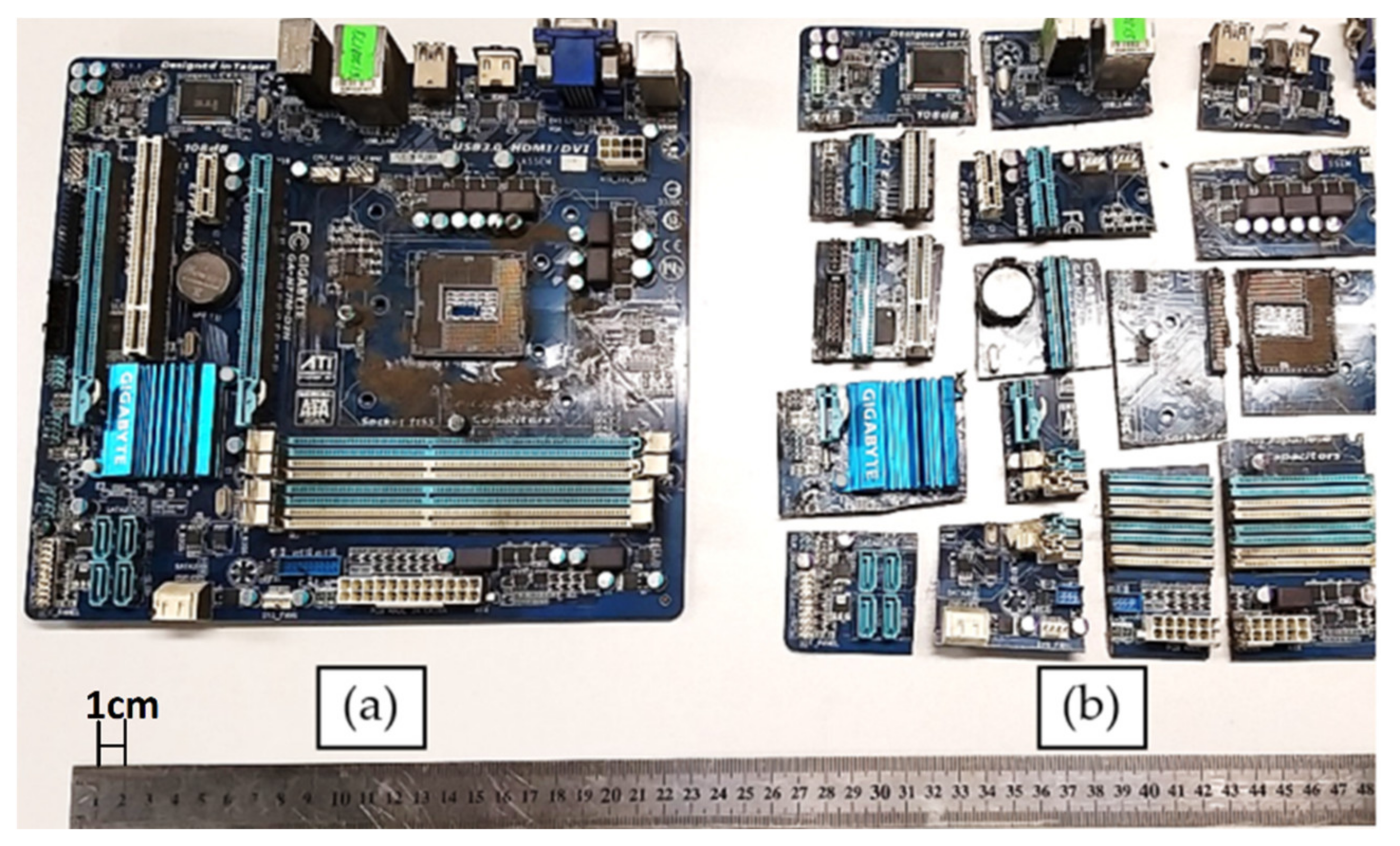
2.1. Used Materials

The article’s authors used PCB waste consisting of disassembled personal computer motherboards (produced by the GIGA-BYTE Technology Co., Ltd., New Taipei City, Taiwan, from 2010 to 2015) without central processors. An operator cut a total of 6 kg PCBs into rectangular-shaped pieces with side lengths from about three up to 6 cm and subjected them to disintegration–milling experiments, as shown in Figure 1a,b.
Disassembly was conducted manually at room temperature to avoid potentially harmful emissions [39].

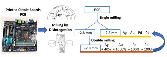
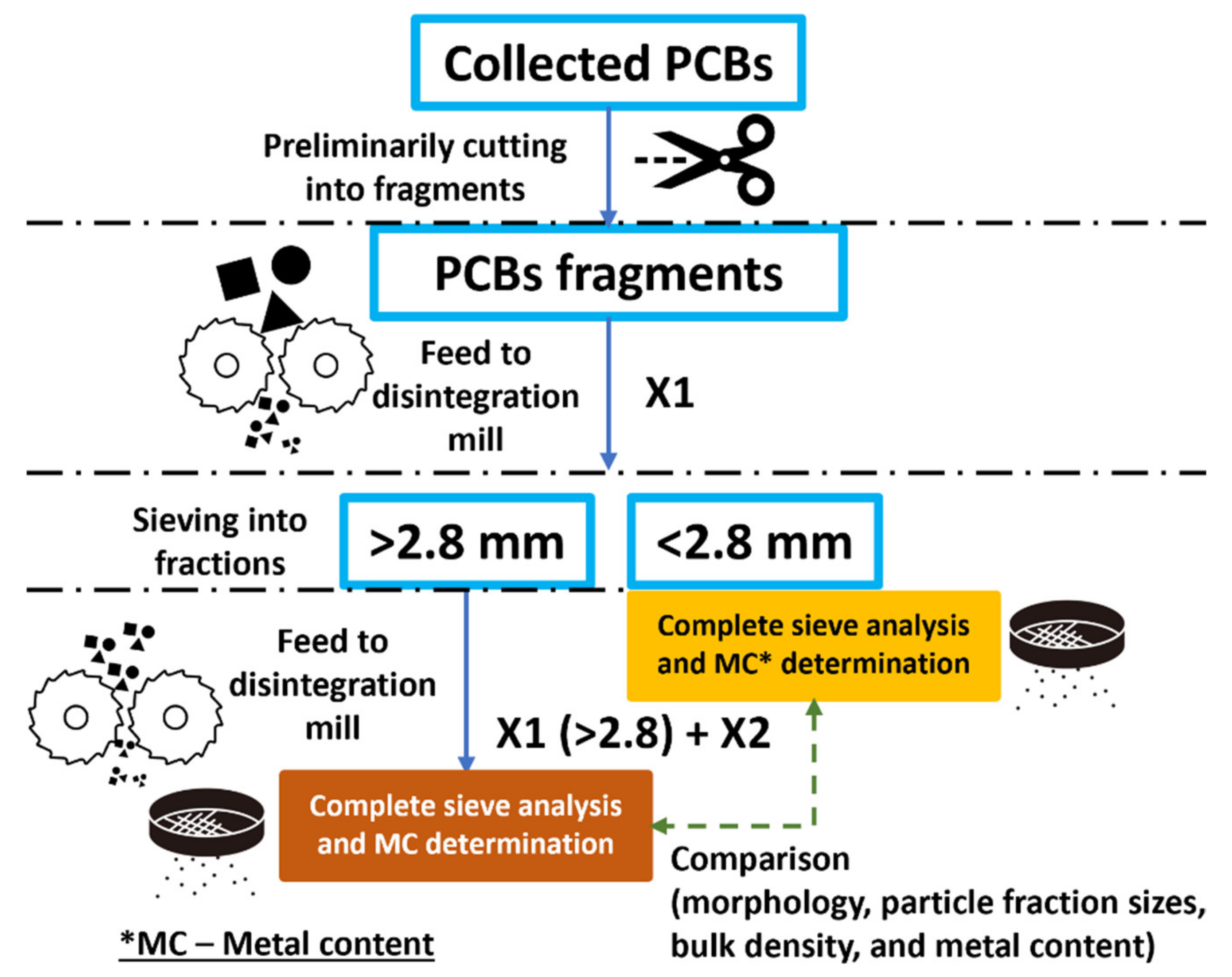
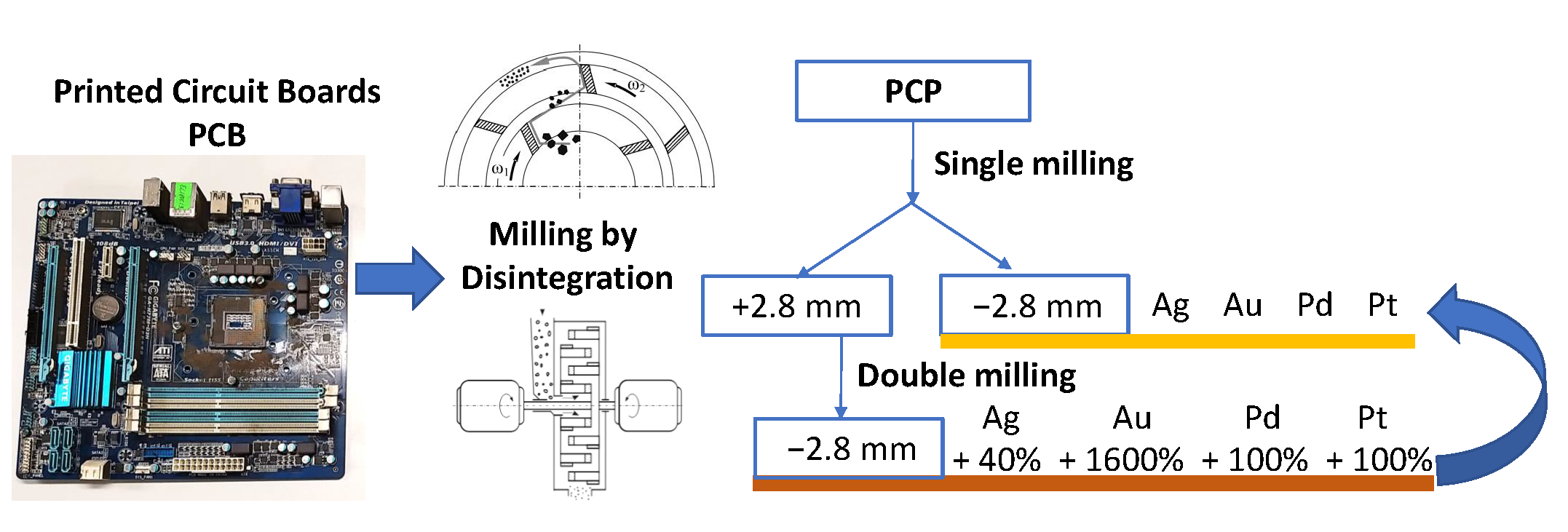
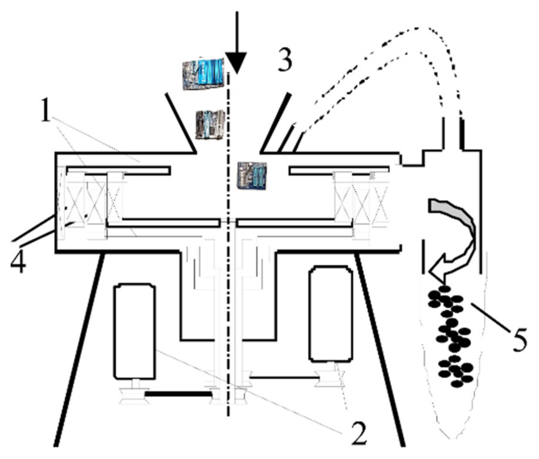
2.2. Applied Milling Procedure and Used Testing Equipment

The high-energy semi-industrial disintegration–milling system DSL-350 (Tallinn University of Technology, Tallinn, Estonia), specially designed for processing mechanically durable materials [40,41,42], was used to grind fragments of PCBs into finer particles. The device is grinding materials by collisions. Supplied particles collide with surfaces of grinding bodies. As a result, the intensive pressure wave propagates inside the target particles. The resulting values of stresses exceed material strength. The specification of the disintegration–milling device is demonstrated in Table 2.
The principal scheme of milling equipment—centrifugal-type disintegrator mill DSL-350 is shown in Figure 2.
Collected PCBs were preliminarily cut into smaller fragments (see Figure 1b) to feed into the disintegration–milling device. Next, the author carried out targeted mechanical cutting (slicing) to avoid damage to the main elements on the surfaces of PCBs. Therefore, only the largest contact groups were cut in half, as demonstrated in Figure 1b. Next, the operator used the obtained pieces with intact elements to investigate the effect of one and double-step disintegration–milling on target metals contents. Finally, the authors selected the disintegration–milling procedure for producing powder from the PCBs, as presented in Figure 3.
An operator milled sliced PCBs (see Figure 1a) once as raw materials. Obtained particles smaller than 2.8 mm were subjected to metal analysis and designated as X1 (see Figure 3). Subsequently, particles bigger than 2.8 mm were subjected to repeated milling and designated as X1 (>2.8) + X2 (see Figure 3).
Determination of particle size distribution was carried out with the help of the vibratory sieve shaker Analysette 3 PRO (FRITSCH GmbH Idar-Oberstein, Germany). Materials with particle sizes up to about 12.5 mm were fractioned using sieves with opening sizes of 0.09, 0.18, 0.35, 0.71, 1.40, 2.80, 5.60, and 11.20 mm. An operator measured the bulk density with the help of the bulk density tester (Scott volumeter, according to ASTM B 329-98, Copley, Nottingham, UK) for each fraction of sieved samples X1 and X1 (>2.8) + X2. An optical microscope (KEYENCE VHX-2000, Keyence Inc, Osaka, Japan) was used to study the morphology of the obtained fractions.
Metal content (MC) changes (in %) from one-step (X1, designated as MCone-step) to double-step (X1 (>2.8) + X2, designated as MCdouble-step) milling PCB by fractions calculated by Equation (1):
M C o n e s t e p M C d o u b l e s t e p M C d o u b l e s t e p · 100   %

2.3. Applied Method for Metal Content Determination

Quantitative determination of MC in disintegration–milled and sieved fractions of raw material was performed with the help of inductively coupled plasma atomic emission spectroscopy (ICP-OES, Thermo scientific iCAP 7000 series, Thermo Fisher Scientific Inc., Waltham, MA, USA).
First, a representative sample was prepared using the quartering method, and chemical leaching was carried out. An aqueous solution of 6M HCl (V = 50 mL) was added to the powder sample’s weight of 500 mg (±0.5 mg). The mixture was boiled until a wet residue formed. Subsequently, the same treatment approach was carried out in two portions of aqua regia (HCl:HNO3 = 3:1, V = 40 mL). An excessive amount of HNO3 was removed by adding concentrated HCl during the boiling process. The resulting wet residue was transferred to the filter with a 3M HCl solution and washed accurately. The resulting filtrate was brought up to a volume of 100 mL with 3M HCl solution. Afterward, the obtained solution was analyzed using ICP-OES (PerkinElmer Polska sp. z o.o., Kraków, Poland). To evaluate the metal content, it is necessary to determine the non-metallic component. In the sample under study, the filter’s undissolved residue (non-metallic element) was washed with distilled water to pH ≈ 5–6, dried at 105 °C, and weighed.

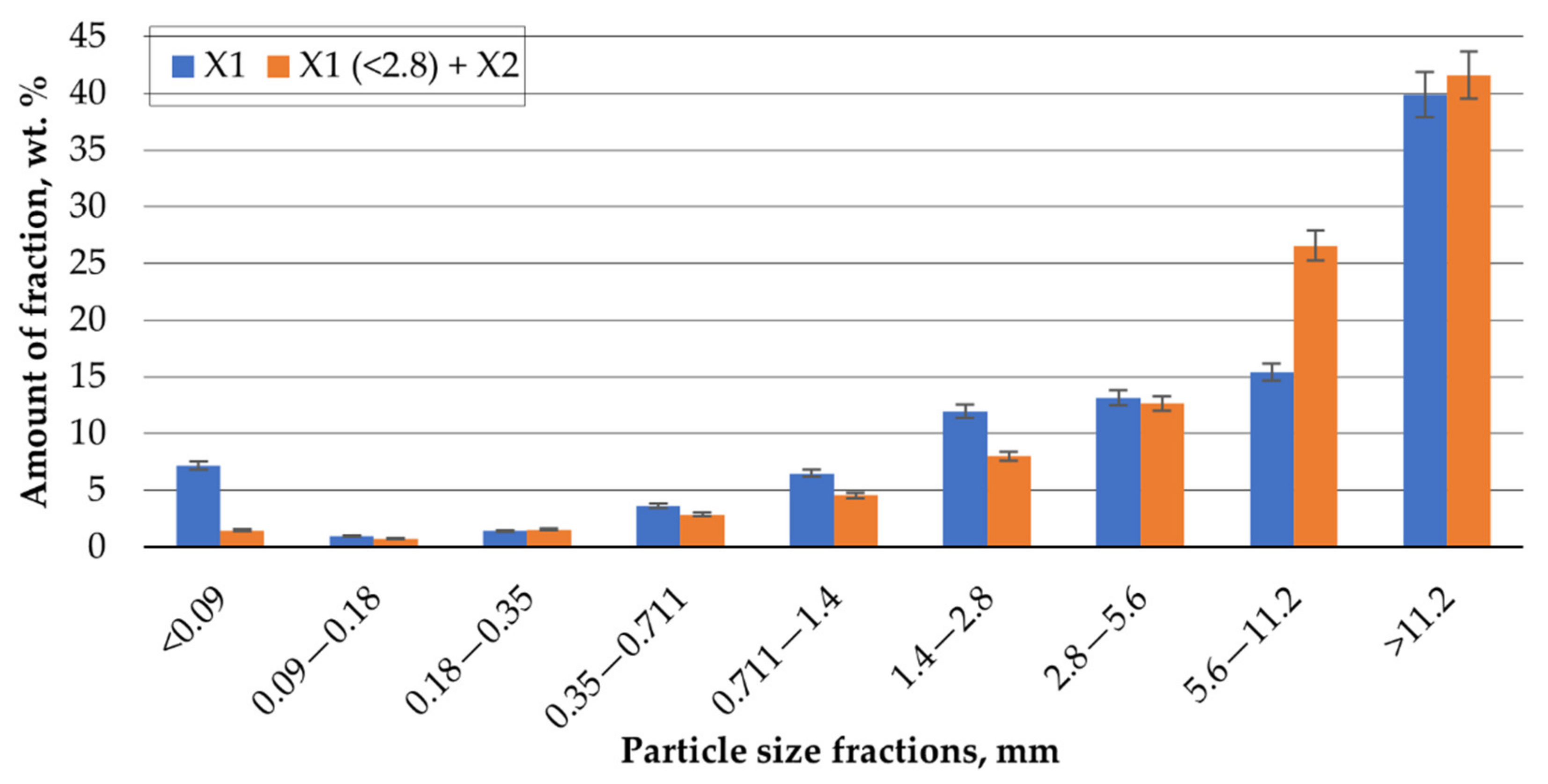
3. Results and Discussion

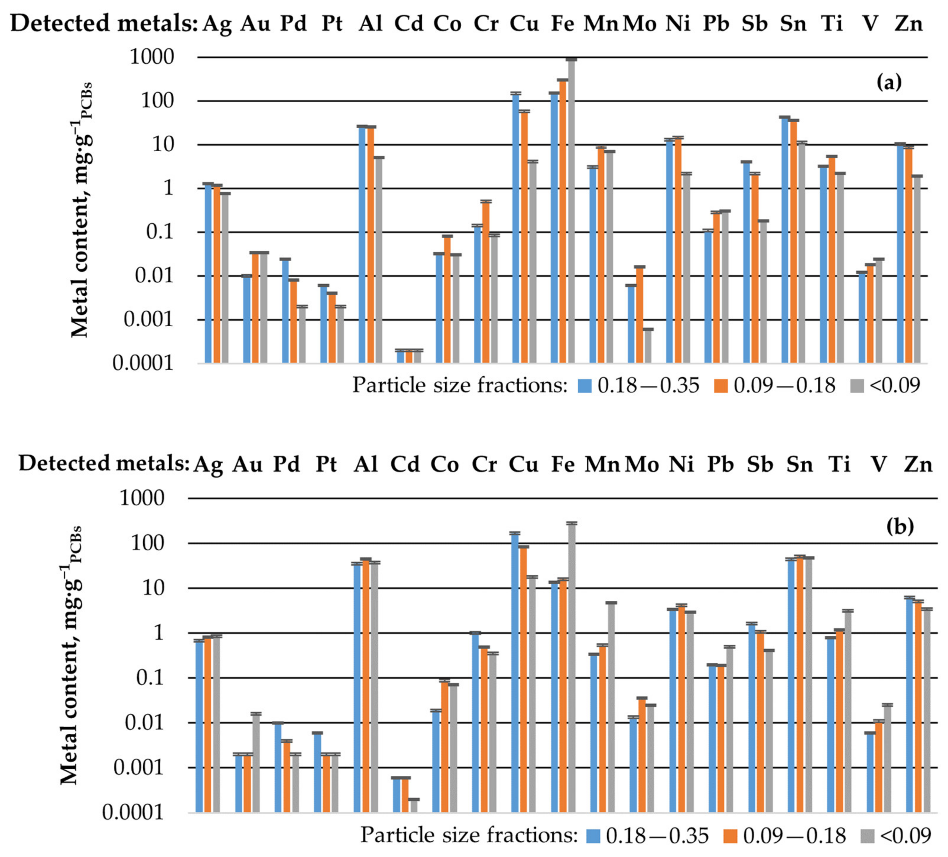
3.1. Metal Content in Disintegration-Milled PCBs Fractions

The correlation between the determined MC and bulk densities in the milled PCB is presented in Table 3. The bulk density of specimen X1 gradually increases from 0.3 to 6.8 g·cm−3 by decreasing the sieved fraction size from 2.8–5.6 mm down to <0.09 mm. Measured bulk density (up to 6.8 g·cm−3) correlates with an increase in MC (up to 95.2 wt.%), which indicates the positive effect of the brittleness of metals on disintegration–milling performance. The fractions from 0.09 to 0.35 mm can be attributed to high metal content with the most of ceramic impurities due to relatively high bulk densities from 4.9 to 6.8 g·cm−3 At the same time, more elastic–plastic composites remain less intact and significantly reduce the densities of largest sieved fractions.
Double milling of residual fraction from specimen X1 with particle sizes above 2.8 mm significantly decreases MC by about 120% in specimen’s X1 (>2.8) + X2 fraction of 0.09–0.18 mm, as compared to the same fraction’s MC of the specimen X1. In addition, double milling also leads to about twice lower MC in case of each fraction from <0.09 (50.6 wt.%) to 0.711 mm (8 wt.%), as compared to the specimen X1. This result obviously demonstrates plastic and ceramic impurities, which also significantly lowers bulk densities more typical for most ceramics (2.23 g·cm−3) and plastics with relatively high content of ceramic and metal impurities (0.35 to 0.84 g·cm−3).
Therefore, higher concentrations of metals can be twice efficiently recovered from one-step milled fractions with sizes larger than 0.35 mm after the first disintegration–milling procedure. In addition, it seems that the idea of combining the exact fraction sizes from samples X1 and X1 (>2.8) + X2 should be performed by preliminarily removing mechanically separated plastics from the double-step milled materials.
Therefore, most promising fractions of <0.09, 0.09–0.18, and 0.18–0.35 mm were chosen for the determination of Ag, Au, Pd, Pt, Al, Cd, Co, Cr, Cu, Fe, Mn, Mo, Ni, Pb, Sb, Sn, Ti, V, and Zn contents [43], as demonstrated in Figure 4a,b.
The results show that the MC varies depending on the stages of disintegration–milling and the fractional particle size. Plastic particles significantly decrease the fraction bulk density and strongly correspond to reducing the metal content in corresponded fraction.
Thus, sample X1 exhibit notably higher MC in Ag, Au, Fe, and Mn cases. Of these, recovering precious Au (from 0.01 to 0.034 mg·g−1) is the most exciting and complicated process and requires chemicals that can be contaminated by side undesired side reactions. Therefore, the Au recovery from large volumes of one-step milled PCBs may provide higher economic feasibility than the recovery of the same metals from sample X1 (>2.8) + X2.
Conversely, sample X1 (>2.8) + X2 exhibits higher concentrations of Cd (from 0.0001 to 0.0006 mg·g−1), Cr (from 0.35 to about 1 mg·g−1), and Mo (from 0.0134 to 0.025 mg·g−1), as compared to the sample X1. However, the beneficial recovery of these elements also requires large PCB volumes.
PCBs contain more than ten-fold purer precious metals compared to ore minerals, relatively rich with the same valuable metal atoms. Therefore, collecting PCBs to recover valuable metals is a crucial part of urban mining [43]. Additionally, the well-developed PCBs collection and recovery management can help avoid the leakage of environmentally harmful metals (e.g., Cr, Pb, Cd, etc.) into the soil, natural waters, and other places where oxidation into harmful compounds and absorption by living organisms may occur.
A better overview of the comparison between MC (in %) in one and double-step milled PCB samples by fractions (calculated according to Equation (1)) is demonstrated in color in Table 4. Results show the benefits of one-step milling. The total MC after one-step milling is higher in all fractions, from 46% (coarser fraction) up to 124% (finer fraction), as compared to the result of double-step milling. This result indicates the lower metal concentrations in the largest (>2.5 mm) fraction compared to tested fractions after the first milling step. Comparison of MC within factions exhibits significant benefit of the one-step milling approach in many cases of metals (gold, palladium, platinum, iron, manganese, nickel, titanium, vanadium, and zinc), indicating the increase in potentially recoverable MC by up to 1600% (precious gold) and 1770% (iron), compared to double-step milling. However, the double-step milling is more interesting (but with more minor percentage differences) for the recovery of aluminum, cadmium cobalt, chromium, copper, molybdenum, and antimony without or with the combination of disintegration milled PBC fractions after the one-step milling.

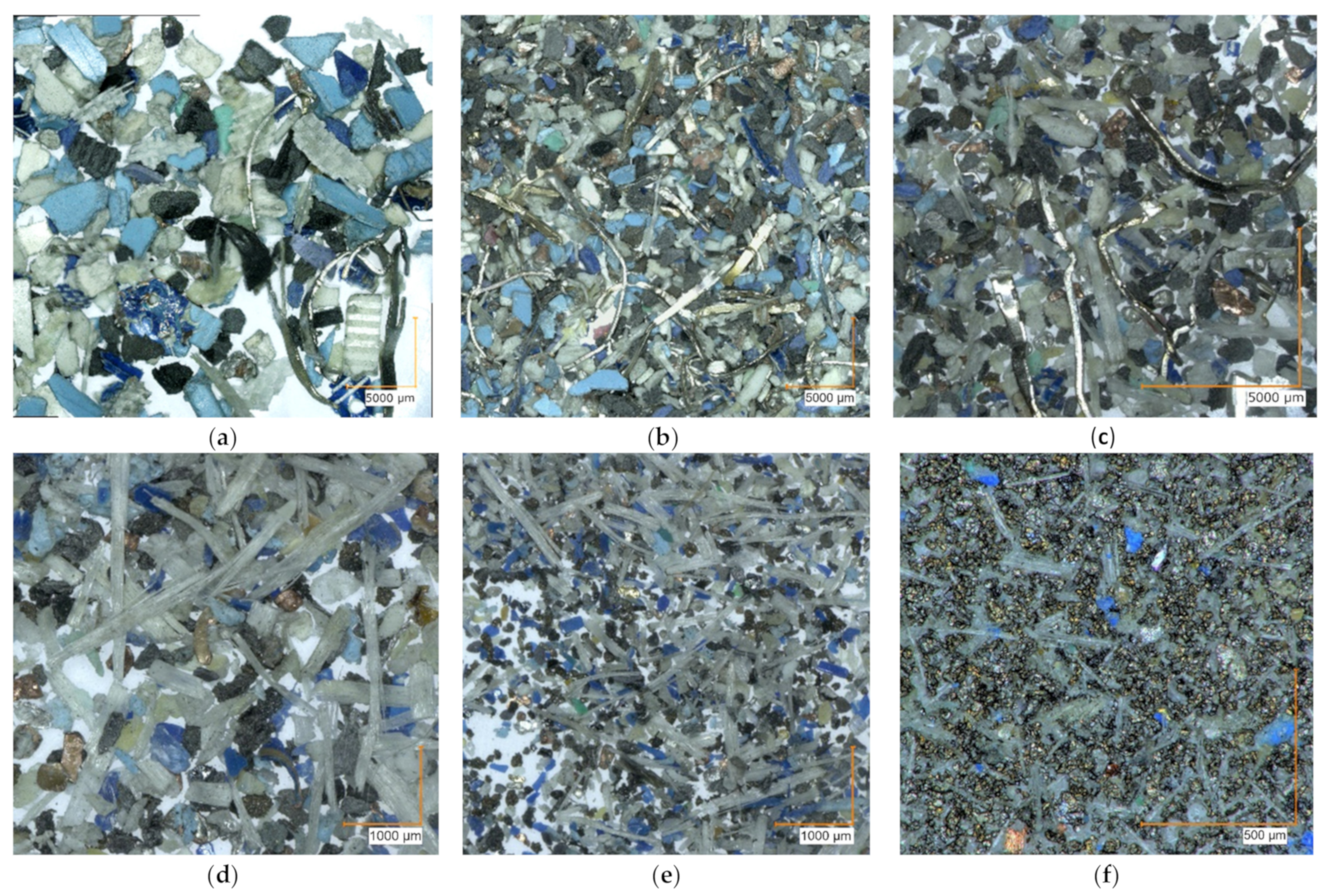
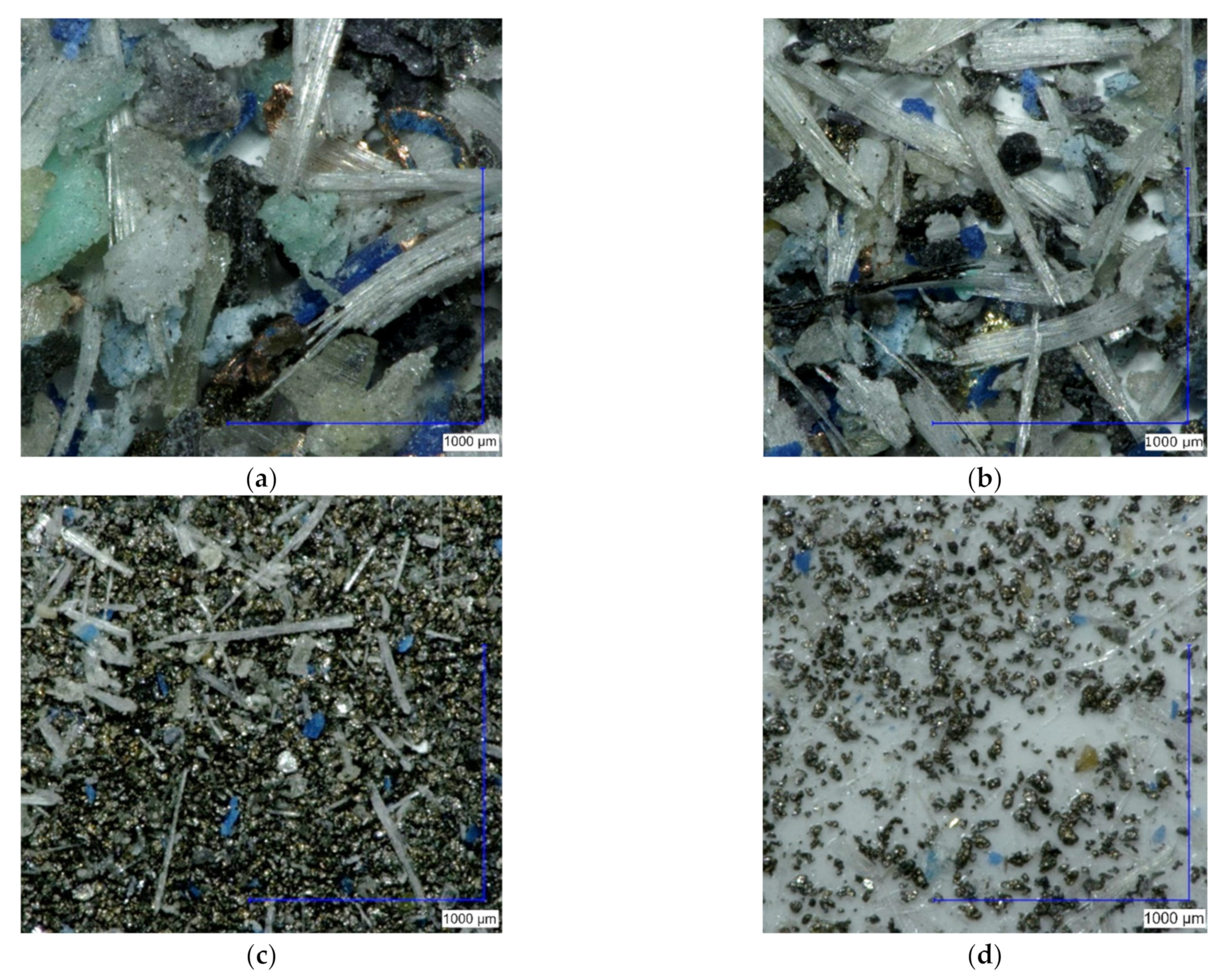
3.2. Morphology and PCBs Disintegration–Milling Dynamics

At the preliminary crushing stage by the disintegration–mill, large pieces of composite PCBs plates quickly disintegrated into parts due to fracture. Then, each separated component is crushed at its achieved linear speed. The morphology of sieved milled particles is represented in Figure 5.
Fractions larger than 2.8 mm were not analyzed in detail and were subjected to secondary milling designated as “X1 (>2.8) + X2”. The fraction with particle sizes from 1.4 to 2.8 mm contained plastic particles (blue, grey, and black color) of equivalent sizes and some wire-like connections, as demonstrated in Figure 5a.
Fractions 0.711–1.40 mm (Figure 5b) and 0.355–0.711 mm (Figure 5c) also contained a significant concentration of plastic particles (blue, grey, and black color). However, the presence of visually observable metallic elements of PCBs was observed to be relatively peeled off from plastic pieces.
Fractions of 0.355–0.18 mm (Figure 5d) and 0.09–0.18 mm (Figure 5e) mainly exhibited fibers from fiberglass elements of PCB components instead of plastic chunks. Remarkably, the smaller the fraction, the lower the concentration of visually observed fibers, indicating the highest fracture resistance to the applied crushing forces inside the disintegration–mill compared to most of the other PCB components.
The X1 finer than 0.09 mm fraction consists primarily of non-plastic components with observable fiberglass, as shown in Figure 5f. Notably, the relatively large fiberglass particles can pass the narrow openings of the sieve mesh by orienting perpendicularly to the surface of the mesh.
Fractions 0.09—0.18 and <0.09 mm of X1 and X1 (>2.8) + X2 disintegration–milled samples visually (Figure 5e,f and Figure 6c,d, respectively) differ by the presence of higher fiber-like plastic particle concentration after one-step milling (X1).
The X1 sample had slightly higher total material amounts in sieved fractions of 2.8–5.6 (5.6 wt.%), 1.4–2.8 (0.1 wt.%), 0.711–1.4 (0.8 wt.%), 0.355–0.711 (3.9 wt.%), and <0.09 mm (0.6 wt.%), as compared to sample X1 (>2.8) + X2 (see Figure 7).
However, slightly higher total material amount in sieved X1 (>2.8) + X2 sample fractions of 0.18–0.35 (0.1 wt.%), 5.6–11.2 (11.1 wt.%), and >11.2 (1.7 wt.%) were measured. It seems more beneficial to perform total metal recovery from disintegration–milled particles with fraction sizes larger than about 1.4 mm. However, the presence of equivalent-sized plastic particles observed in Figure 5a and Figure 6a should be removed prior to the chemical treatment process to reduce the consumption of chemically reactive and avoid harmful emissions by undesirable side reactions.
Glass fibers are poorly reactive to many applied reagents for chemical metal recovery. However, these fibers can be adhered to undesirable side reactions generating polymers. Unfortunately, many metal particles are still attached to plastic and fibrous elements; therefore, the accessibility of chemical reagents to free metals is also limited physically. Therefore, the total metal recovery feasibility of using the largest from disintegration–milled particles should be researched in detail. Particles with sizes under 1.4 mm can be chosen from specimen X1 for economically more feasible total metal recovery compared to the exact particle sizes of X1 (>2.8) + X2, especially in recycling large volumes of PCBs scraps. However, from a common point of view, it is also reasonable to combine these fractions from specimens X1 and X1 (>2.8) + X2. Additional separation based on the density or magnetic properties of the target material could be applied as a next step to remove the separated polymer from disintegration–milled powder and obtain a cleaner product in further studies.
The PCB is a multicomponent metal–plastic multilayer composite material with a complex structure consisting of brittle and plastic components. The mechanisms for reducing the particle size of the plastic and brittle materials are different. The collision of brittle materials with grinding elements results in a natural fracture. However, ductile metallic materials harden during every collision impact. Therefore, the fatigue fracture occurs [42] after two or more have implications inside the disintegration–milling working chamber. These impacts generate a large range of particle size PCBs fractions from <0.009 up to more than 11.2 mm during the one-step milling at 2880 rpm, as demonstrated in Figure 5 and Figure 7.
More advanced disintegration mills have been equipped with separation systems based on aerodynamic force principles. Such systems employ a closed air or gas flow system (so-called inertial classifier) [44]. Such a system can provide ecologically clean disintegration–milling of PCBs into classified powder kinetic energy to give a material transition to collectors without support from additional mechanical transportation and gas blowing devices. Therefore, the required time for sieving into fractions and required energy consumption for plastics, ceramics, and metals separation from target metals by using liquids, gas flows, magnet and electromagnet, isostatic separators, etc., can be significantly reduced.
The performed significant plastic separation from metals with the help of disintegration–milling helps void the incineration stage. The incineration typically leads to highly toxic compounds such as volatile polybrominated dibenzo dioxins and dibenzofurans. Heavy metals can cause secondary pollution (e.g., Pb; see Table 3), and brominated flame retardants leach into groundwater. Therefore, environmentally safe recycling is an important topic for the researcher to satisfy community and local government requirements for greener urban mining.

4. Conclusions

Impact type one-step (X1) disintegration–milling is an effective way to crush PCBs into particles with high MC (from 8.4 to 95.2 wt.% by decreasing particle size fractions from 0.711–1.4 down to <0.09 mm, respectively) before chemical treatment. However, double-step (X1 (>2.8) + X2) treatment leads to a high content of polymers and glass fibers in resulting particle fractions with sizes from <0.09 to 5.6 mm with bulk densities from 2.23 down to 0.30 g·cm−3, respectively. The MC also reduces to 7.2 wt.% (0.711–1.4 mm fraction) and 50.6 wt.% (<0.09 mm fraction), as compared to MC in the same fractions of X1 samples. Many visually observable (by optical microscope) metallic particles still adhere to plastic and fibrous elements after milling. These impurities require additional separation. The presence of polymer particles and fibers has no significant impact on MC compared to the result after the second milling of particles with sizes above 2.8 mm. One-step milling leads to particle fractions with sizes from <0.09 to 2.8 mm with about to six-fold higher bulk densities from 6.8 down to 0.44 g·cm−3, respectively; and up to two-fold higher MC in a finer range of fractions from 0.09 to 0.35 mm, as compared to the result of double-step milling of remaining fractions with particle sizes above 2.8 mm. The approach for the removal of mechanically released particles from metallic elements should be researched in future studies.
Obtained tested particles from PCBs are relatively rich with Fe (up to 867 mg·g−1 in X1, <0.09 mm fraction); Cu (up to 148 mg·g−1 in X1, 0.18–0.35 mm fraction); Sn (up to 51.4 mg·g−1 in X1 (>2.8) + X2, 0.09–0.18 mm fraction); Al (up to 45.2 mg·g−1 in X1 (>2.8) + X2, 0.09–0.18 mm fraction); Ni (up to 14 mg·g−1 in X1, 0.09–0.18 mm fraction); and Zn (up to 10 mg·g−1 in X1, 0.18–0.35 mm fraction). The MC of other metallic elements ranges from about 9 mg·g−1 (Mn in X1, 0.09–0.18 mm fraction) to 0.0006 mg·g−1 (Cd in X1, all tested fractions). The MC of precious elements (Au, Pd, and Pt) are under 0.1 mg·g−1 and require large volumes of PCBs to ensure a profitable metal recovery business. The exception is Ag with MC up to about 1 mg·g−1 (in X1, 0.18–0.35 mm fraction).

Author Contributions

Conceptualization E.B. and A.S. (Andrei Shishkin); methodology V.S.; validation V.P., K.M. and V.Z.; formal analysis A.S. (Andrej Shishko); investigation E.B., A.S. (Andrei Shishkin), D.G. and V.S.; resources, E.B., V.S. and A.S. (Andrei Shishkin); data curation, J.B. and A.S. (Andrei Shishkin); writing—original draft preparation, A.S. (Andrej Shishko) and D.G.; writing—review and editing, J.B.; visualization, A.S. (Andrei Shishkin), A.S. (Andrej Shishko) and J.B.; supervision, A.S. (Andrej Shishko); project administration, E.B.; funding acquisition, E.B. All authors have read and agreed to the published version of the manuscript.

Funding

This research was supported by ERDF project no. 1.1.1.1/20/A/139 “Development of sustainable recycling technology of electronic scrap for precious and non-ferrous metals extraction”. The project was co-financed by REACT-EU funding to mitigate the effects of the pandemic crisis. The article was published with the financial support from the Riga Technical University Research Support Fund. This research was also supported by the Institute of Solid State Physics, University of Latvia as the Center of Excellence has received funding from the European Union’s Horizon 2020 Framework Program H2020-WIDESPREAD-01-2016-2017-TeamingPhase2 under grant agreement No. 739508, project CAMART2.

Data Availability Statement

Not applicable.

Acknowledgments

The authors would also like to mention the support from the “Innovation Grants for Maritime Students” performed at Latvian Maritime Academy (project no: 1.1.1.3/18/A/006, funded by the European Regional Development Fund—ERDF, Republic of Latvia).

Conflicts of Interest

The authors declare no conflict of interest. The funders had no role in the design of the study; in the collection, analyses, or interpretation of data; in the writing of the manuscript; or in the decision to publish the results.

References

  1. Popov, V.V.; Kudryavtseva, E.V.; Kumar Katiyar, N.; Shishkin, A.; Stepanov, S.I.; Goel, S. Industry 4.0 and Digitalisation in Healthcare. Materials 2022, 15, 2140. [Google Scholar] [CrossRef] [PubMed]
  2. Popov, V.V.; Lobanov, M.L.; Stepanov, S.I.; Qi, Y.; Muller-Kamskii, G.; Popova, E.N.; Katz-Demyanetz, A.; Popov, A.A. Texturing and Phase Evolution in Ti-6Al-4V: Effect of Electron Beam Melting Process, Powder Re-Using, and HIP Treatment. Materials 2021, 14, 4473. [Google Scholar] [CrossRef] [PubMed]
  3. Kalisz, S.; Kibort, K.; Mioduska, J.; Lieder, M.; Małachowska, A. Waste Management in the Mining Industry of Metals Ores, Coal, Oil and Natural Gas—A Review. J. Environ. Manag. 2022, 304, 114239. [Google Scholar] [CrossRef]
  4. Toneatti, L.; Deluca, C.; Fraleoni-Morgera, A.; Pozzetto, D. Rationalization and Optimization of Waste Management and Treatment in Modern Cruise Ships. Waste Manag. 2020, 118, 209–218. [Google Scholar] [CrossRef] [PubMed]
  5. Bumanis, G.; Vitola, L.; Stipniece, L.; Locs, J.; Korjakins, A.; Bajare, D. Evaluation of Industrial By-Products as Pozzolans: A Road Map for Use in Concrete Production. Case Stud. Constr. Mater. 2020, 13, e00424. [Google Scholar] [CrossRef]
  6. Sahmenko, G.; Korjakins, A.; Bajare, D. High-Performance Concrete Using Dolomite By-Products. In Concrete Durability and Service Life Planning; Kovler, K., Zhutovsky, S., Spatari, S., M. Jensen, O., Eds.; Springer: Berlin/Heidelberg, Germany, 2020; pp. 99–103. ISBN 978-3-030-43332-1. [Google Scholar]
  7. Lapovok, R.; Popov, V.V.; Qi, Y.; Kosinova, A.; Berner, A.; Xu, C.; Rabkin, E.; Kulagin, R.; Ivanisenko, J.; Baretzky, B.; et al. Architectured Hybrid Conductors: Aluminium with Embedded Copper Helix. Mater. Des. 2020, 187, 108398. [Google Scholar] [CrossRef]
  8. Rumbo, C.; Espina, C.C.; Popov, V.V.; Skokov, K.; Tamayo-Ramos, J.A. Toxicological Evaluation of MnAl Based Permanent Magnets Using Different in Vitro Models. Chemosphere 2021, 263, 128343. [Google Scholar] [CrossRef]
  9. Mori de Oliveira, C.; Bellopede, R.; Tori, A.; Marini, P. Study of Metal Recovery from Printed Circuit Boards by Physical-Mechanical Treatment Processes. Mater. Proc. 2022, 5, 121. [Google Scholar]
  10. Bilesan, M.R.; Makarova, I.; Wickman, B.; Repo, E. Efficient Separation of Precious Metals from Computer Waste Printed Circuit Boards by Hydrocyclone and Dilution-Gravity Methods. J. Clean. Prod. 2021, 286, 125505. [Google Scholar] [CrossRef]
  11. Mandot, V.; Saraswat, V.; Jaitawat, N. Recycling Technologies of PCBs. J. Sci. Approach 2017, 1, 6–11. [Google Scholar] [CrossRef]
  12. Kulu, P.; Goljandin, D. Retreatment of Polymer Wastes by Disintegrator Milling. In Waste Material Recycling in the Circular Economy-Challenges and Developments; Achilias, D.S., Ed.; IntechOpen: Thessaloniki, Greece, 2021; pp. 1–23. ISBN 978-1-83969-681-7. [Google Scholar]
  13. Wen, X.; Zhao, Y.; Duan, C.; Zhou, X.; Jiao, H.; Song, S. Study on Metals Recovery from Discarded Printed Circuit Boards by Physical Methods. In Proceedings of the 2005 IEEE International Symposium on Electronics and the Environment, New Orleans, LA, USA, 16–19 May 2005; pp. 121–128. [Google Scholar]
  14. Wang, H.; Song, X.; Wang, X.; Sun, F. Tribological Performance and Wear Mechanism of Smooth Ultrananocrystalline Diamond Films. J. Mater. Processing Technol. 2021, 290, 116993. [Google Scholar] [CrossRef]
  15. Murugan, R.V.; Bharat, S.; Deshpande, A.P.; Varughese, S.; Haridoss, P. Milling and Separation of the Multi-Component Printed Circuit Board Materials and the Analysis of Elutriation Based on a Single Particle Model. Powder Technol. 2008, 183, 169–176. [Google Scholar] [CrossRef]
  16. Goljandin, D.; Kulu, P. Disintegrators and Disintegrator Treatment of Materials; LAP LAMBERT Academic Publishing: Saarbrücken, Germany, 2015; ISBN 3659647683. [Google Scholar]
  17. Oliveira, P.C.; Taborda, F.C.; Nogueira, C.A.; Margarido, F. The Effect of Shredding and Particle Size in Physical and Chemical Processing of Printed Circuit Boards Waste. Mater. Sci. Forum 2012, 730–732, 653–658. [Google Scholar] [CrossRef]
  18. Kers, J.; Kulu, P.; Goljandin, D.; Kaasik, M.; Ventsel, T.; Vilsaar, K.; Mikli, V. Recycling of Electronic Wastes by Disintegrator Mills and Study of the Separation Technique of Different Materials. Medziagotyra 2008, 14, 296–300. [Google Scholar]
  19. Perdigones, F.; Quero, J. Printed Circuit Boards: The Layers’ Functions for Electronic and Biomedical Engineering. Micromachines 2022, 13, 460. [Google Scholar] [CrossRef]
  20. Chen, Z.; Yang, M.; Shi, Q.; Kuang, X.; Qi, H.J.; Wang, T. Recycling Waste Circuit Board Efficiently and Environmentally Friendly through Small-Molecule Assisted Dissolution. Sci. Rep. 2019, 9, 17902. [Google Scholar] [CrossRef]
  21. Bukhari, M.; Mohd Noor, N.; Nan, N.M.M.; Shamsul, J.B. The Application of PCB, Mounted-Components and Solder Paste in Surface Mount Technology Assembly (SMTA). In Proceedings of the 1st National Conference on Electronic DesignAt: Putra Palace Hotel, Kangar, Malaysia, 18–19 May 2005; pp. 145–151. [Google Scholar]
  22. Khandpur, R.S. Printed Circuit Boards. Design, Fabrication, Assembly, and Testing; Tata McGraw-Hill Education: New York, NY, USA, 2006; ISBN 0070588147. [Google Scholar]
  23. Tilsley, G.M.; Axon, F.J. Comparison of Dry Film and Liquid Photo-Imageable Solder Masks for Surface-Mount Assemblies. Microelectron. Reliab. 1988, 28, 659. [Google Scholar] [CrossRef]
  24. PCBCart PCB Board Material, PCB Material Type. Available online: https://www.pcbcart.com/pcb-capability/pcb-materials.html (accessed on 15 June 2022).
  25. Hino, T.; Agawa, R.; Moriya, Y.; Nishida, M.; Tsugita, Y.; Araki, T. Techniques to Separate Metal from Waste Printed Circuit Boards from Discarded Personal Computers. J. Mater. Cycles Waste Manag. 2009, 11, 42–54. [Google Scholar] [CrossRef]
  26. Paola, M. Recycling of Printed Circuit Boards. In Integrated Waste Management-Volume II; InTech: Houston TX, USA, 2011; ISBN 978-953-307-447-4. [Google Scholar]
  27. Evangelopoulos, P.; Arato, S.; Persson, H.; Kantarelis, E.; Yang, W. Reduction of Brominated Flame Retardants (BFRs) in Plastics from Waste Electrical and Electronic Equipment (WEEE) by Solvent Extraction and the Influence on Their Thermal Decomposition. Waste Manag. 2019, 94, 165–171. [Google Scholar] [CrossRef]
  28. Jonkers, N.; Krop, H.; van Ewijk, H.; Leonards, P.E.G. Life Cycle Assessment of Flame Retardants in an Electronics Application. Int. J. Life Cycle Assess. 2016, 21, 146–161. [Google Scholar] [CrossRef]
  29. Ogunniyi, I.O.; Vermaak, M.K.G.; Groot, D.R. Chemical Composition and Liberation Characterization of Printed Circuit Board Comminution Fines for Beneficiation Investigations. Waste Manag. 2009, 29, 2140–2146. [Google Scholar] [CrossRef]
  30. Ribeiro, P.P.M.; dos Santos, I.D.; Dutra, A.J.B. Copper and Metals Concentration from Printed Circuit Boards Using a Zig-Zag Classifier. J. Mater. Res. Technol. 2019, 8, 513–520. [Google Scholar] [CrossRef]
  31. Huang, T.; Zhu, J.; Huang, X.; Ruan, J.; Xu, Z. Assessment of Precious Metals Positioning in Waste Printed Circuit Boards and the Economic Benefits of Recycling. Waste Manag. 2022, 139, 105–115. [Google Scholar] [CrossRef] [PubMed]
  32. Tatariants, M.; Yousef, S.; Denafas, G.; Bendikiene, R. Separation and Purification of Metal and Fiberglass Extracted from Waste Printed Circuit Boards Using Milling and Dissolution Techniques. Environ. Prog. Sustain. Energy 2018, 37, 2082–2092. [Google Scholar] [CrossRef]
  33. Sousa, P.M.S.; Martelo, L.M.; Marques, A.T.; Bastos, M.; Soares, H. A Closed and Zero-Waste Loop Strategy to Recycle the Main Raw Materials (Gold, Copper and Fiber Glass Layers) Constitutive of Waste Printed Circuit Boards. Chem. Eng. J. 2022, 434, 134604. [Google Scholar] [CrossRef]
  34. Zhou, Y.; Qiu, K. A New Technology for Recycling Materials from Waste Printed Circuit Boards. J. Hazard. Mater. 2010, 175, 823–828. [Google Scholar] [CrossRef]
  35. Arslan, V. Bacterial Leaching of Copper, Zinc, Nickel and Aluminum from Discarded Printed Circuit Boards Using Acidophilic Bacteria. J. Mater. Cycles Waste Manag. 2021, 23, 2005–2015. [Google Scholar] [CrossRef]
  36. Yazici, E.Y.; Deveci, H. Extraction of Metals from Waste Printed Circuit Boards (WPCBs) in H2SO4–CuSO4–NaCl Solutions. Hydrometallurgy 2013, 139, 30–38. [Google Scholar] [CrossRef]
  37. Sahin, M.; Akcil, A.; Erust, C.; Altynbek, S.; Gahan, C.S.; Tuncuk, A. A Potential Alternative for Precious Metal Recovery from E-Waste: Iodine Leaching. Sep. Sci. Technol. 2015, 50, 2587–2595. [Google Scholar] [CrossRef]
  38. Van Yken, J.; Cheng, K.Y.; Boxall, N.J.; Sheedy, C.; Nikoloski, A.N.; Moheimani, N.R.; Kaksonen, A.H. A Comparison of Methods for the Characterisation of Waste-Printed Circuit Boards. Metals 2021, 11, 1935. [Google Scholar] [CrossRef]
  39. Hanafi, J.; Jobiliong, E.; Christiani, A.; Soenarta, D.C.; Kurniawan, J.; Irawan, J. Material Recovery and Characterization of PCB from Electronic Waste. Procedia-Soc. Behav. Sci. 2012, 57, 331–338. [Google Scholar] [CrossRef]
  40. Zimakov, S.; Goljandin, D.; Peetsalu, P.; Kulu, P. Metallic Powders Produced by the Disintegrator Technology. Int. J. Mater. Prod. Technol. 2007, 28, 226. [Google Scholar] [CrossRef]
  41. Peetsalu, P.; Goljandin, D.; Kulu, P.; Mikli, V. Micropowders prozducted by disintegrator milling. Powder Metall. 2003, 3, 99–110. [Google Scholar]
  42. Goljandin, D.; Sarjas, H.; Kulu, P.; Käerdi, H.; Mikli, V. Metal-Matrix Hardmetal/Cermet Reinforced Composite Powders for Thermal Spray. Mater. Sci. 2012, 18, 84–89. [Google Scholar] [CrossRef]
  43. Cui, J.; Zhang, L. Metallurgical Recovery of Metals from Electronic Waste: A Review. J. Hazard. Mater. 2008, 158, 228–256. [Google Scholar] [CrossRef] [PubMed]
  44. Tymanok, A.; Tamm, J.; Roes, A. Flow of Air and Particles Mixture in a Disintegrator. In Proceedings of the Estonian Academy of Sciences, Physics Mathematics, Tallinn, Estonia, 19–20 April 1994; pp. 280–292. [Google Scholar]
Figure 1. As-received computer motherboard (a) and after being cut into pieces before milling (b).
Metals 12 01468 g001
Figure 2. Schematic representation of preliminary size reduction centrifugal-type mill DSL-350. Equipment: 1—rotors; 2—electric drives; 3—material (PCBs) supply; 4—horizontally oriented grinding elements; 5—output.
Metals 12 01468 g002
Figure 3. An applied disintegration–milling, sieving, and testing scheme show an approach for selecting fractions of powders from PCBs for metal content determination after one-step (X1) and double-step (X1 (>2.8) + X2) disintegration–milling.
Metals 12 01468 g003
Figure 4. Dependence of element composition of milled fraction by particle size distribution for X1 (one-step) (a) and X1 (>2.8) + X2 (double-step for >2.5 mm fractions from first milling) (b) millings.
Metals 12 01468 g004
Figure 5. Optical images of the fractions 1.4–2.8 mm (a), 0.711–1.4 mm (b), 0.355–0.711 mm (c), 0.355–0.18 mm (d), 0.09–0.18 mm (e) and <0.09 mm with significantly lower fiberglass concentration (f) after one-step milling (X1).
Metals 12 01468 g005
Figure 6. Optical images of the fractions 0.711–1.4 mm (a); 0.355–0.711 mm (b); 0.09–0.18 mm (c); and <0.09 mm (d) after double-step milling (X1 (>2.8) + X2) of fraction >2.8 mm collected from the one-step milling.
Metals 12 01468 g006
Figure 7. Particle size distribution of the disintegration–milled PCBs after first “X1” and second milling of the fraction with particle sizes larger than 2.8 mm from first milling designated as “X1 (>2.8) + X2”.
Metals 12 01468 g007
Table 1. Typical PCB composition attributed to the general groups of materials, data from [30].
Metals
(~40 wt.% in Total)
wt.%
of Metals
Ceramics
(~30 wt.% in Total)
wt.%
of Ceramics
Plastics
(~30 wt.% in Total)
wt.%
of Plastics
Cu6–27SiO215–30Polyethylene10–16
Fe1.2–8Al2O36–9.4Polypropylene4.8
Al2–7.2Alkali-earth oxides6Polystyrene4.8
Sn1–5.6Titanates-micas3Epoxy resin4.8
Pb1–4.2 Polyvinyl chloride2.4
Ni0.3–5.4 Polytetrafluoroethylene2.4
Zn0.2–2.2 Nylon0.9
Sb0.1–0.4
Au (ppm)250–2050
Ag (ppm)110–4500
Pd (ppm)50–4000
Pt (ppm)5–30
Co (ppm)1–4000
Table 2. Characteristics of the high-energy disintegration–mill DSL-350.
ParameterValue
Type of device (position of rotors)horizontal
Grinding environmentair
Rotor systemone/two-rotor
Number of pins/blades roads1/3
Rotation velocity of rotors, rpm2880
Impact velocity, m/sup to 180
Specific energy of treatment ES, kJ·kg−1up to 13.6
Possible operating systemdirect
Input (max particle size), mm45
Productivity, kg·h−1up to 950
Table 3. Bulk densities and MC of one-step (X1) and double-step (X1 (>2.8) + X2) milled PCB fractions.
Fraction, mm<0.090.09–0.180.18–0.350.35–0.7110.711–1.41.4–2.82.8–5.6
Bulk density of X1, g·cm−36.85.34.91.60.440.610.30
Bulk density of X1 (>2.8) + X2, g·cm−32.230.840.810.530.580.35
MC in X1, wt.%95.2 ± 1.857.7 ± 1.554.6 ± 1.214.3 ± 0.98.4 ± 0.5
MC in X1 (>2.8) + X2, wt.%50.6 ± 1.326.2 ± 1.633 ± 0.98 ± 0.77.2 ± 0.6
Table 4. MC changes (in %) from double (X1 (>2.8) + X2) to one-step (X1) milling PCB by fractions.
Metal Content in % after One-Step Milling in Comparison with Double-Step MillingTotal MC *
Fraction, mmAgAuPdPtAlCdCoCrCuFeMnMoNiPbSbSnTiVZn
0.18–0.3586400140025676886121003798552794514432981006346
0.09–0.1841160010010044678131177015485624547100303576470119
<0.09121130087058767720745982640577731545124
Notes: * Total extracted MC by fraction. Green color (positive value) exhibits the benefit (higher metal content) of one-step milling in comparison with double-step milling approach. Yellow color (zero value) exhibits no effect of double-step milling in comparison to one-step milling. Red color (negative value) exhibits the benefit of double-step milling in comparison with one-step milling.
Publisher’s Note: MDPI stays neutral with regard to jurisdictional claims in published maps and institutional affiliations.

