Article

Obtainment of Residual Stress Distribution from Surface Deformation under Continuity Constraints for Thinned Silicon Wafers

1
School of Mechanical Engineering, Hefei University of Technology, Hefei 230009, China
2
Anhui Engineering Laboratory of Intelligent CNC Technology and Equipment, Hefei 230009, China
3
Collaborative Innovation Center of Suzhou Nano Science and Technology, Soochow University, Suzhou 215021, China
*
Authors to whom correspondence should be addressed.
Machines 2021, 9(11), 284; https://doi.org/10.3390/machines9110284
Submission received: 29 September 2021 / Revised: 29 October 2021 / Accepted: 8 November 2021 / Published: 11 November 2021
(This article belongs to the Section Material Processing Technology)

Abstract

:
Precision machining (e.g., fine grinding, polishing) induced residual stress is very small and often not constant across the wafer and it is difficult to be directly obtained by stress testing equipment or Stoney equation. The residual stress could be obtained theoretically based on the principle of superposition in which the entire wafer deformation is taken as the sum of all deformations induced by the residual stresses of different positions on the wafer surface. However, the solved residual stress is affected greatly by deformation measurement errors and fluctuates greatly across the wafer surface. To solve the problem, a regularization method with continuity constraints was proposed in this study. The mechanisms for the discontinuity of the residual stress distribution and the sensitivity of calculation results to the measurement errors were studied. The influences of the number of subareas of the silicon wafer were investigated and the continuity constraint term was constructed based on the positional relationship of different subareas. Stable and continuous residual stress distribution was successfully obtained after using the proposed regularization method. The method may also be applied to estimate the residual stress from surface deformation for thin substrate plates of other materials.

1. Introduction

With the lithographic line width reaching the physical limit, integrated circuit chips are shifting from transistor scaling to three-dimension integration [1,2]. Silicon wafer thinning is needed to satisfy the demand for three-dimension integrated circuits packaging since the primary wafer thickness is relatively large to retain enough stiffness [3,4]. Grinding is the commonly used technique to remove redundant material for its high efficiency [5]. Chemo-mechanical polishing is subsequently conducted to eliminate subsurface damage introduced in the grinding process and improve the reliability of final chips [6].
The subsurface damage introduced in precision machining is often evaluated by destructive methods. The silicon wafers are diced and the microscopic morphology of the cross-section is observed by scanning electron microscopes (SEM) or transmission electron microscopes (TEM) to evaluate the processing quality [7,8]. Gao et al. compared the subsurface damage images machined by grinding with those of chemo-mechanical polishing [9]. The nature of the cross-section observation methods is to acquire the information of the microstructure changes of monocrystalline silicon. However, the subsurface damage is not uniformly distributed on the surface in the microscale due to the mechanical properties of anisotropic single crystal silicon, which restricts the repeatability improvement of the methods. Raman spectroscopy is also a common method for the evaluation of processing quality [10,11,12]. Like the aforementioned methods, the frequency shift of Raman microscopes corresponds to the microstructure changes, and the measured values will fluctuate evidently when the sampling positions change. Besides, the resolution of Raman spectroscopy is limited and cannot be applied when the subsurface damage introduced in the precision machining process is very small.
In the precision machining (e.g., fine grinding, polishing), the residual stress is generated when there exists plastic deformation in the subsurface damage layer. There is a definite correspondence between the residual stress and the subsurface damage for a specific manufacturing process. Therefore, the residual stress of thinned silicon wafers is preferred to be known as it is an important indicator of the subsurface damage and is very useful in the study of precision machining mechanisms. The residual stress leads to the wafer deformation and there is a definite correspondence between them. The residual stress could be obtained inversely from the wafer deformation data [13]. Stoney equation is often used to relate the residual stress to the geometric parameters of the wafer deformation [14,15]. However, the residual stress and the deformation curvature are assumed to be constant across the silicon wafer, which is often contrary to the actual scenarios of thinned silicon wafers [16].
The authors have engaged in research on the deformation measurement of silicon wafers and found that the deformation of thinned silicon wafers could be obtained accurately after eliminating the effect of gravity [17,18]. Unlike the cross-section observation methods which are focused on the microstructure changes, the deformations of silicon wafers are the overall effects of all the residual stresses across the wafer surface and show the potential for the evaluation of processing quality. Stoney equation cannot be applied when the residual stress or the wafer deformation curvature is not constant across wafer surfaces. However, if the silicon wafer is divided into many subareas each subarea is small enough that the residual stress in one subarea would be approximately the same. Then the residual stress could be obtained based on the principle of superposition in which the entire wafer deformation is calculated as the sum of residual stress-induced deformation of all subareas [19]. However, there exists a multi-collinearity problem and small measurement errors would lead to large changes in residual stress calculation results. Besides, the residual stress distribution is not continuous across the wafer surface, which does not agree with actual situations [13]. The conventional regularization method using an Identify matrix as the Tikhonov matrix was used in our previous research. The overfitting phenomenon was improved and the calculated largest residual stress value was reduced [18]. However, the continuity problem of the residual stress distribution across the wafer was not directly addressed since the positional relationship of different subareas was not taken into consideration.
In this study, the mechanisms for the discontinuity of the residual stress distribution across the wafer and the sensitivity of calculation results to the measurement errors were explored. The influences of the number of subareas and the number of elements in one subarea were investigated. Finally, a regularization method considering continuity constraints in the residual stress calculation process was proposed. The residual stress calculation results with continuity constraints were compared with those without continuity constraints to verify the effectiveness of the proposed method.

2. Principle of Residual Stress Obtainment

When the silicon wafer is divided into small subareas the residual stress could be assumed to be uniformly distributed in one subarea when the division number is large enough. The wafer deformation caused solely by the unit stress load of one subarea could be obtained by finite element simulation and the total wafer deformation is the sum of the wafer deformations caused by residual stresses of all subareas and a system of linear equations could be obtained based on their relationship. For each linear equation, the total wafer deformation at a certain point is equal to the sum of the wafer deformations at the same point caused by residual stresses of all subareas. Then, the actual residual stresses of divided subareas could be obtained by solving the equations.
A number of n points were used to characterize the wafer deformation. The value of the ith point for the total wafer deformation was denoted as ti. The wafer was divided into m subareas. The deformation value of the ith point was denoted as Aij in which j corresponded to the jth subarea under the unit load. For the jth subarea, if the actual residual stress is σj the wafer deformation at the ith point would be Aijxj. xj is the coefficient of proportionality between the actual residual stress and the unit load for the jth subarea and could be expressed as follows:
x j = σ j σ u
The total wafer deformation at the ith point ti was the sum of wafer deformations at the same point caused by residual stresses of all divided subareas based on the principle of linear superposition. Their relationship could be expressed as:
A i 1 x 1 + A i 2 x 2 + A i 3 x 3 + + A i m x m = t i
There were n linear equations corresponding to the n points and there were m variables to be determined in the system of linear equations. The system of linear equations could be transformed into a matrix equation [13], which is shown in Equation (3).
A x = t
where
A = ( A 11 A 12 A 1 m A 21 A 22 A 2 m A 31 A 32 A 3 m A n 1 A n 2 A n m ) x = ( x 1 x 2 x m ) t = ( t 1 t 2 t 3 t n )
The variable x could be obtained as the least-squares solution [20], as shown below.
x = (ATA)–1 ATt
In Equation (5), t is the measured wafer deformation value. The deformation of a double-sided polished silicon wafer was obtained by the three-point-support method based on the position determination of supports and wafers [
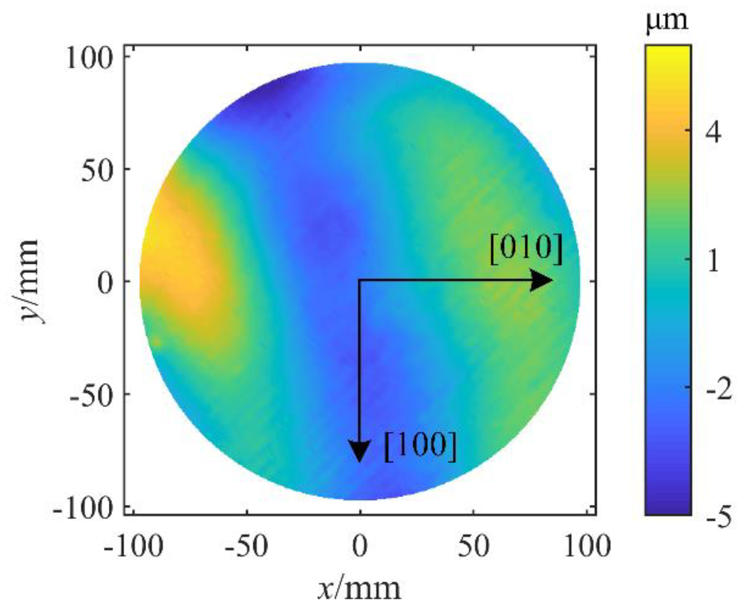
17], which is shown in Figure 1. The diameter of the silicon wafer was 200 mm and the thickness was 333 μm. The columns of A were acquired using finite element models and the vector x could be obtained by solving Equation (5).
One column of matrix 
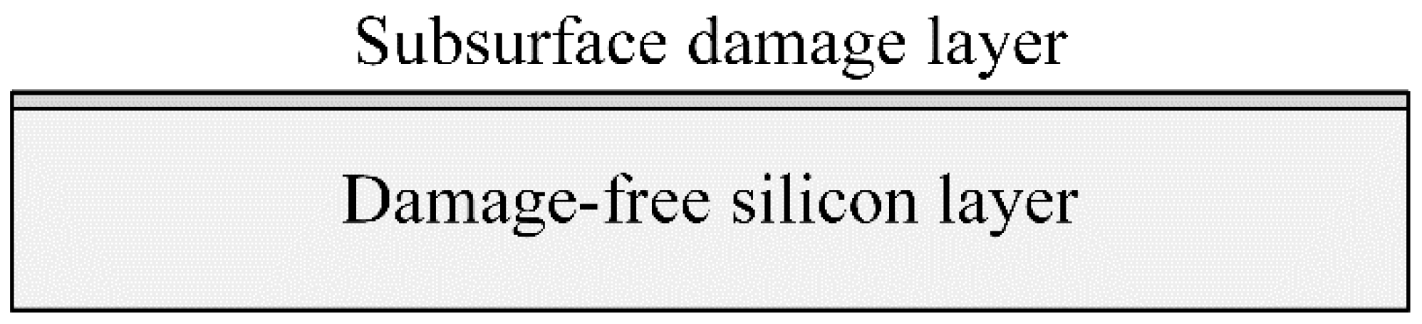
A corresponded to the wafer deformation with one subarea applied a unit load of residual stress. The finite element model was established using commercially available software (Ansys 15.0, Ansys Inc., Canonsburg, USA). The silicon wafer consisted of two layers, as shown in Figure 2. One layer was the damage-free silicon wafer with perfect lattice and there was no residual stress in the layer. On top of the damage-free silicon layer was the subsurface damage layer. There might exist residual stresses on both sides of the silicon wafer. However, the wafer deformation caused by compressive residual stress on one side equals to be that caused by tensile residual stress of the same size on the other side [14]. Therefore, it could be simplified and the residual stress in the subsurface damage layer in Figure 2 represented the residual stresses of both sides. The details of the finite element model of silicon wafers could be found in our previous study [18].
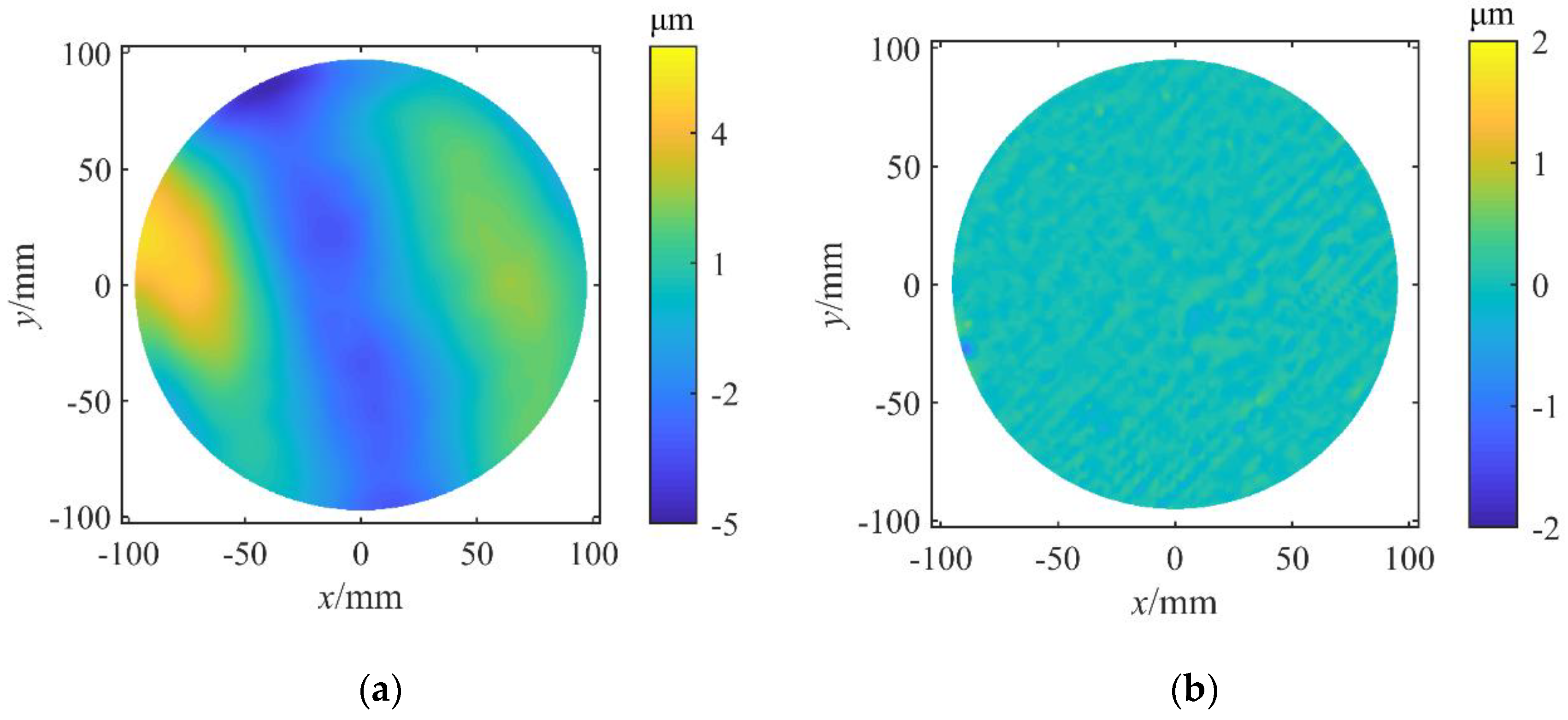
The total wafer deformation was simulated using the calculated 
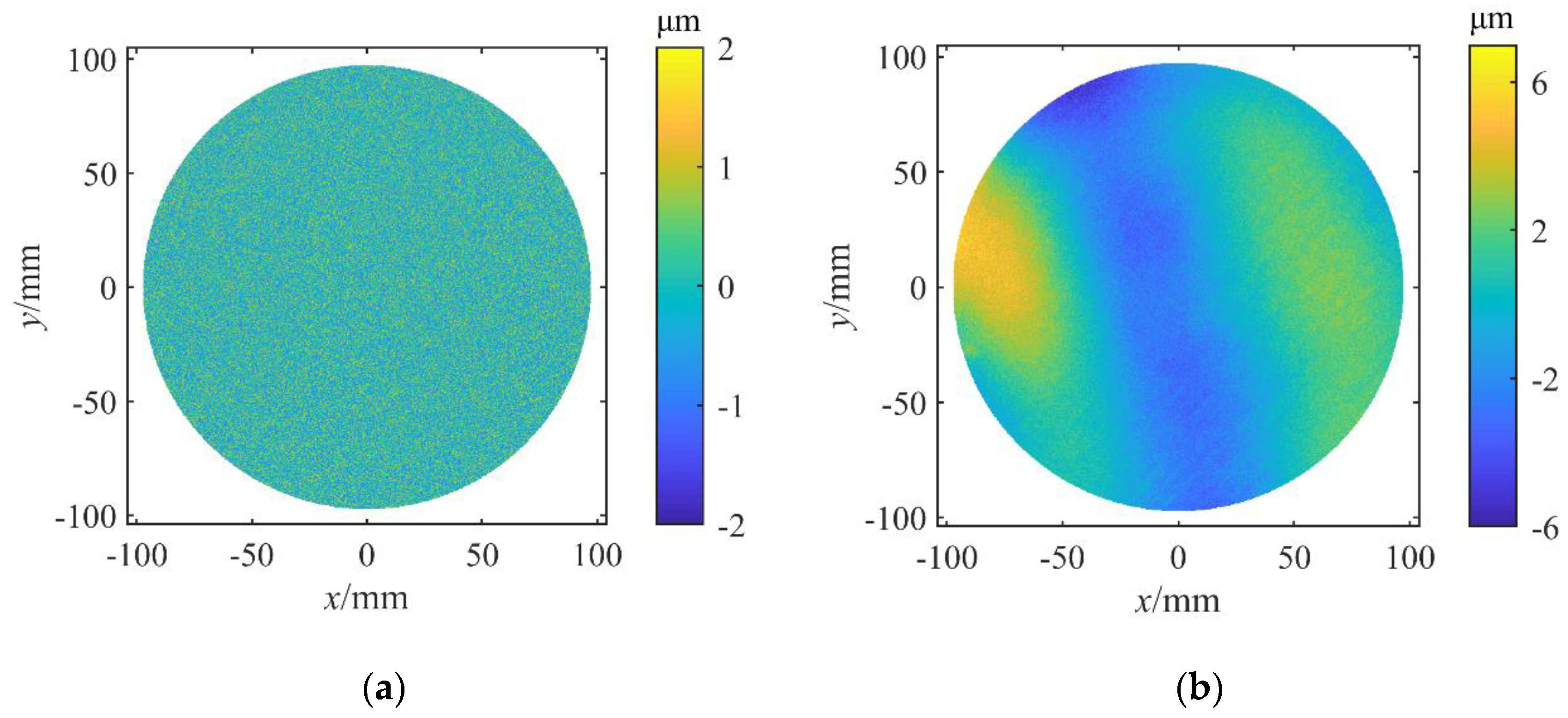
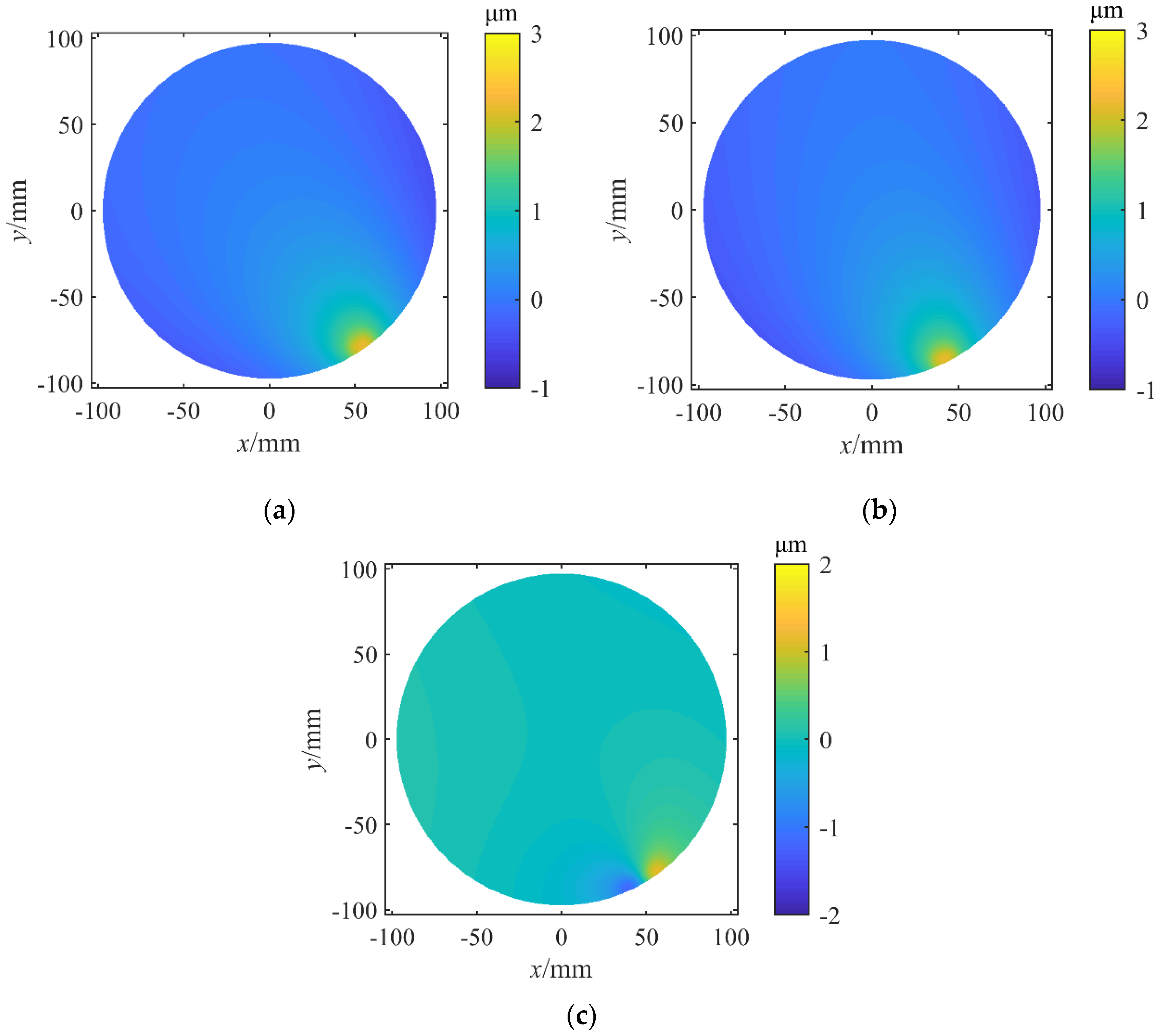
x and compared with the measurement result to verify the method. As shown in Figure 3, the simulated wafer deformation was almost identical to the measurement result (Figure 1). In most regions the difference was smaller than 1 μm, indicating that the calculated residual stress distribution could reproduce the desired wafer deformation.
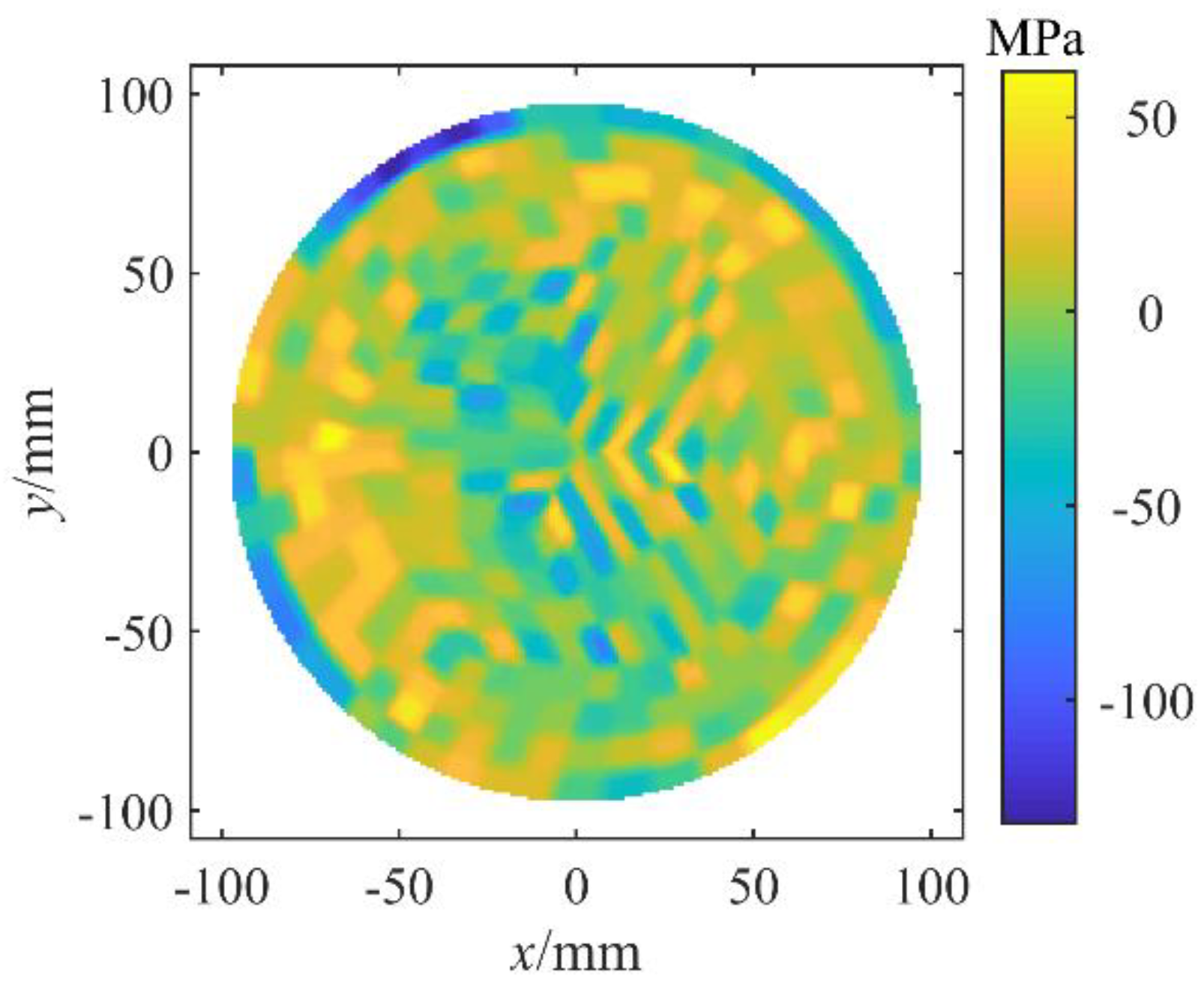
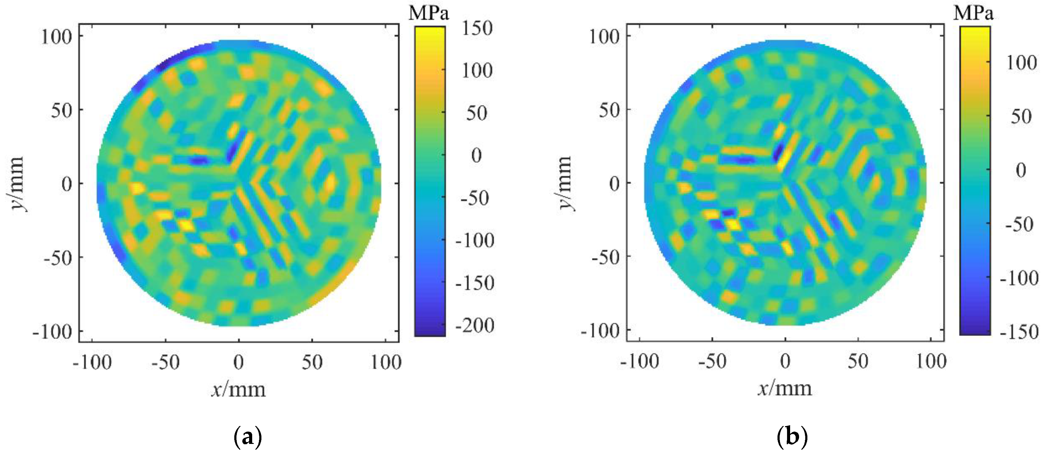
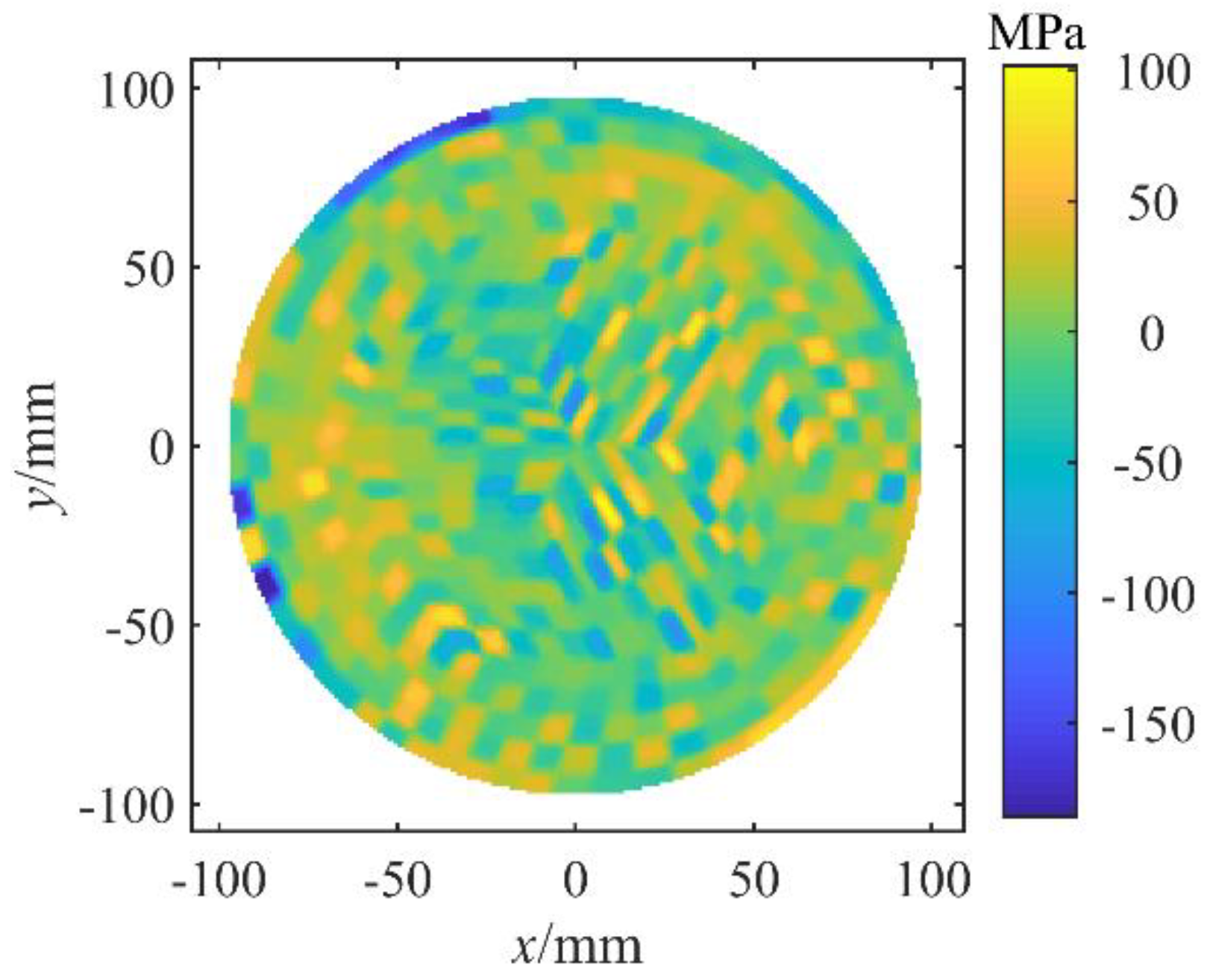
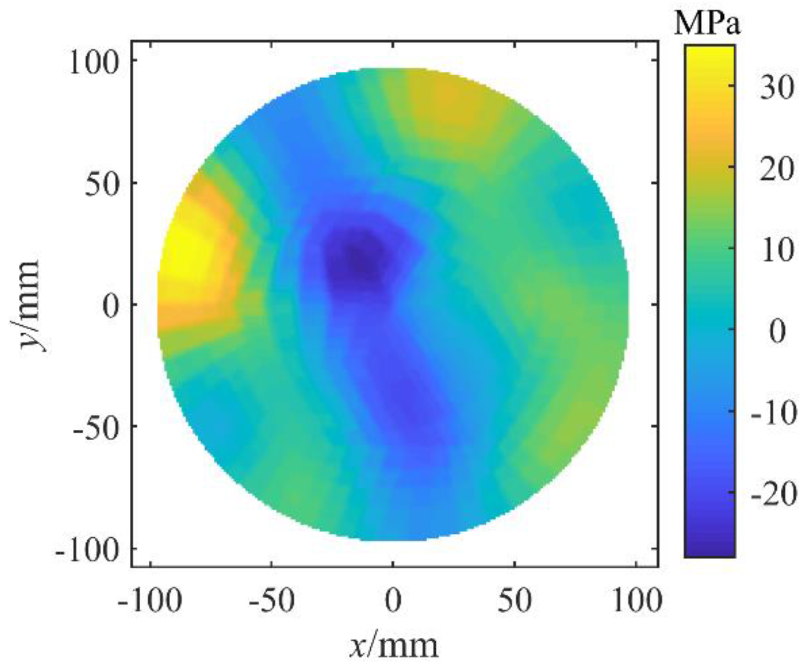
The residual stress distribution calculated using Equation (5) was plotted in Figure 4. It was found that the residual stresses of adjacent subareas changed significantly across the wafer surface, which was contrary to the character of the polishing process. In the polishing process, the surface of the polishing pad was smooth and the density of abrasive grain trajectories was uniformly distributed along the wafer surface. Therefore, the residual stress obtained from wafer deformation by solving Equation (5) which was adopted in reference [13] was not true and new methods needed to be explored to obtain reasonable solutions.

3. Effects of Model Settings

3.1. Effect of Condition Number of Matrix A

In Equation (5), the difficulty with the solution of the least-squares problem was that the matrix A was ill-conditioned. Its condition number was very large, which implied that the computed solution was potentially very sensitive to perturbations of the measured deformation values. To evaluate the influence of the condition number of matrix A, random errors were added to the original measured deformation data and the residual stress distribution was recalculated to see the changes. The random errors were generated in the numerical range of −1 μm to 1 μm, which was reasonable compared with the magnitude of measurement errors [17]. The generated random error distribution is shown in Figure 5a and the silicon wafer deformation after adding the errors is shown in Figure 5b. The added random errors led to the noisy points in Figure 5b but the deformation feature was unchanged. For a robust computation method, the solution of the residual stress distribution should be stable.
The recalculated residual stress distribution and its difference from Figure 4 are shown in Figure 6. It was found that the residual stress changed significantly although the change of the wafer deformation was very limited. The largest difference value reached over 150 MPa·μm, which was contrary to actual scenarios that similar wafer deformations should have similar stress distributions.
The reason behind the changes should be that the condition number of A was very large. When the condition number cond2(A) was large, the smallest nonzero eigenvalue of ATA was very small, indicating the matrix was very close to being singular. The closer the matrix was to be singular, the more ill-conditioned it was, meaning the solution was very sensitive to perturbations of the data t.

3.2. Effect of Number of Elements in One Subarea

The condition for Equation (5) to be solved was that the number of sampling points n was equal or greater than the number of subareas m. Therefore, on average at least one point in one subarea should be sampled. Besides, the columns of matrix A should be linearly independent of each other to obtain the unique solution without free variables, meaning the sampling points in one subarea should be independent of each other. However, the number of divided elements in one subarea would affect the solution accuracy and might be linked to the linear correlation of different columns of matrix A.
The number of divided elements in one subarea was changed to see its effect on the condition number of matrix A. One extreme case was that there was only one element in one subarea, meaning the unit residual stress was applied to one element for each simulation. For example, the silicon wafer was divided into 336 elements and the deformation values of 4218 sampling points were exported to construct matrix A. It was found that the condition number was over one million, indicating that the columns of matrix A were very close to linear correlation. The reason was that the deformation values of points in one element were obtained by interpolation using the shape function in the finite element model and were not completely independent of each other.
The number of divided elements in one subarea was increased to 4, 9, 16, 25, and 36 to see its effect. The condition number changes were shown in Figure 7 and it was found that the condition number stabilized after the number of divided elements exceeded 25, which meant the density of meshing of the subarea was sufficient. Therefore, the number of divided elements in one subarea was set to 36 in the following simulations.

3.3. Effect of Number of Subareas

The finite element model would be more accurate with the increase in the number of subareas. More divided subareas mean that one subarea is smaller and the model is closer to actual situations. However, it was found that the condition number of matrix A would increase evidently with the increase of the number of subareas, as shown in Figure 8. A large condition number would cause the problem to be more ill-conditioned. As discussed before, the large condition number cond2(A) means that the matrix is close to being singular, indicating that the columns of A are nearly linearly dependent. The reason was explored by investigating the difference between wafer deformations under unit stress loads applied on two adjacent subareas.
As shown in Figure 9, the wafer deformation under unit load on one subarea presented the feature that the region with relatively large deformation values coincided with the subarea where the residual stress was applied. For adjacent subareas, their wafer deformation features resembled each other and the difference was plotted in Figure 9c. In most regions of the silicon wafer, the difference was smaller than 1 μm, meaning the two columns of matrix A were very close to each other and nearly linear dependent.
When the number of subareas increased from 336 to 525 the size of one subarea became smaller since the total wafer size was constant. As shown in Figure 10, the wafer deformation values turned smaller, leading to a smaller difference between wafer deformations for adjacent subareas. The largest difference value turned to be 0.8 μm, which was much smaller than that in Figure 9c. Therefore, the two columns of matrix A were closer to each other and more linearly dependent when the number of subareas increased.
The residual stress calculation result was shown in Figure 11. Due to the increase of condition number of matrix A there existed large fluctuations of residual stress values between adjacent subareas. Compared with the residual stress distribution in Figure 4, both the largest compressive and tensile residual stress values increased evidently.
The difference of residual stress values between adjacent subareas should be smaller when the subareas became smaller. However, the calculation result of residual stress distribution presented large differences in residual stress values between adjacent subareas due to the similarities of columns of matrix A. Therefore, a regularization method with continuity constraints was needed to solve Equation (5) so that the calculated residual stress results could simultaneously satisfy deformation conformity and continuity of residual stress distribution across the silicon wafer.

4. Regularization Method with Continuity Constraints

The solution of variable x using Equation (5) is the direct solution of the inverse problem. The solution errors have a mean of zero, are uncorrelated, and have equal variances. The calculated results of residual stress are the best linear unbiased estimator of the coefficients, which is known as the Gauss–Markov theorem [21]. It means that the solution of variable x would enable the wafer deformation calculated by Ax to be the closest approximation to the measured result t, which could be expressed as:
min x A x t 2
However, the relationships of xj (j = 0, 1, …, m) were assumed to be independent of each other during the solution process, which was incompatible with the actual situations. Therefore, the solution fluctuated greatly when small perturbations were introduced to the measurement result t. Regularization methods could be adopted to obtain numerically stable solutions in which additional information is integrated to solve the ill-posed problem [22]. In this study, the continuity constraint was constructed to obtain the stable solution of variable x.
Tikhonov regularization method is the most commonly used regularization method [23]. The method is to obtain the solution x which minimizes the following weighted sum:
min x { A x t 2 + μ L x 2 }
where μ was the trade-off parameter, L was the Tikhonov matrix. The parameter of μ was used to control the weight given to the minimization of the constraint. In this study, the Tikhonov matrix L was constructed to add the continuity constraint, which was expressed as follows:
L = ( L 11 L 12 L 1 m L 21 L 22 L 2 m L 31 L 32 L 3 m L m 1 L m 2 L m m )
The main diagonal elements of the matrix L were all set to 8 which equaled the number of closest subareas to be selected, the other elements were set to −1 or 0. For each subarea, the centroid x and y location values were recorded. The distance between the centers of any two subareas was calculated. For each subarea, the other subareas were sorted by the distance values from this subarea. Eight subareas with the smallest distance values were recorded and the corresponding matrix element in L was set to −1. The number of recorded closest subareas could also be selected as other values depending on the number of subareas.
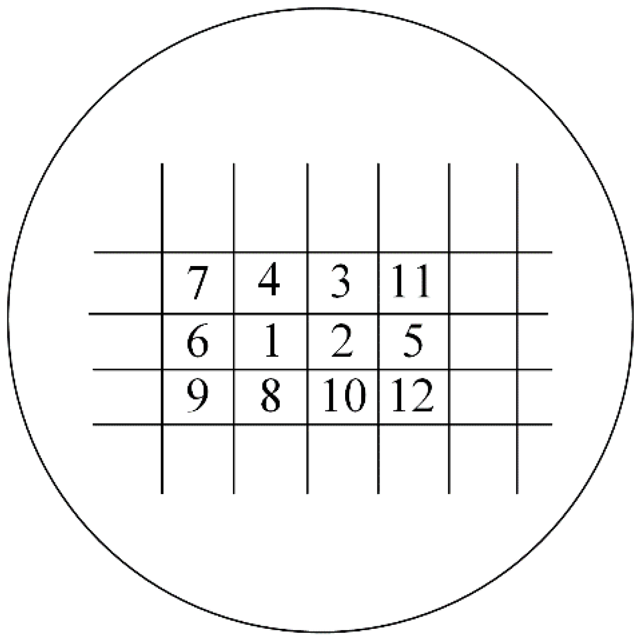
For example, there were m subareas numbered from 1 to m. For the first subarea, the eight closest to it were Subarea 2, Subarea 3, Subarea 4, Subarea 6, Subarea 7, Subarea 8, Subarea 9, and Subarea 10 in Figure 12. Then the first row of matrix L should be (8, −1, −1, −1, 0, −1, −1, −1, −1, −1, 0, 0, …, 0). For the second subarea, the eight closest to it were Subarea 1, Subarea 3, Subarea 4, Subarea 5, Subarea 8, Subarea 10, Subarea 11, and Subarea 12. Then the second row of matrix L should be (−1, 8, −1, −1, −1, 0, 0, −1, 0, −1, −1, −1, …, 0).
Therefore, the matrix L should be expressed as:
L = ( 8 1 1 1 0 1 1 1 1 1 0 0 0 1 8 1 1 1 0 0 1 0 1 1 1 0 L m 1 L m 2 L m 3 L m 4 L m 5 L m 6 L m 7 L m 8 L m 9 L m 10 L m 11 L m 12 8 )
The other rows of matrix L could be obtained using the same method. Then the Lx could be expressed as:
L x = ( 8 x 1 x 2 x 3 x 4 x 6 x 7 x 8 x 9 x 10 8 x 2 x 1 x 3 x 4 x 5 x 8 x 10 x 11 x 12 8 x m + L m 1 x 1 + L m 2 x 2 + + L m ( m 1 ) x m 1 )
The Euclidean norm of Lx could be expressed as:
L x 2 = ( ( 8 x 1 x 2 x 3 x 4 x 6 x 7 x 8 x 9 x 10 ) 2 + ( 8 x 2 x 1 x 3 x 4 x 5 x 8 x 10 x 11 x 12 ) 2 + + ( 8 x m + L m 1 x 1 + L m 2 x 2 + + L m ( m 1 ) x m 1 ) 2 ) 1 / 2
It could be inferred from Equation (11) that the Euclidean norm of Lx would be smaller with the decrease of the difference of residual stresses between adjacent subareas. An extreme case was that the residual stress values were all the same across the wafer surface. In the case, x1, x2, x3,…, and xn were all equal to each other and the terms (8x1x2x3x4x6x7x8x9x10)2, (8x2x1x3x4x5x8x10x11x12)2, …, and (8xm + Lm1x1 + Lm2x2 + Lm3x3 + … + Lm(m−1)xm−1)2 were all zeros. Then the value of the ‖Lx2 would be zero.
When the matrix L was determined, the variable x could be calculated from the following equation:
x = (ATA + μL)–1 ATt
The parameter μ was chosen based on the balance between the value of ‖Axt2 and that of ‖Lx2. The term ‖Axt2 was adopted to evaluate the misfit of the solution x which was the measure of data fidelity. When the value of ‖Axt2 was very large, the difference between the simulated and the measured wafer deformation was large, indicating the underfitting of the solution. The term ‖Lx2 was used to evaluate the continuity of solution x. When the value of ‖Lx2 was very large, the changes of residual stresses of adjacent subareas were large. Different μ values were chosen to calculate the corresponding values of ‖Axt2 and ‖Lx2. Then the plot of residual norm ‖Axt2 of the regularized solution versus the corresponding norm of ‖Lx2 could be obtained, which was called the trade-off curve, as shown in
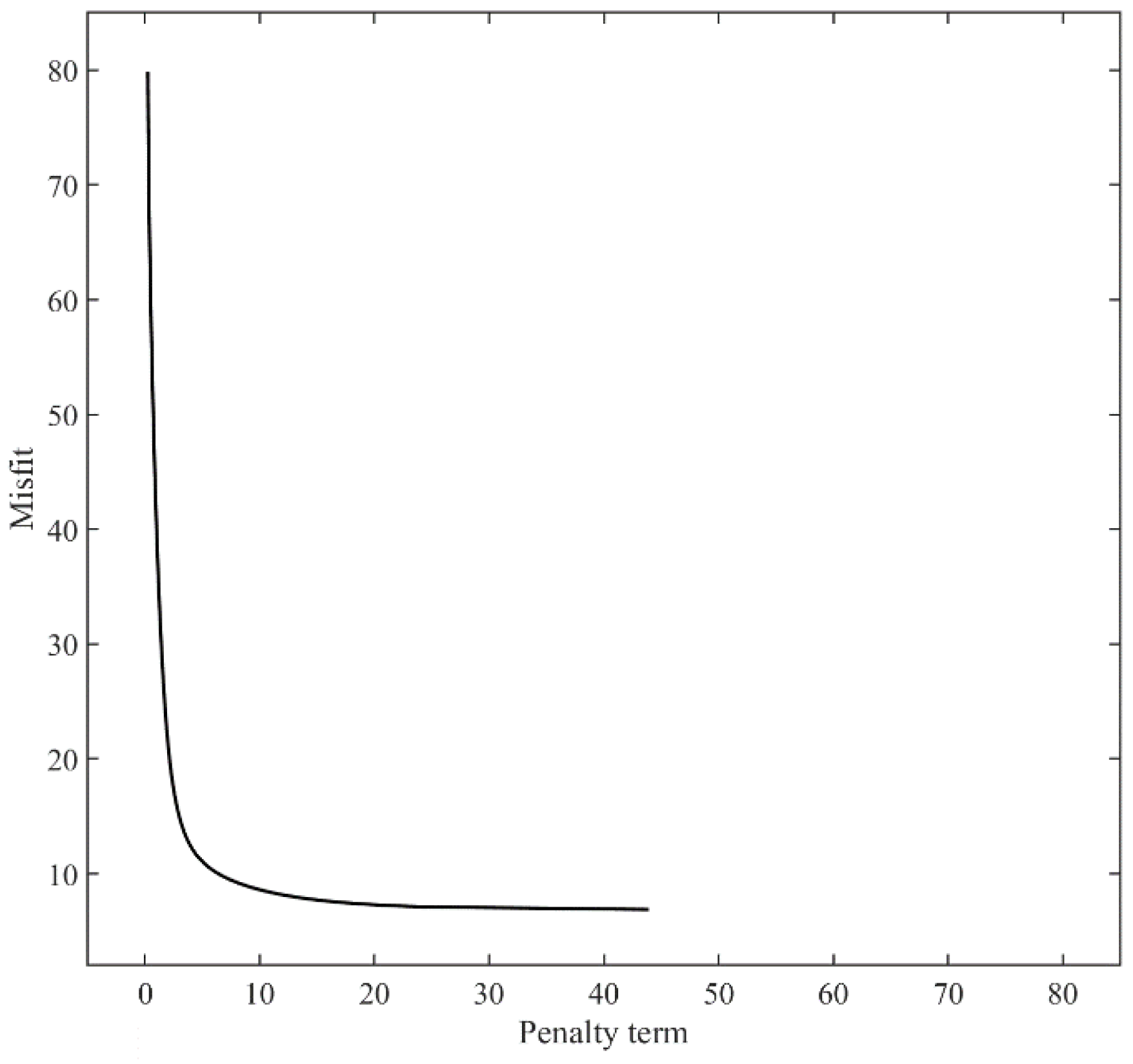
 Figure 13.
The vertical part of the trade-off curve corresponded to x values where the simulated wafer deformation differed a lot from the measured wafer deformation. In contrast, the horizontal part of the trad-off curve corresponded to x values where there existed large discontinuities in the residual stress distribution. Therefore, the value of μ was chosen in the corner region.
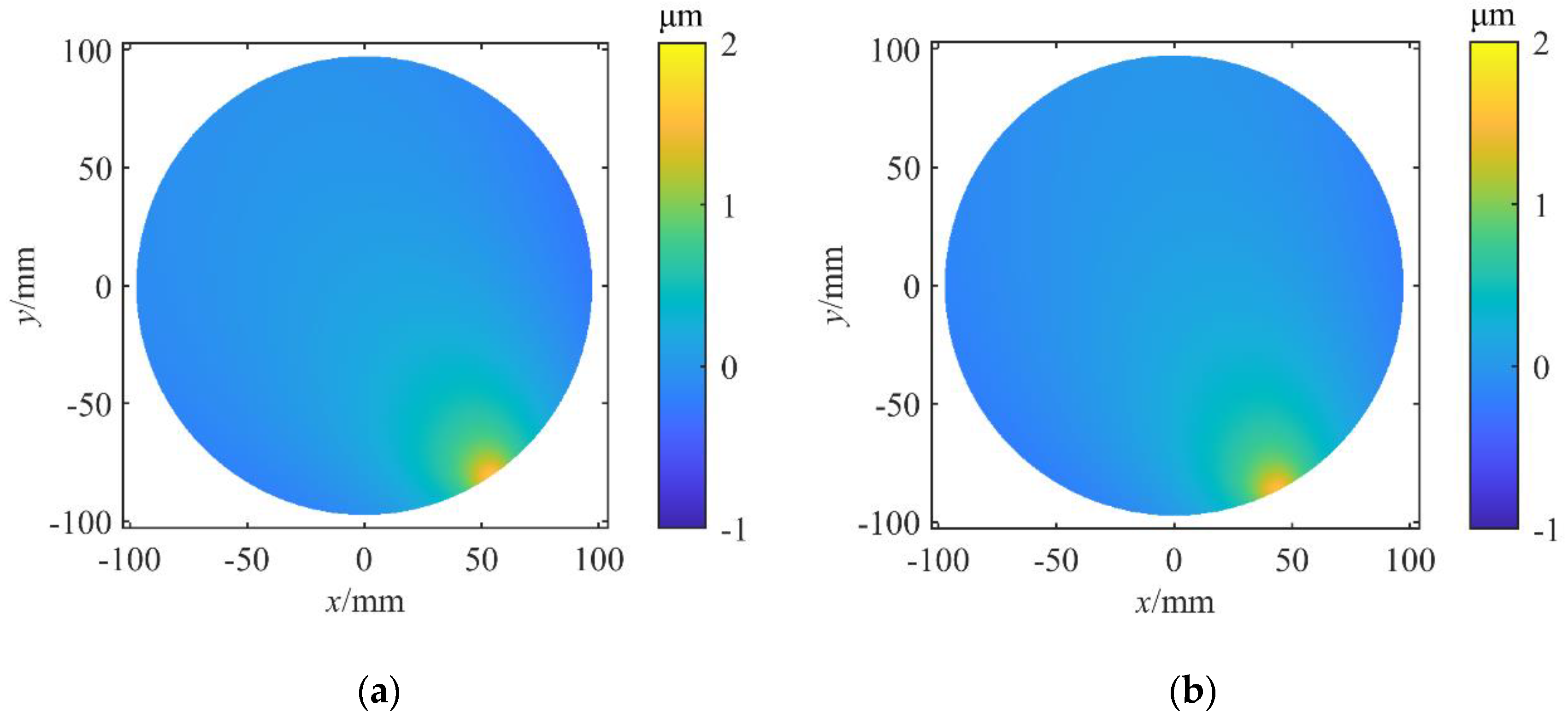
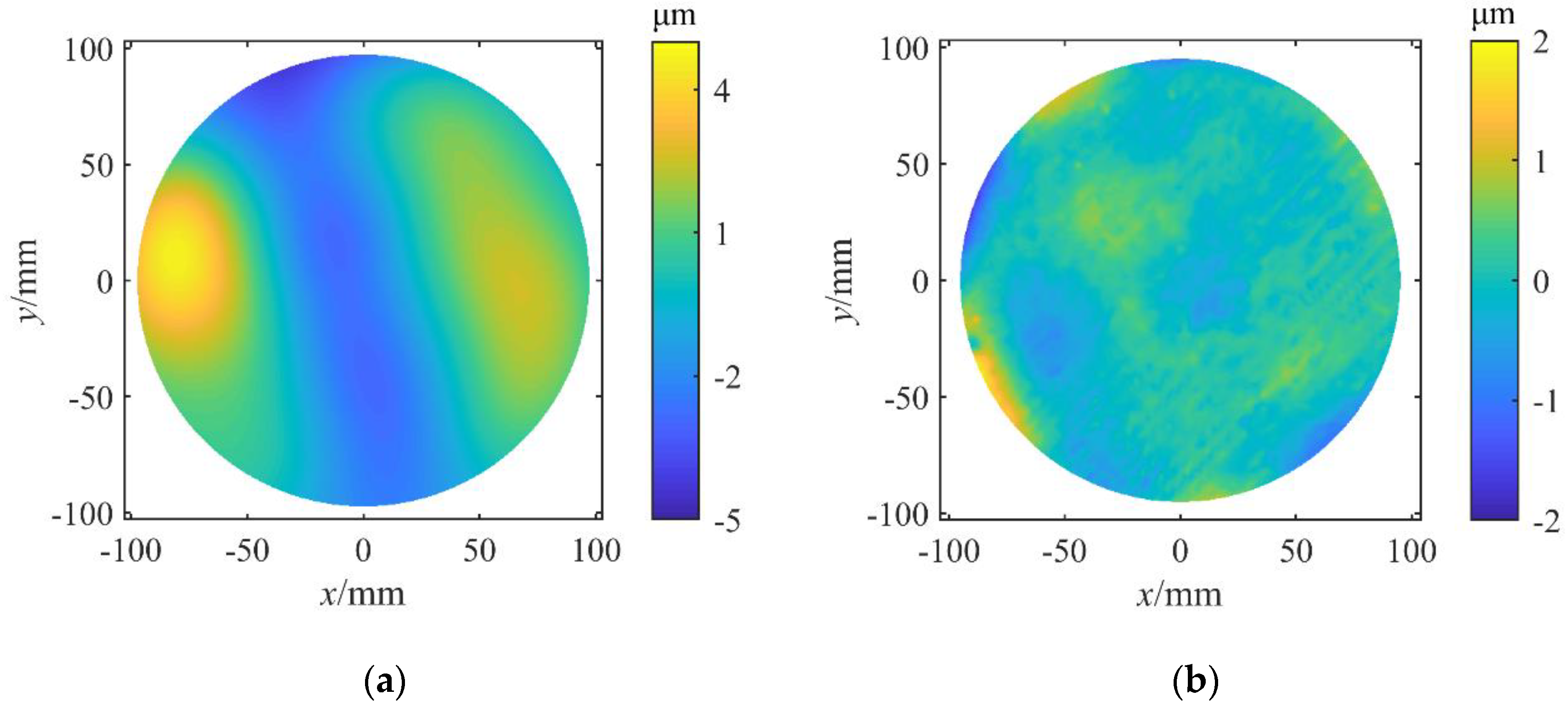
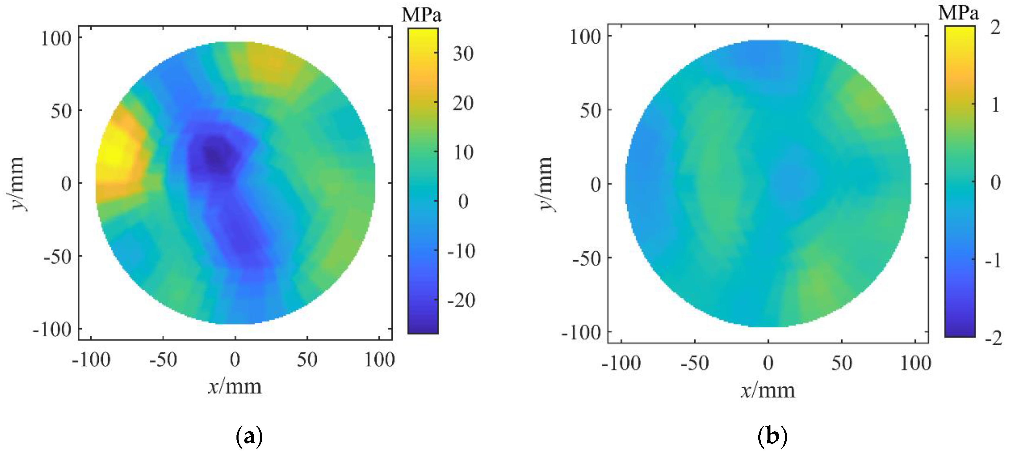
When the parameter μ was determined, the variable x was obtained using Equation (12). The difference between the simulated and the measured wafer deformation was checked if it was within the allowable range. As shown in Figure 14, the simulated wafer deformation still reproduced the morphological characteristics of the measurement results. The difference in distribution is shown in Figure 14b. The absolute deviation values of about 90% of the points are less than 0.5 μm. About 9% of the total points are over 0.5 μm but less than 1 μm. Only about 1% of the total points are over 1 μm but still less than 2 μm, which means that the calculated deformation fits well with the measured deformation considering the measurement uncertainty of the wafer deformation [17]. It should be noted that the greatest deviation seems to be more likely to appear on the edge of the wafer since edge roll-off would occur in the polishing process and the error of measured deformation in vicinity of the wafer edge would be a little larger.
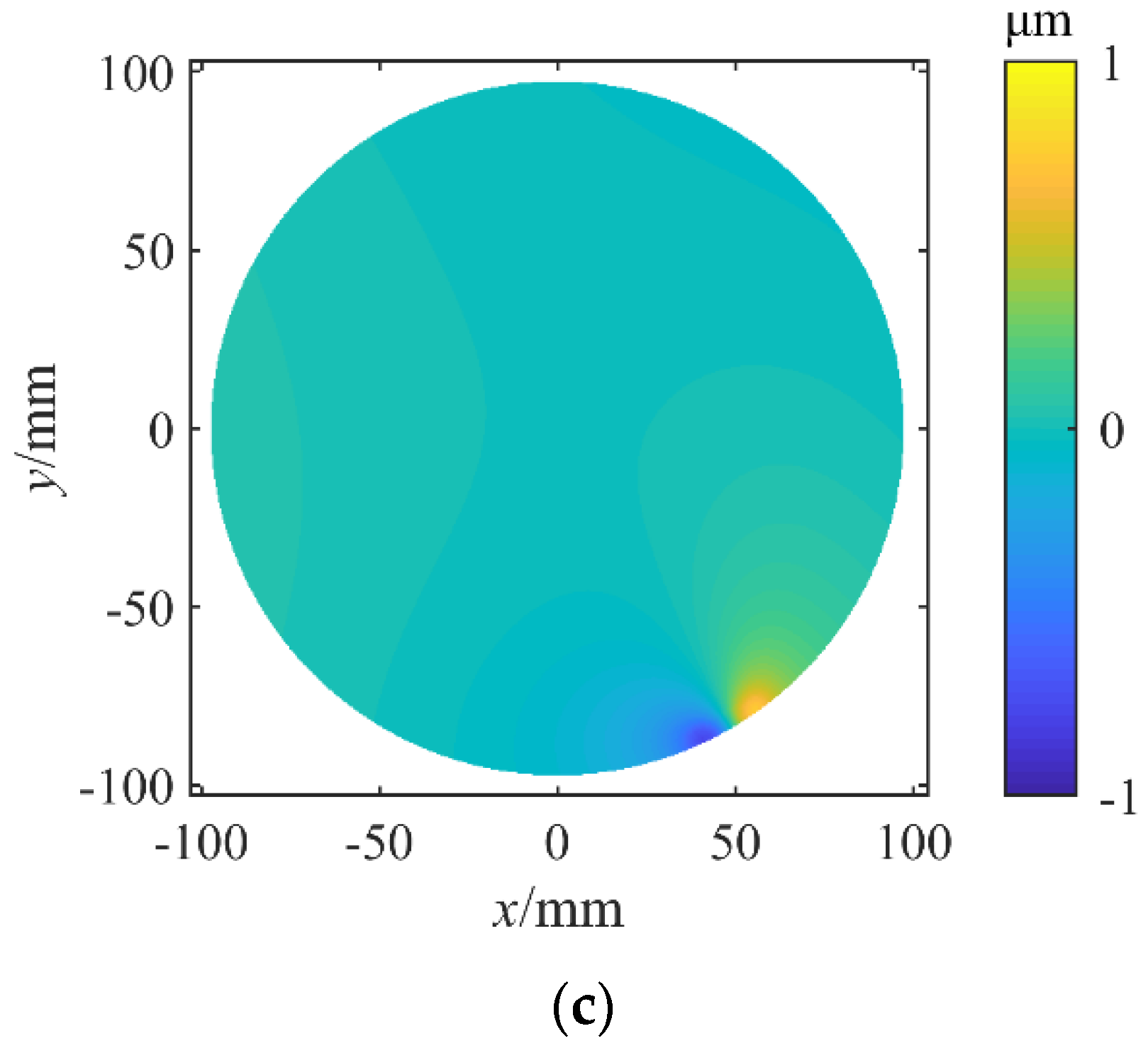
Compared with the results in Figure 3 without using the regularization method, the difference was a little larger but the extent was very limited. That was because the solution x was not an unbiased estimator anymore after introducing the term ‖Lx2 in Equation (7). The introduction of regularization methods reduced the variance at the cost of introducing a tolerable amount of bias. As shown in 
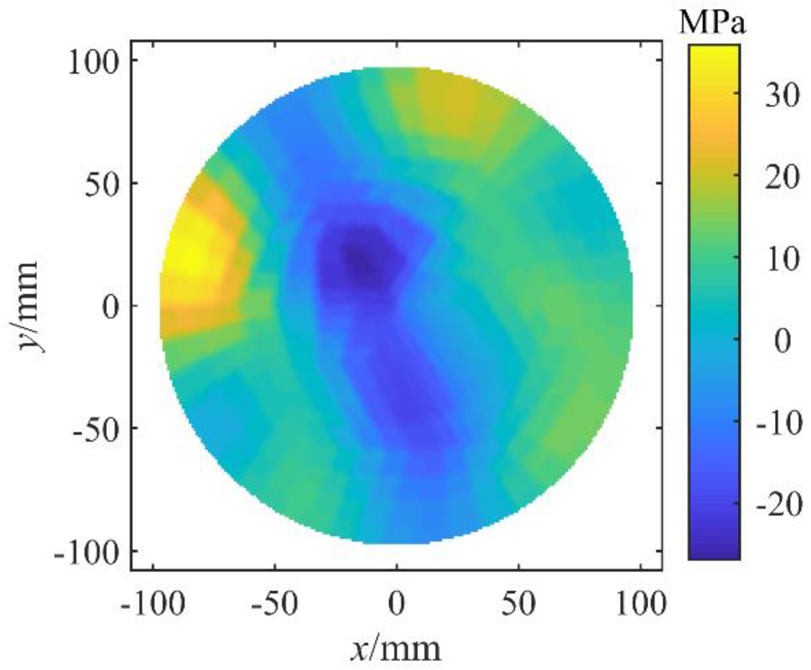
Figure 15, the calculated residual stress distribution presented the feature of being continuous between adjacent subareas. Besides, the solution turned to be more robust to measurement errors. The residual stress distribution was recalculated from the wafer deformation (Figure 5b) with random errors, which was shown in Figure 16. It was found that the change of the solution x was very limited, proving the validity of the regularization method.
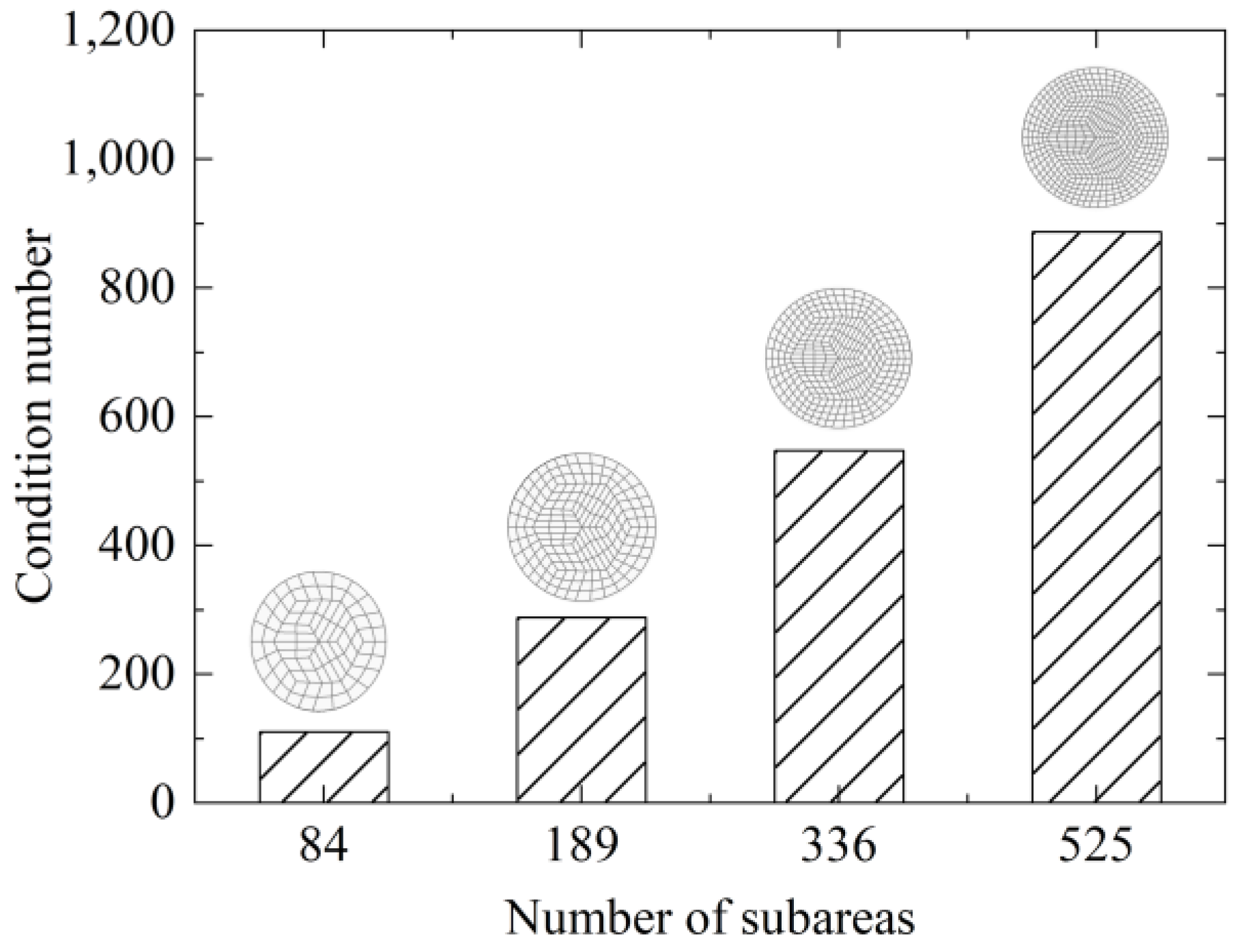
The residual stress was also calculated using the regularization method when the division number was 525 (Figure 17). The characteristic of the residual stress distribution was almost the same as that when the division number was 336 (
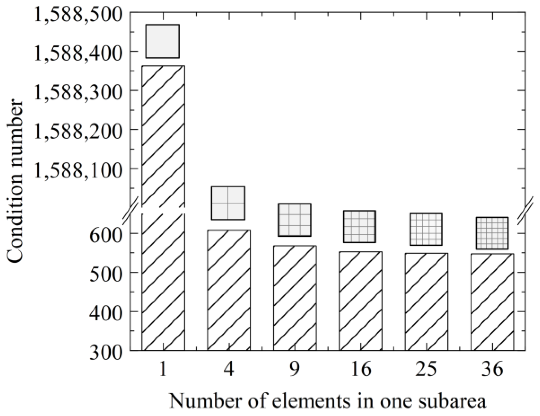
Figure 15), which indicated that the regularized method with continuity constraints was robust to the number of subareas of the wafer. A larger number of subareas was preferred since it was closer to the actual situation but it would increase the computational workload to get the solution. When the increase of the number of subareas does not improve the solution evidently, it means that the differentiation of the wafer surface is enough to character the true status of residual stress distribution.
The Tikhonov matrix L could also be an Identify matrix I to improve the solution result [18]. However, the effect of the positional relationship between different xis is neglected and the improvement of the continuity of the residual stress distribution across the wafer is limited. Besides, the imposing of the side constraint Ix tends to lead to smaller residual stress values than the actual scenarios since the constraint term ‖Ix2 equals to be the Euclidean norm of vector x. The absolute values of xis tend to be smaller to minimize the term μx2 of the total sum when using an Identify matrix I as the Tikhonov matrix, especially when the trade-off parameter μ is large. One extreme case is that xis would be all zeros when the parameter μ is infinitely great to minimize the sum of ‖Axt2 and μx2. The calculated xis using the proposed method in this study could maintain its original accuracy for various wafers since the value of the ‖Lx2 has no direct correlation with the absolute residual stress values.

5. Conclusions

There is a definite correspondence between residual stress and wafer deformation and the residual stress could be obtained from the wafer deformation theoretically. However, the wafer deformations caused by unit residual stress loads of adjacent subareas were very similar to each other. Small measurement errors led to significant changes in residual stress calculation results due to the multicollinearity problem and the residual stresses distribution fluctuated greatly across the wafer surface. The effect of the number of divided elements in one subarea was limited. But the condition number of the coefficient matrix turned larger and the accuracy of the solution further deteriorated with the increase of the number of subareas, which restricted the refinement of the model.
The regularization method with continuity constraints was proposed in this study. The Tikhonov matrix L was constructed based on the positional relationship of different subareas and the continuity constraint ‖Lx2 was added to the minimization objective function. The trade-off parameter μ was chosen based on the balance between the misfit value of ‖Axt2 and the continuity constraint value of ‖Lx2. The continuity of the residual stress distribution was improved significantly using the regularization method. Besides, the calculated xis using the proposed method in this study could maintain its original accuracy for various wafers while smaller xis tend to be obtained when using an Identify matrix I as the Tikhonov matrix.
The residual stress could be obtained using the proposed regularization method with continuity constraints by the wafer deformation and used to assess the machining process independent of the wafer geometric dimension. Its change before and after a machining process could help monitor the process-induced residual stress and optimize the processing parameters. This method could also be applied to other large and thin substrate plates.

6. Patents

The work reported in this manuscript has been applied for an invention patent (Patent No. CN202110358535.6).

Author Contributions

Conceptualization, H.L.; writing—original draft, H.L.; funding acquisition, H.L.; software, T.Y.; writing—review and editing, T.Y., X.T., S.C. and L.L.; resources, J.H.; project administration, L.L. All authors have read and agreed to the published version of the manuscript.

Funding

This research was funded by National Natural Science Foundation of China, grant number 51805135.

Institutional Review Board Statement

Not applicable.

Informed Consent Statement

Not applicable.

Data Availability Statement

Not applicable.

Conflicts of Interest

The authors declare no conflict of interest.

References

  1. Schmitt, R.P.; Menk, L.A.; Baca, E.; Bower, J.E.; Romero, J.A.; Jordan, M.B.; Jackson, N.; Hollowell, A.E. Void-free Copper Electrodeposition in High Aspect Ratio, Full Wafer Thickness Through-Silicon Vias with Endpoint Detection. J. Electrochem. Soc. 2021, 167, 162517. [Google Scholar] [CrossRef]
  2. Shen, W.; Chen, K. Three-Dimensional Integrated Circuit (3D IC) Key Technology: Through-Silicon Via (TSV). Nanoscale Res. Lett. 2017, 12, 56. [Google Scholar] [CrossRef] [PubMed] [Green Version]
  3. Zhang, X.; Yang, C.; Zhang, Y.; Hu, A.; Li, M.; Gao, L.; Ling, H.; Hang, T. Sub-surface Damage of Ultra-Thin Monocrystalline Silicon Wafer Induced by Dry Polishing. Electron. Mater. Lett. 2020, 16, 355–362. [Google Scholar] [CrossRef]
  4. Liu, Y.; Chu, Y.; Tu, K.N. Scaling effect of interfacial reaction on intermetallic compound formation in Sn/Cu pillar down to 1 μm diameter. Acta Mater. 2016, 117, 146–152. [Google Scholar] [CrossRef]
  5. Zhou, P.; Yan, Y.; Huang, N.; Wang, Z.; Kang, R.; Guo, D. Residual Stress Distribution in Silicon Wafers Machined by Rotational Grinding. J. Manuf. Sci. Eng. 2017, 139, 081012. [Google Scholar] [CrossRef]
  6. Satake, U.; Matsui, S.; Enomoto, T. Polishing pad for reducing edge roll-off while maintaining good global flatness of silicon wafer. Precis. Eng. 2020, 66, 577–592. [Google Scholar] [CrossRef]
  7. Yan, D.; Qin, F.; Sun, J.; Wang, Z.; Tang, L. Subsurface Damage Distribution of Ground Silicon Wafers. In Proceedings of the 15th International Conference on Electronic Packaging Technology, Chengdu, China, 12–15 August 2014; IEEE: New York, NY, USA, 2014; pp. 871–873. [Google Scholar]
  8. Inoue, F.; Jourdain, A.; Peng, L.; Phommahaxay, A.; De Vos, J.; Rebibis, K.J.; Miller, A.; Sleeckx, E.; Beyne, E.; Uedono, A. Influence of Si wafer thinning processes on (sub)surface defects. Appl. Surf. Sci. 2017, 404, 82–87. [Google Scholar] [CrossRef]
  9. Gao, S.; Huang, H.; Zhu, X.L.; Kang, R.K. Surface integrity and removal mechanism of silicon wafers in chemo-mechanical grinding using a newly developed soft abrasive grinding wheel. Mater. Sci. Semicond. Process. 2017, 63, 97–106. [Google Scholar] [CrossRef]
  10. Chen, L.; Zhang, X.; Zhang, T.; Liu, H.Y.; Lee, S. Micro-Raman Spectral Analysis of the Subsurface Damage Layer in Machined Silicon Wafers. J. Mater. Res. 2000, 15, 1441–1444. [Google Scholar] [CrossRef]
  11. Yan, J.; Asami, T.; Harada, H.; Kuriyagawa, T. Crystallographic effect on subsurface damage formation in silicon microcutting. CIRP Ann.-Manuf. Technol. 2012, 61, 131–134. [Google Scholar] [CrossRef]
  12. Yan, J.; Asami, T.; Kuriyagawa, T. Nondestructive measurement of machining-induced amorphous layers in single-crystal silicon by laser micro-Raman spectroscopy. Precis. Eng. 2008, 32, 186–195. [Google Scholar] [CrossRef]
  13. Obata, Y.; Yoneyama, S. Inversion of Residual Stresses in Silicon Wafer from Surface Deflection Measurements. In Residual Stress, Thermomechanics & Infrared Imaging and Inverse Problems; Springer: Cham, Switzerland, 2020; pp. 75–81. [Google Scholar]
  14. Janssen, G.C.A.M.; Abdalla, M.M.; van Keulen, F.; Pujada, B.R.; van Venrooy, B. Celebrating the 100th anniversary of the Stoney equation for film stress: Developments from polycrystalline steel strips to single crystal silicon wafers. Thin Solid Film. 2009, 517, 1858–1867. [Google Scholar] [CrossRef]
  15. Stoney, G.G. The tension of metallic films deposited by electrolysis. Proc. R. Soc. Lond. A 1909, 82, 172–175. [Google Scholar]
  16. Finot, M.; Blech, I.A.; Suresh, S.; Fujimoto, H. Large deformation and geometric instability of substrates with thin-film deposits. J. Appl. Phys. 1997, 81, 3457–3464. [Google Scholar] [CrossRef]
  17. Liu, H.; Zhu, X.; Kang, R.; Dong, Z.; Chen, X. Three-point-support method based on position determination of supports and wafers to eliminate gravity-induced deflection of wafers. Precis. Eng. 2016, 46, 339–348. [Google Scholar] [CrossRef]
  18. Liu, H.; Zhou, J.; Han, J.; Tian, X.; Chen, S.; Lu, L. Evaluation of polishing-induced subsurface damage based on residual stress distribution via measured global surface deformation for thinned silicon wafers. Surf. Topogr. Metrol. Prop. 2021, 9, 035001. [Google Scholar] [CrossRef]
  19. Yoneyama, S.; Arikawa, S. Identification of Boundary Condition from Measured Displacements for Linear Elastic Deformation Fields. Procedia IUTA 2012, 4, 215–226. [Google Scholar] [CrossRef] [Green Version]
  20. Schomaker, M.; Rao, C.R.; Toutenburg, H.; Heumann, C. Linear Models and Generalizations: Least Squares and Alternatives; Springer Science & Business Media: Berlin/Heidelberg, Germany, 2007. [Google Scholar]
  21. Hallin, M. Gauss–Markov Theorem in Statistics. In Wiley StatsRef: Statistics Reference Online; John Wiley & Sons, Ltd.: Hoboken, NJ, USA, 2014. [Google Scholar]
  22. Hansen, P.C. Regularization Tools version 4.0 for Matlab 7.3. Numer. Algorithms 2007, 46, 189–194. [Google Scholar] [CrossRef]
  23. Liskovets, O.A. Theory and the methods of solution of ill-posed problems. J. Sov. Math. 1986, 34, 1656–1696. [Google Scholar] [CrossRef]
Figure 1. Measured surface deformation of a double-sided polished silicon wafer.
Machines 09 00284 g001
Figure 2. Two layers of the silicon wafer in the finite element model.
Machines 09 00284 g002
Figure 3. Simulated wafer deformation (a) and the difference from measured deformation (b).
Machines 09 00284 g003
Figure 4. Residual stress distribution calculated from Equation (5).
Machines 09 00284 g004
Figure 5. Randomly generated errors (a) and total wafer deformation with random errors (b).
Machines 09 00284 g005
Figure 6. Residual stress distribution (a) calculated from wafer deformation with random errors and its difference (b) from Figure 4. The residual stress changed significantly while the change of the wafer deformation was very limited.
Machines 09 00284 g006
Figure 7. Condition number changes of matrix A versus number of elements in one subarea.
Machines 09 00284 g007
Figure 8. Condition number changes of matrix A versus number of subareas.
Machines 09 00284 g008
Figure 9. Wafer deformations under unit stress load on one subarea (a), its adjacent subarea (b), and their difference (c) when the number of subareas was 336.
Machines 09 00284 g009
Figure 10. Wafer deformations under unit stress load on one subarea (a), its adjacent subarea (b), and their difference (c) when the number of subareas was 525.
Machines 09 00284 g010aMachines 09 00284 g010b
Figure 11. Residual stress distribution when the number of subareas was 525.
Machines 09 00284 g011
Figure 12. Relative positions between different subareas.
Machines 09 00284 g012
Figure 13. Trade-off curve under different values of μ.
Machines 09 00284 g013
Figure 14. Simulated wafer deformation using Tikhonov regularization method under continuity constraints (a) and the difference from measured deformation (b).
Machines 09 00284 g014
Figure 15. Calculated residual stress using Tikhonov regularization method under continuity constraints. The calculated residual stress distribution presented the feature of being continuous between adjacent subareas.
Machines 09 00284 g015
Figure 16. Calculated residual stress distribution from wafer deformation with added random errors using regularization method (a), and the difference from that without random errors Figure 15 (b). The calculated residual stress using the regularization method turned to be more robust to measurement errors.
Machines 09 00284 g016
Figure 17. Simulated wafer residual stress when the division number was 525 using regularization method. The regularized method with continuity constraints was robust to the number of subareas of the wafer.
Machines 09 00284 g017
Publisher’s Note: MDPI stays neutral with regard to jurisdictional claims in published maps and institutional affiliations.

