High Performance Seesaw Torsional CMOS-MEMS Relay Using Tungsten VIA Layer


Abstract
:
1. Introduction
2. Materials and Methods
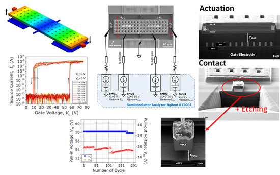
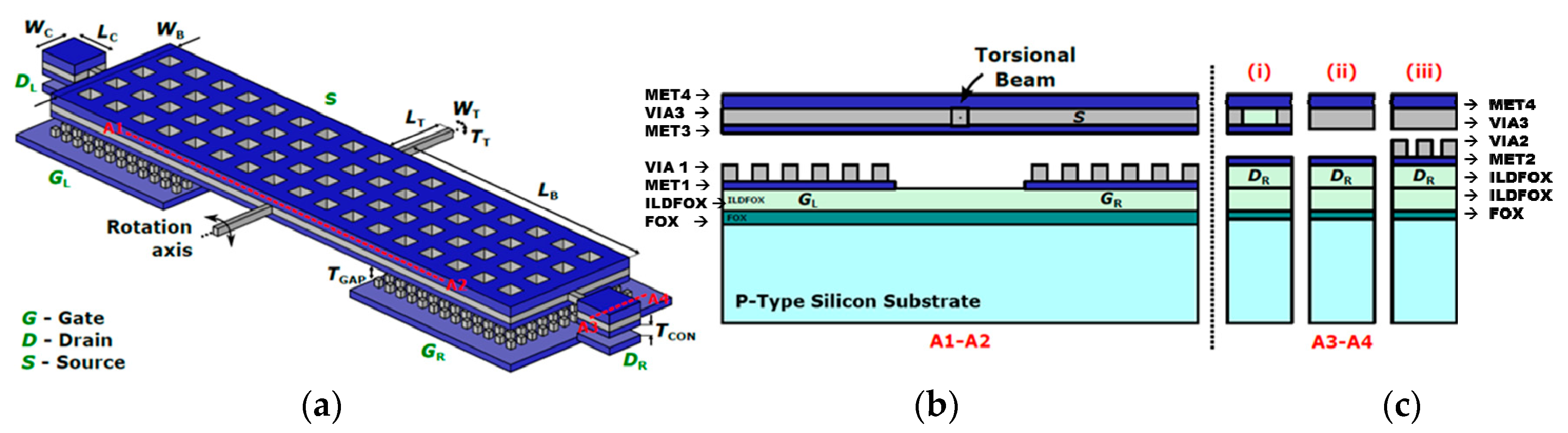
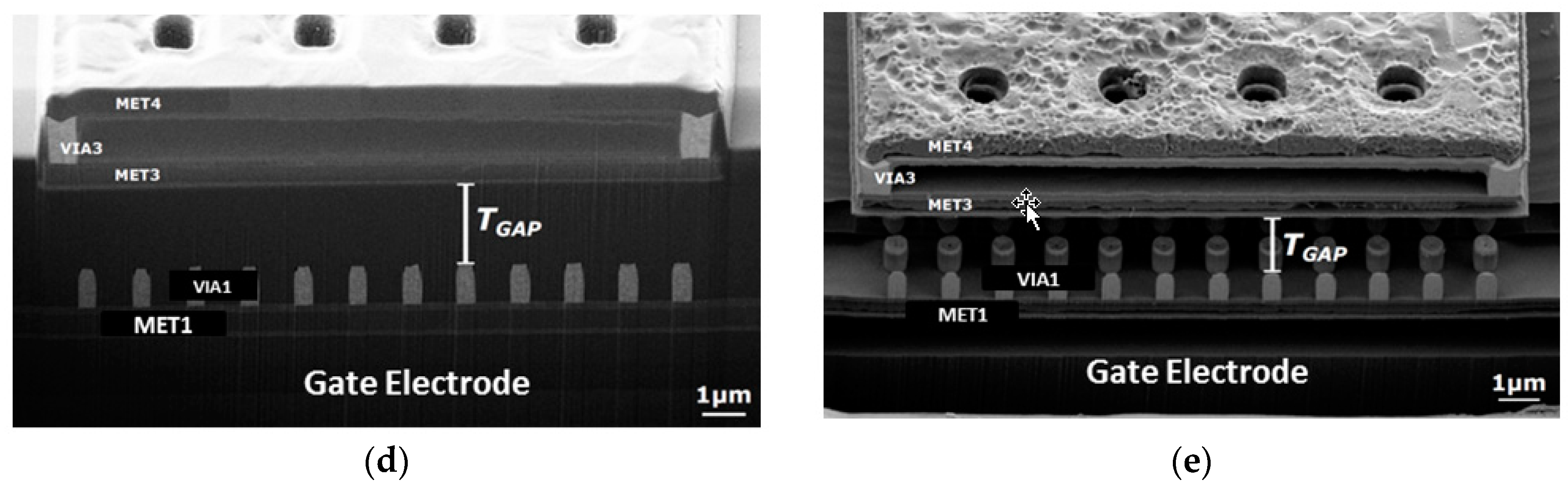
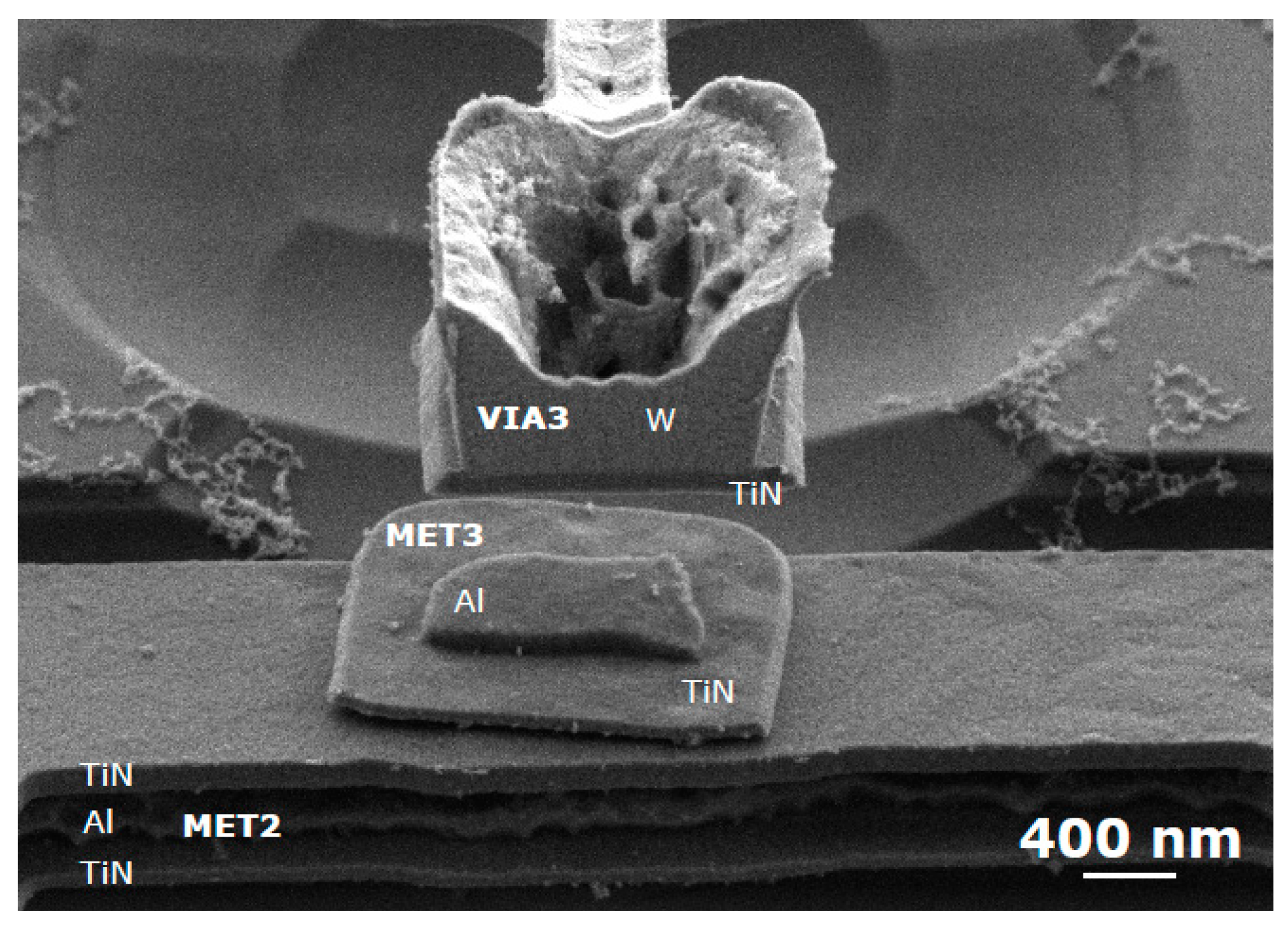
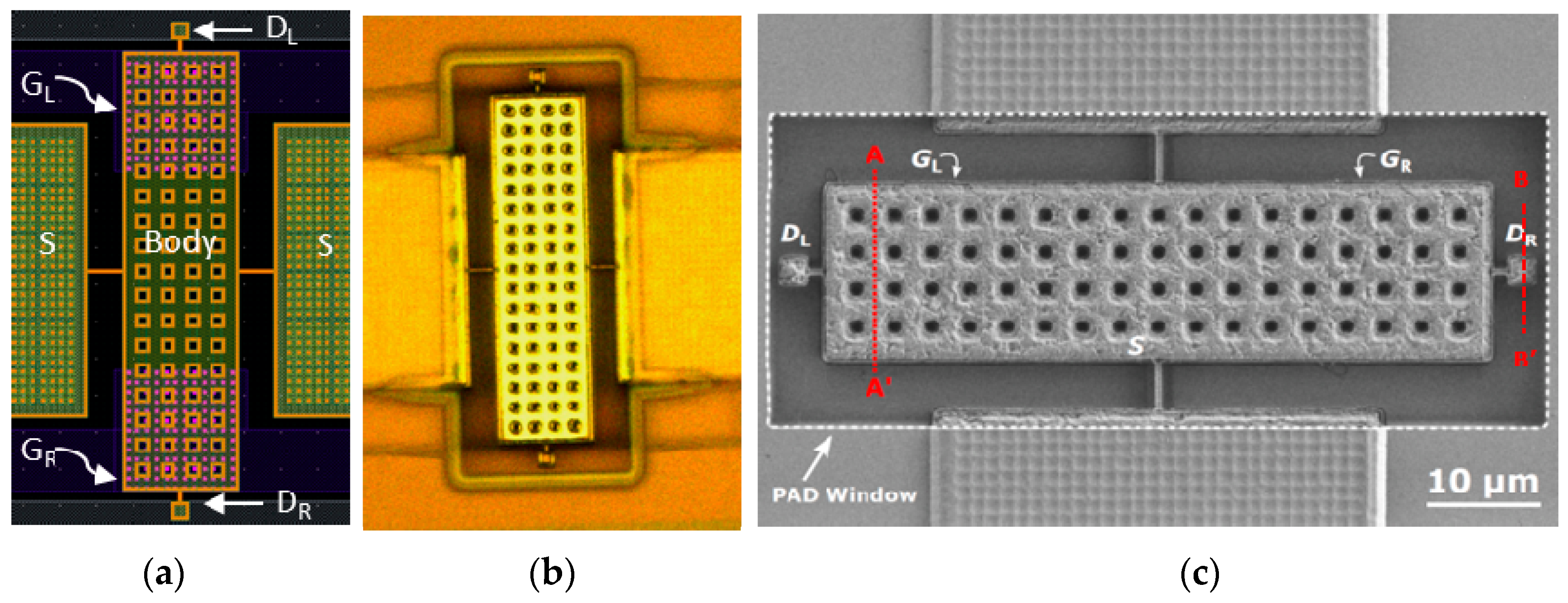
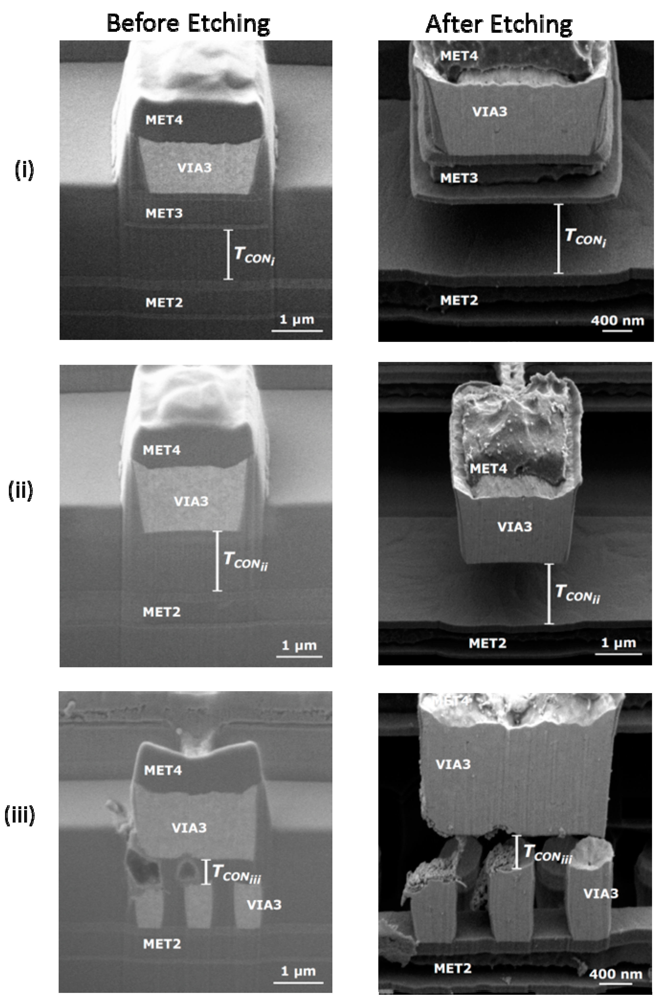
2.1. Device Design and Fabrication
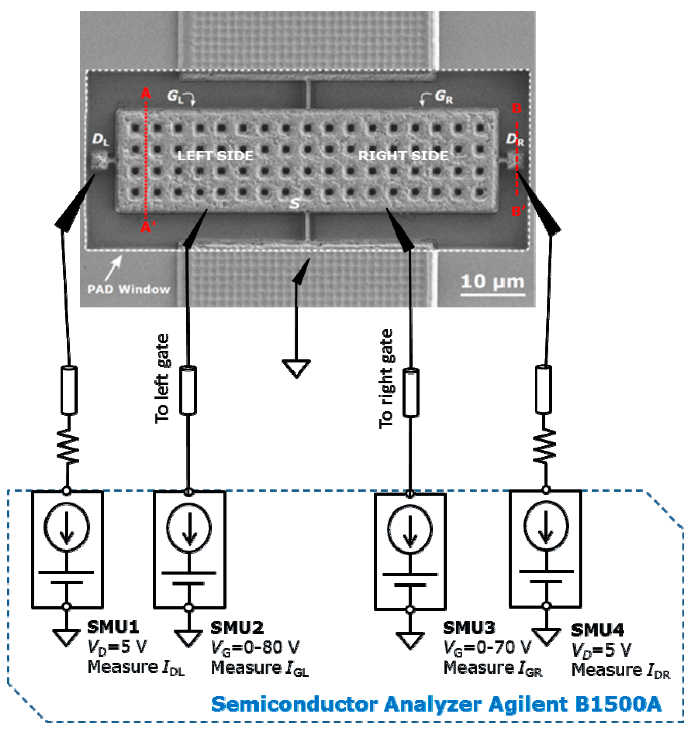
2.2. Electrical Characterization
3. Results
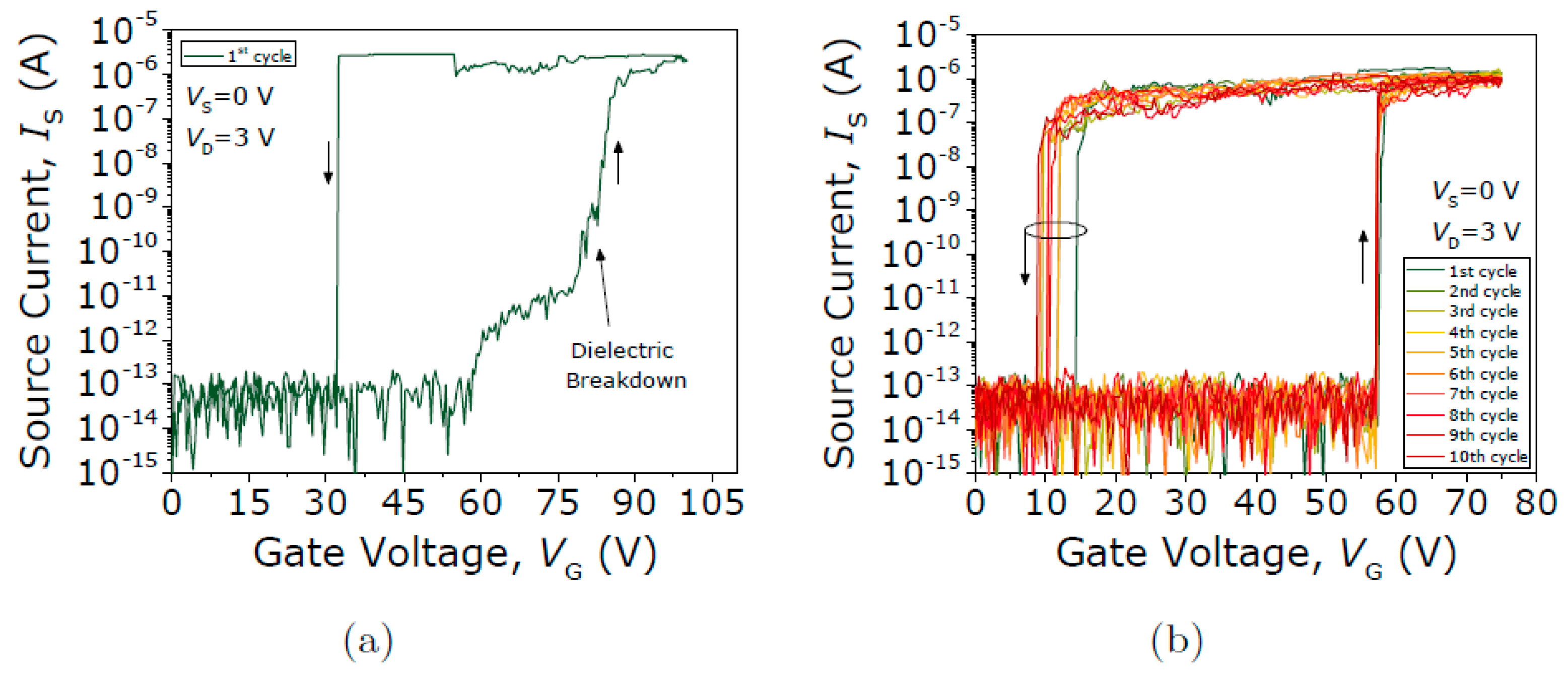
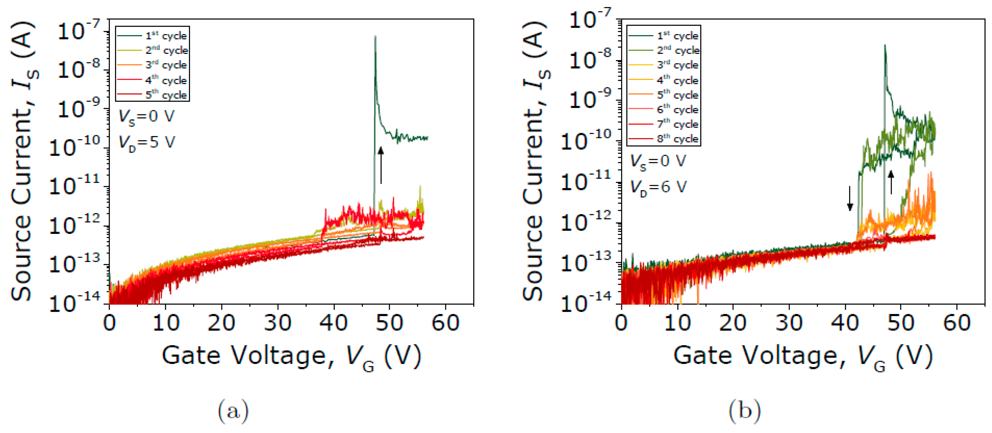
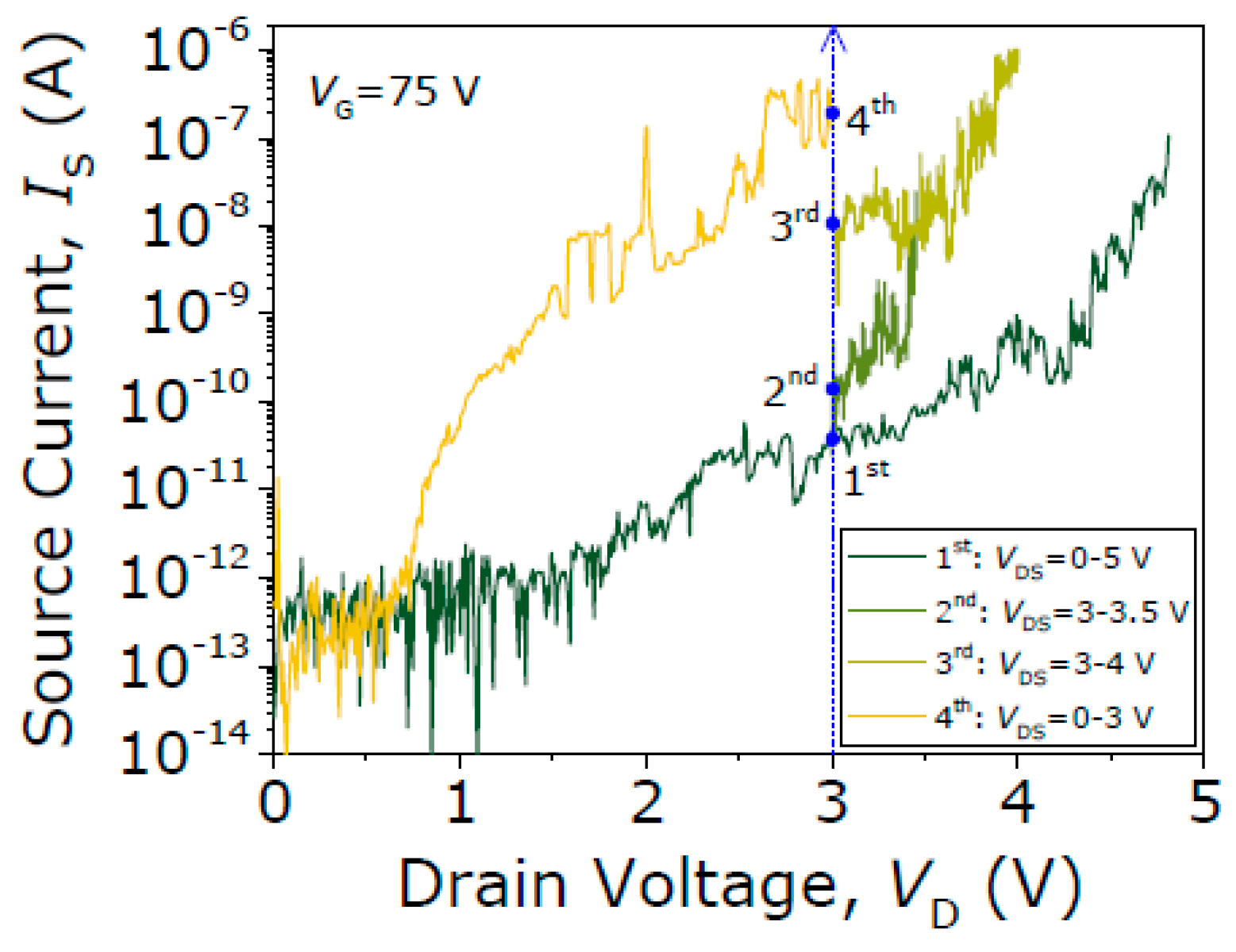
3.1. Seesaw Relay with Contact Type I: TiN vs. TiN
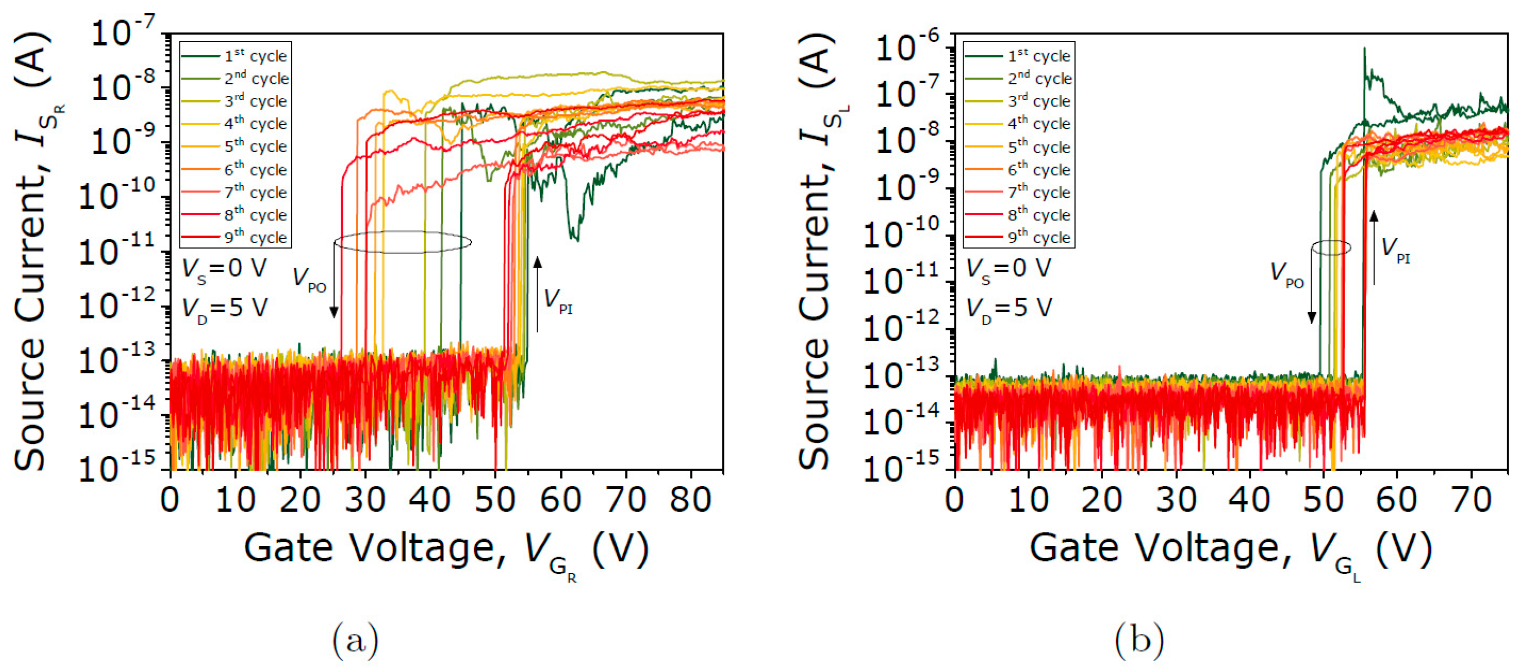
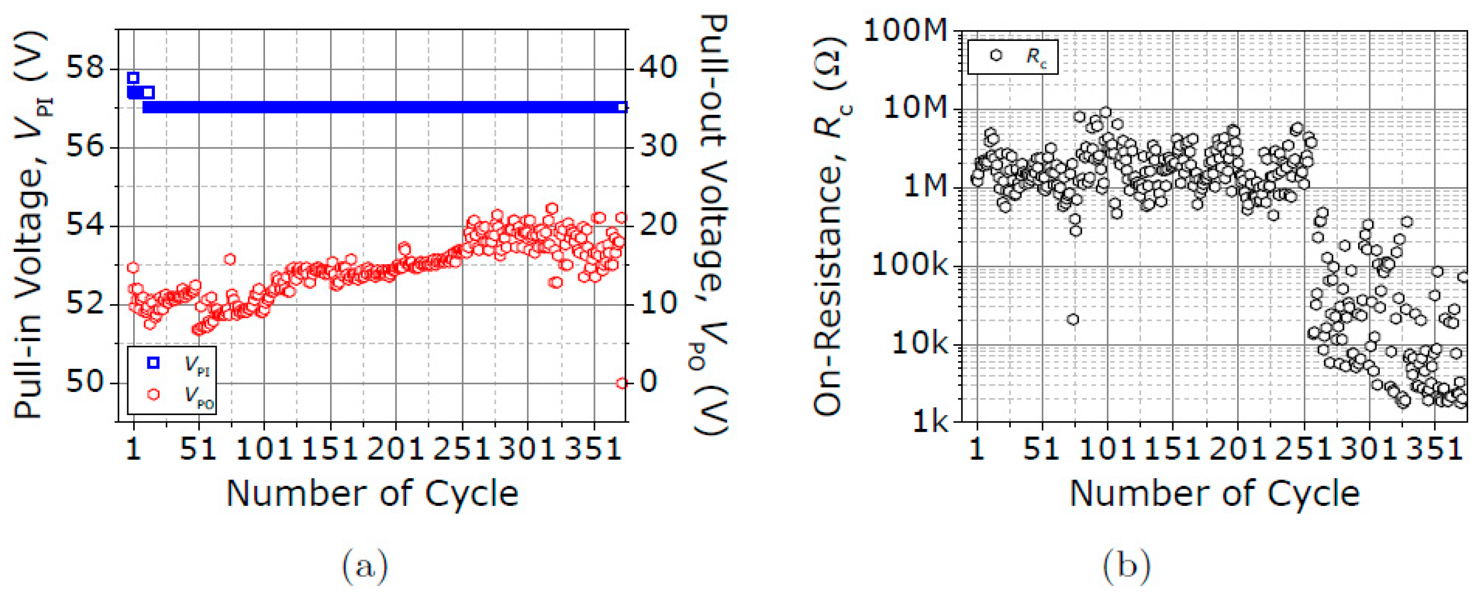
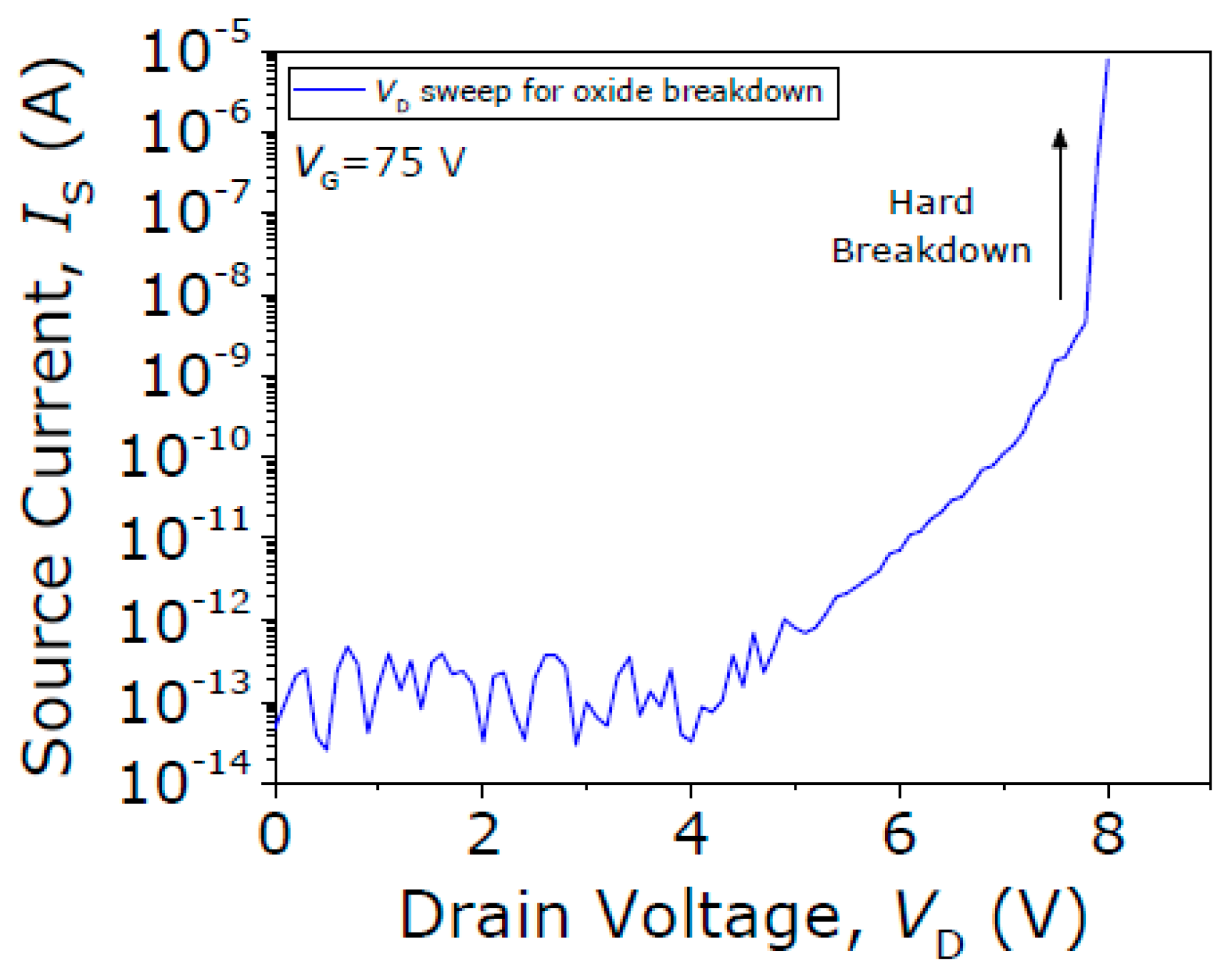
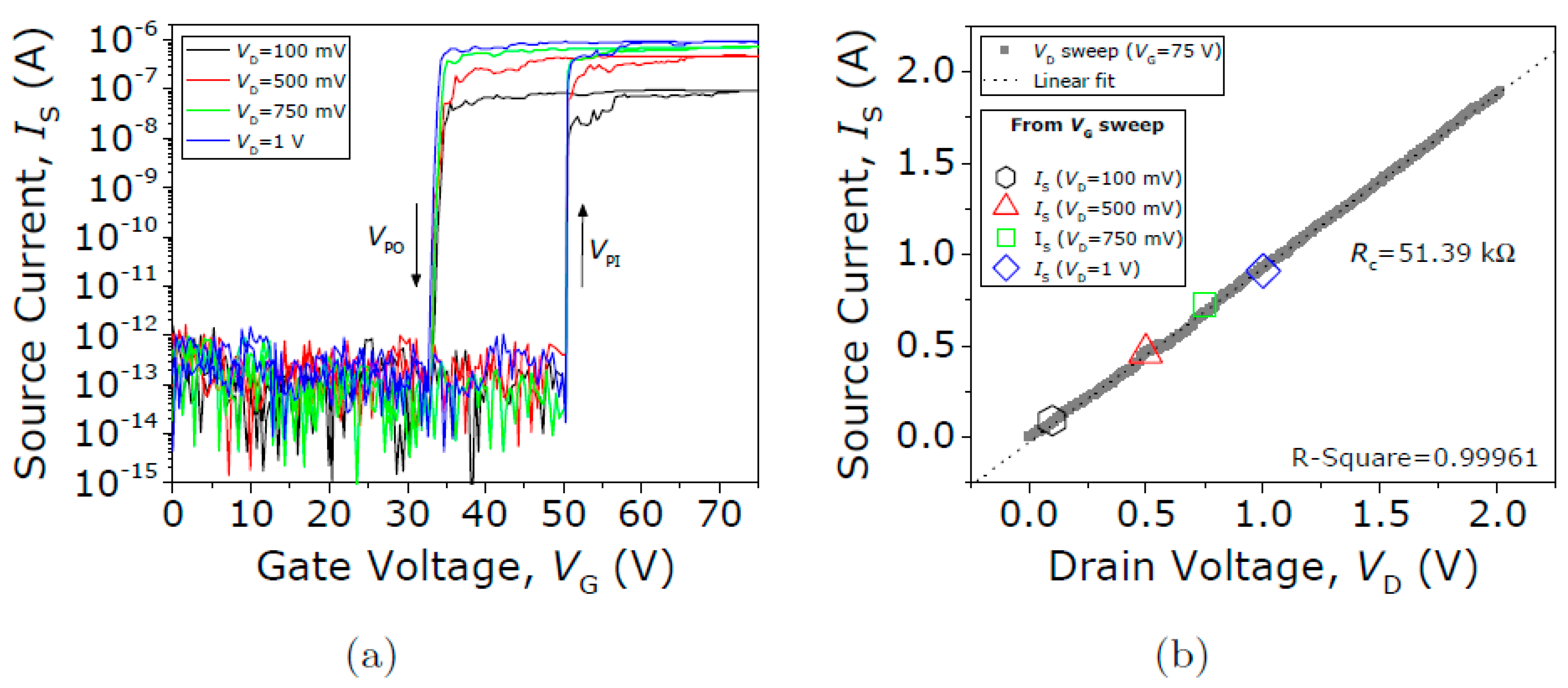
3.2. Seesaw Relay with Contact Type II: W vs. TiN
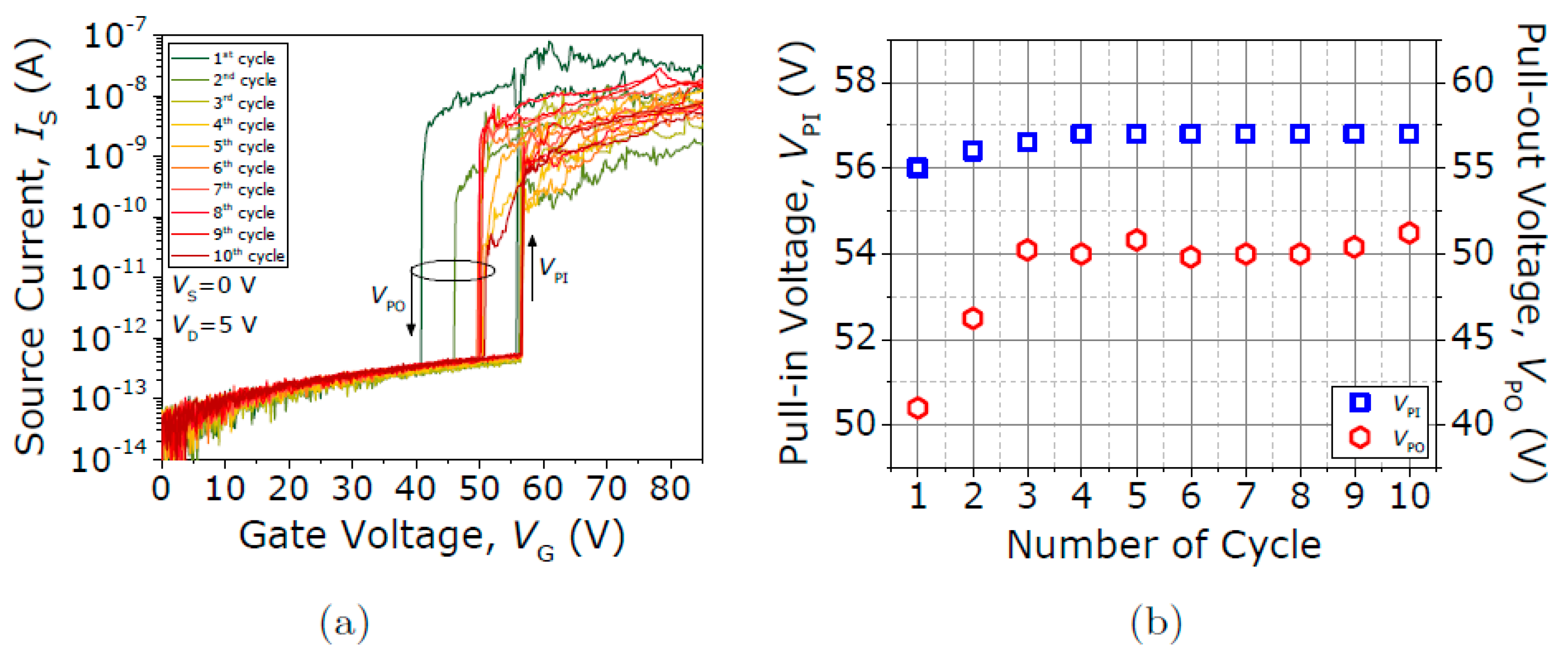
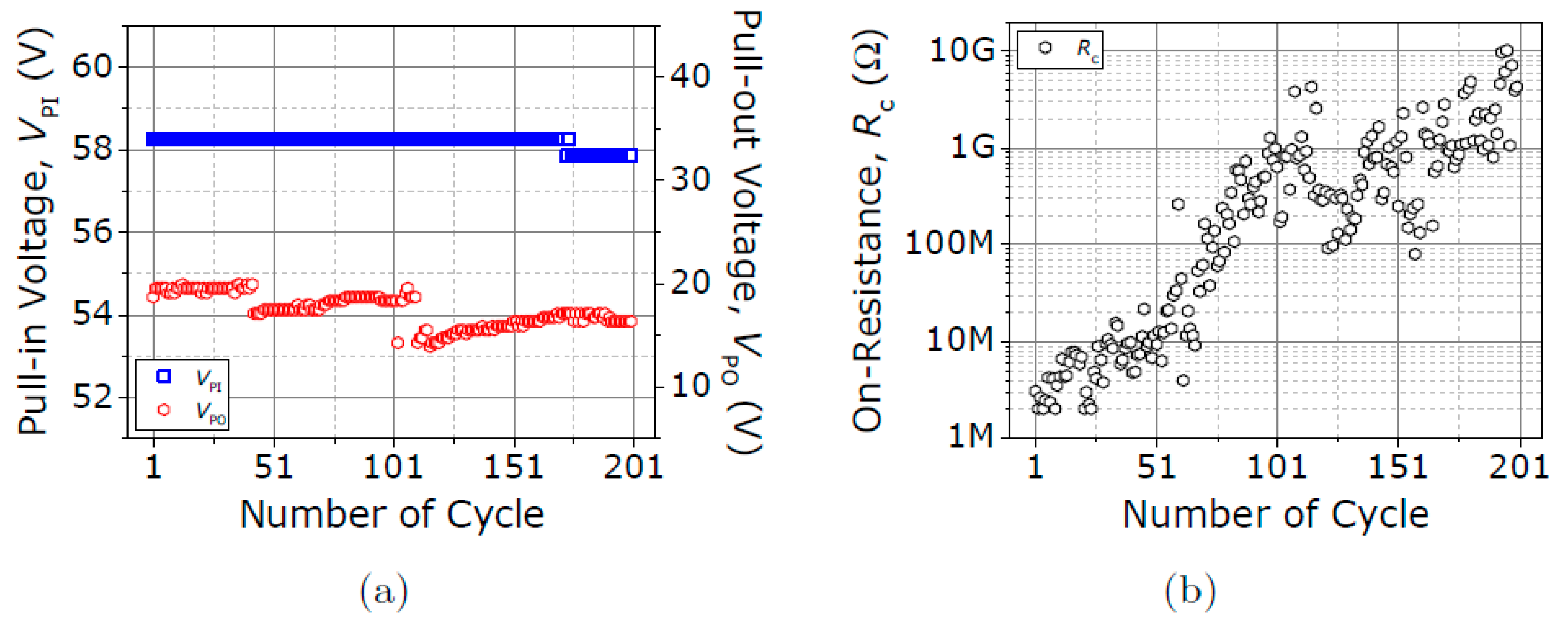
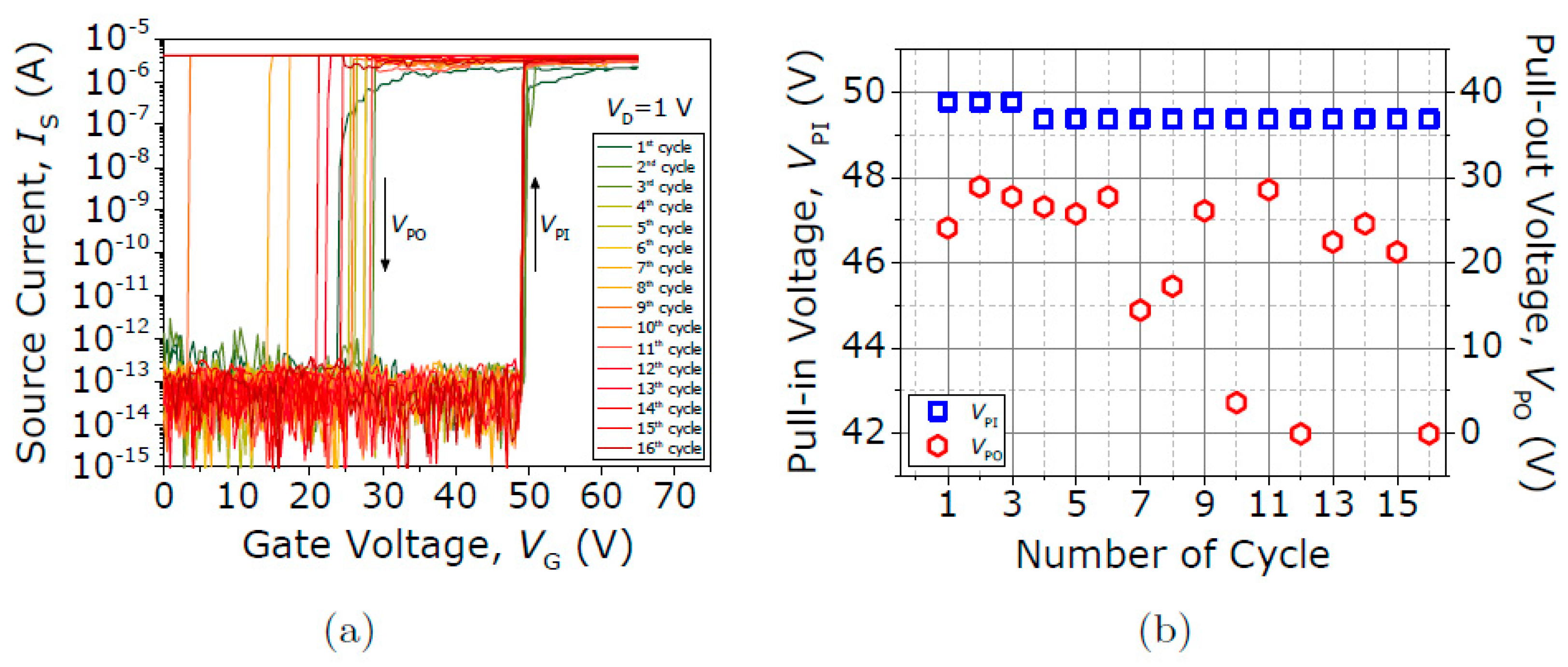
3.3. Seesaw Relay with Contact Type III: W vs. W
4. Discussion and Conclusions
Author Contributions
Funding
Conflicts of Interest
References
- Pott, V.; Kam, H.; Nathanael, R.; Jeon, J.; Alon, E.; King Liu, T.-J. Mechanical computing redux: Relays for integrated circuit applications. Proc. IEEE 2010, 98, 2076–2094. [Google Scholar] [CrossRef]
- King Liu, T.-J.; Xu, N.; Chen, I.-R.; Qian, C.; Fujiki, J. NEM relay design for compact, ultra-low-power digital logic circuits. Proc. IEDM 2014, 13, 1–4. [Google Scholar]
- Spencer, M.; Chen, F.; Wang, C.C.; Nathanael, R.; Fariborzi, H.; Gupta, A.; Kam, H.; Pott, V.; Jeon, J.; King Liu, T.-J.; et al. Demonstration of integrated microelectro-mechanical relay circuits for VLSI applications. IEEE J. Solid-State Circuits 2011, 46, 308–320. [Google Scholar] [CrossRef]
- Qian, C.; Peschot, A.; Osoba, B.; Ye, Z.A.; King Liu, T.-J. Sub-100 mV computing with electro-mechanical relays. IEEE Trans. Electron Devices 2017, 64, 1323–1329. [Google Scholar] [CrossRef]
- Lee, D.; Lee, W.S.; Chen, C.; Fallah, F.; Provine, J.; Chong, S.; Watkins, J.; Wong, H.-S.P.; Howe, R.T.; Mitra, S. Combinatorial logic design using six-terminal NEM relays. IEEE Trans. Comput.-Aided Des. 2013, 32, 655–666. [Google Scholar]
- King Liu, T.-J.; Sikder, U.; Kato, K.; Stojanovic, V. There is plenty of room at the top. In Proceedings of the IEEE International Conference on Micro Electro Mechanical Systems, Las Vegas, NA, USA, 22–26 January 2017; pp. 2–5. [Google Scholar]
- Xu, N.; Sun, J.; Chen, I.-R.; Hutin, L.; Chen, Y.; Fujiki, J.; Qian, C.; King Liu, T.-J. Hybrid CMOS/BEOL-NEMS technology for ultra-low-power IC applications. Proc. IEDM 2014, 28, 1–4. [Google Scholar]
- Ramezani, M.; Severi, S.; Moussa, A.; Osman, H.; Harrie Tilmans, A.C.; De Meyer, K. Contact reliability improvement of a poly-SiGe based nano-relay with titanium nitride coating. In Proceedings of the 18th International Conference on Solid-State Sensors, Actuators and Microsystems (TRANSDUCERS), Anchorage, AK, USA, 21–25 June 2015; pp. 576–579. [Google Scholar]
- Shavezipur, M.; Lee, W.S.; Harrinson, K.L.; Provine, J.; Mitra, S.; Wong, H.-S.P.; Howe, R.T. Laterally actuated nanoelectromechanical relays with compliant, low resistance contact. In Proceedings of the IEEE 26th International Conference on Micro Electro Mechanical Systems (MEMS), Taipei, Taiwan, 20–24 January 2013; pp. 520–523. [Google Scholar]
- Lee, J.O.; Song, Y.H.; Kim, M.W.; Kang, M.H.; Oh, J.S.; Yang, H.H.; Yoon, J.B. A sub-1-volt nanoelectromechanical switching device. Nat. Nanotechnol. 2013, 8, 36. [Google Scholar] [CrossRef] [PubMed]
- Chong, S.; Lee, B.; Parizi, K.B.; Provine, J.; Mitra, S.; Howe, R.T.; Wong, H.S.P. Integration of Nanoelectromechanical (NEM) Relays with Silicon CMOS with Functional CMOS-NEM Circuit. In Proceedings of the International Electron Devices Meeting, Washington, DC, USA, 5–7 December 2011. [Google Scholar]
- Jang, W.W.; Lee, J.O.; Yoon, J.B.; Kim, M.S.; Lee, J.M.; Kim, S.M.; Cho, K.H.; Kim, D.W.; Park, D.; Lee, W.S. Fabrication and Characterization of a nanoelectromechanical switch with 15 nm thick suspension air gap. Appl. Phys. Lett. 2008, 92, 103110. [Google Scholar] [CrossRef]
- Riverola, M.; Sobreviela, G.; Torres, F.; Uranga, A.; Barniol, N. A monolithically integrated torsional CMOS-MEMS relay. J. Micromech. Microeng. 2016, 26, 115012. [Google Scholar] [CrossRef]
- Riverola, M.; Uranga, A.; Torres, F.; Barniol, N. Fabrication and characterization of a hammer-shaped CMOS/BEOL-embedded nanoelectromechanical (NEM) relay. Microelectron. Eng. 2018, 92, 44–51. [Google Scholar] [CrossRef]
- Riverola, M.; Vidal-Álvarez, G.; Sobreviela, G.; Uranga, A.; Torres, F.; Barniol, N. Dynamic Properties of Three-Terminal Tungsten CMOS-NEM Relays Under Nonlinear Tapping Mode. IEEE Sens. J. 2016, 16, 5283–5291. [Google Scholar] [CrossRef]
- Lee, J.-O.; Kim, M.-W.; Ko, S.-D.; Yoon, J.-B. Annealing effect on contact characteristics in TiN based 3-terminal NEM relays. In Proceedings of the 10th IEEE International Conference on Nanotechnology, Seoul, South Korea, 17–20 August 2010; pp. 258–261. [Google Scholar]
- Muñoz-Gamarra, J.L.; Uranga, A.; Barniol, N. Nanomechanical switches based on metal-insulator-metal capacitors from standard complementary-metal-oxide semiconductor technology. Appl. Phys. Lett. 2014, 104, 243105. [Google Scholar] [CrossRef]
- Riverola, M.; Sobreviela, G.; Torres, F.; Uranga, A.; Barniol, N. Single-resonator dual frequency BEOL-embedded CMOS-MEMS oscillator with low-power and ultracompact TIA core. IEEE Electron Device Lett. 2017, 38, 273–276. [Google Scholar] [CrossRef]
- Prache, P.; Juillard, J.; Maris Ferreira, P.; Barniol, N.; Riverola, M. Design and characterization of a monolithic CMOS-MEMS mutually injection-locked oscillator for differential resonant sensing. Sens. Actuators A Phys. 2018, 269, 160–170. [Google Scholar] [CrossRef]
- Cai, Z.; van Veldhoven, R.; Suy, H.; de Graaf, G.; Makinwa, K.A.A.; Pertijs, M.A.P. A Phase-Domain Readout Circuit for a CMOS-Compatible Hot-Wire CO2 Sensor. IEEE J. Solid State Circuits 2018, 53, 3303–3313. [Google Scholar] [CrossRef]
- Uranga, A.; Verd, J.; Barniol, N. CMOS–MEMS resonators: From devices to applications. Microelectron. Eng. 2015, 132, 58–73. [Google Scholar] [CrossRef]
- Ching-Liang, D. A maskless wet etching silicon dioxide post-CMOS process and its application. Microelectron. Eng. 2006, 83, 2543–2550. [Google Scholar]
- Uranga, A.; Sobreviela, G.; Riverola, M.; Torres, F.; Barniol, N. Phase-Noise Reduction in a CMOS-MEMS Oscillator under Nonlinear MEMS Operation. IEEE Trans. Circuits Syst. I Regul. Pap. 2017, 64, 3047–3055. [Google Scholar] [CrossRef]


| Design Parameter | Value (µm) |
|---|---|
| Torsion beam length LT | 4.7 |
| Torsion beam width WT | 0.5 |
| Torsion beam thickness TT | 1.3 |
| Body length LB | 59.6 |
| Body width WB | 16 |
| Electrode length GR,L | 30 |
| Electrode width GW | 16 |
| Contact length LC | 2.5 |
| Contact width WC | 2.5 |
| Actuation gap TGap | 1.95 |
| Contact gap (i) Tcon | 1 |
| Contact gap (ii) Tcon | 1.3 a |
| Contact gap (iii) Tcon | 0.45 a |
| Torsional Mode | Vertical Mode | |
|---|---|---|
| Mode Shape | 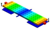 | 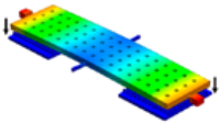 |
| Resonant Frequency, f0 Spring Constant, keff | 152 kHz 1.28 N/m | 1.5 MHz 69.6 N/m |
| Device | SEM Image Structural/Material | Contact Material | VPI (V) | ON-OFF Ratio | RC (Ω) | Cycles (EOL) |
|---|---|---|---|---|---|---|
| This work |  Via3 BEOL-CMOS layers | TiN/TiN | 54.8 a | 105 a | 100 M a | - |
| W/TiN | 57 | 107 | 2 k | 355 | ||
| W/W | 49 | 107 | 51.4 k | 16 | ||
| [13] | 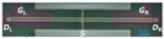 Via3 BEOL-CMOS layers | TiN/TiN | 71.3 | 106 | 20–45 k | 65 |
| [16] | CVD/PVD TiN, CMOS | TiN/TiN (annealed) | 24 | 105 | 500 M | 30 |
| [8] | TiN coated PolySiGe, no CMOS | TiN/SiGe | 15 | 106 | No ohmic contact | 1010 |
| [17] | MIM module, CMOS | TiN/TiN | 5–20 | 104 | 1 G | 10 |
| [9] | TiN coated PolySi, no CMOS | TiN/TiN | 22 | >104 | 4–15 k | 150 |
© 2018 by the authors. Licensee MDPI, Basel, Switzerland. This article is an open access article distributed under the terms and conditions of the Creative Commons Attribution (CC BY) license (http://creativecommons.org/licenses/by/4.0/).
Share and Cite
Riverola, M.; Torres, F.; Uranga, A.; Barniol, N. High Performance Seesaw Torsional CMOS-MEMS Relay Using Tungsten VIA Layer. Micromachines 2018, 9, 579. https://doi.org/10.3390/mi9110579
Riverola M, Torres F, Uranga A, Barniol N. High Performance Seesaw Torsional CMOS-MEMS Relay Using Tungsten VIA Layer. Micromachines. 2018; 9(11):579. https://doi.org/10.3390/mi9110579
Chicago/Turabian StyleRiverola, Martín, Francesc Torres, Arantxa Uranga, and Núria Barniol. 2018. "High Performance Seesaw Torsional CMOS-MEMS Relay Using Tungsten VIA Layer" Micromachines 9, no. 11: 579. https://doi.org/10.3390/mi9110579
APA StyleRiverola, M., Torres, F., Uranga, A., & Barniol, N. (2018). High Performance Seesaw Torsional CMOS-MEMS Relay Using Tungsten VIA Layer. Micromachines, 9(11), 579. https://doi.org/10.3390/mi9110579