

A Review of Tunnel Field-Effect Transistors: Materials, Structures, and Applications


Abstract
1. Introduction
2. Experiment Research Works on TFETs
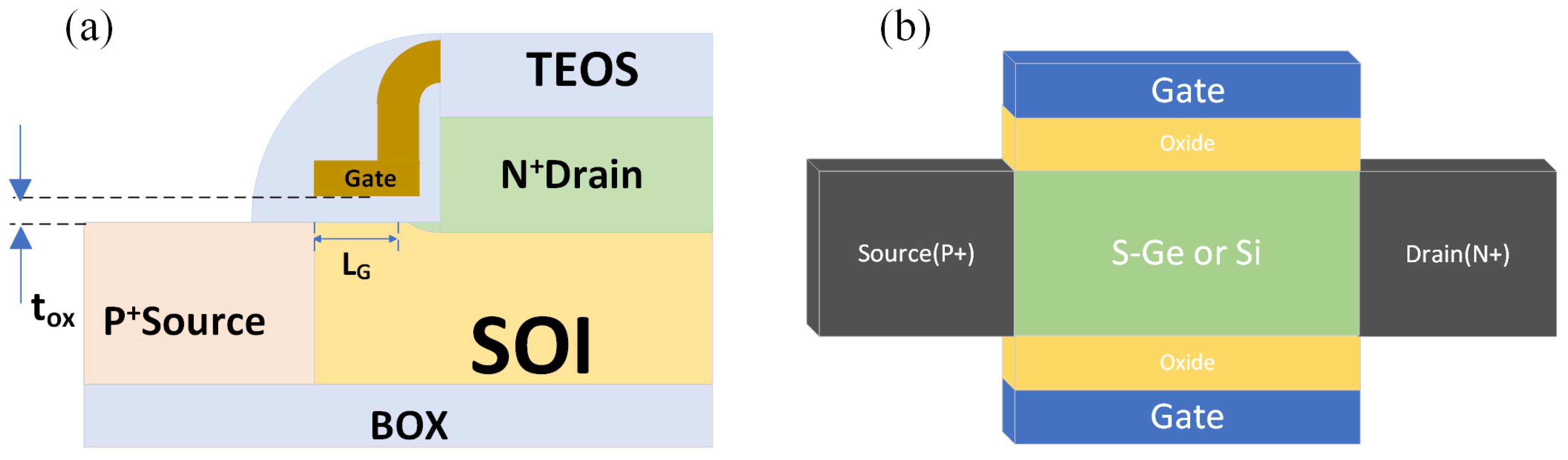
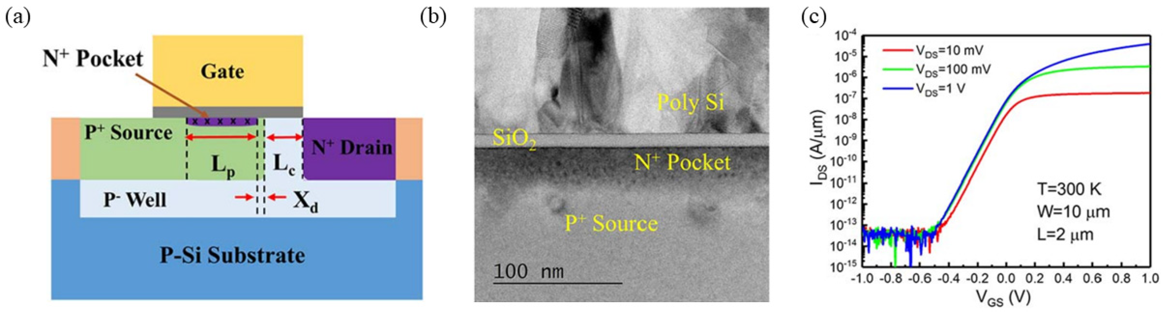
2.1. Si/Ge-Based TFETs
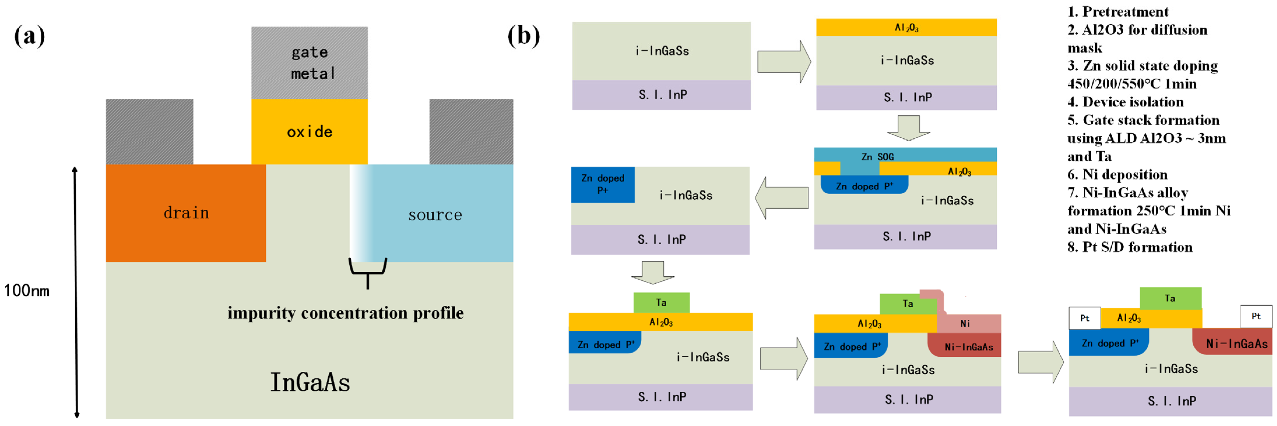
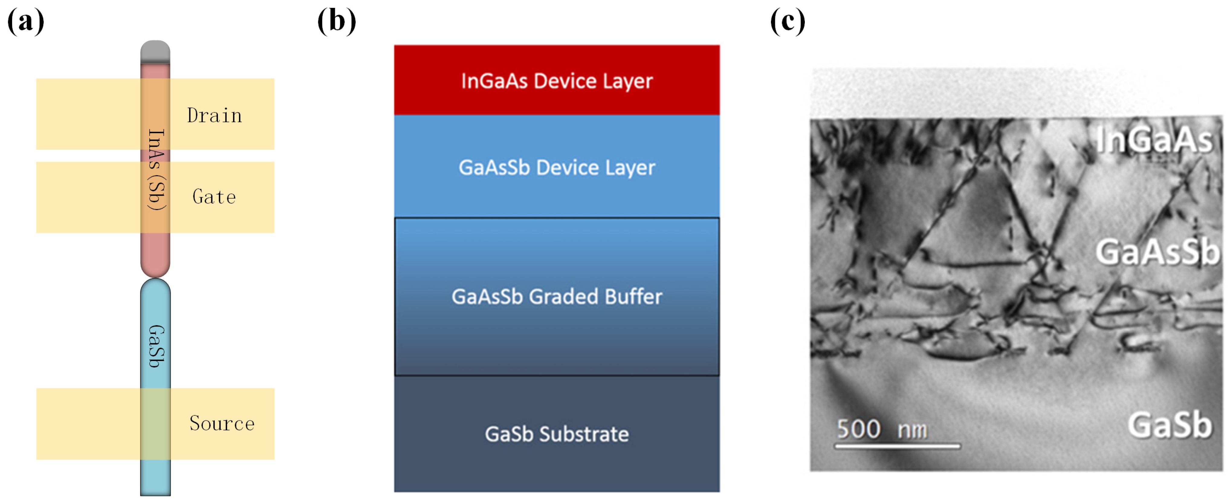
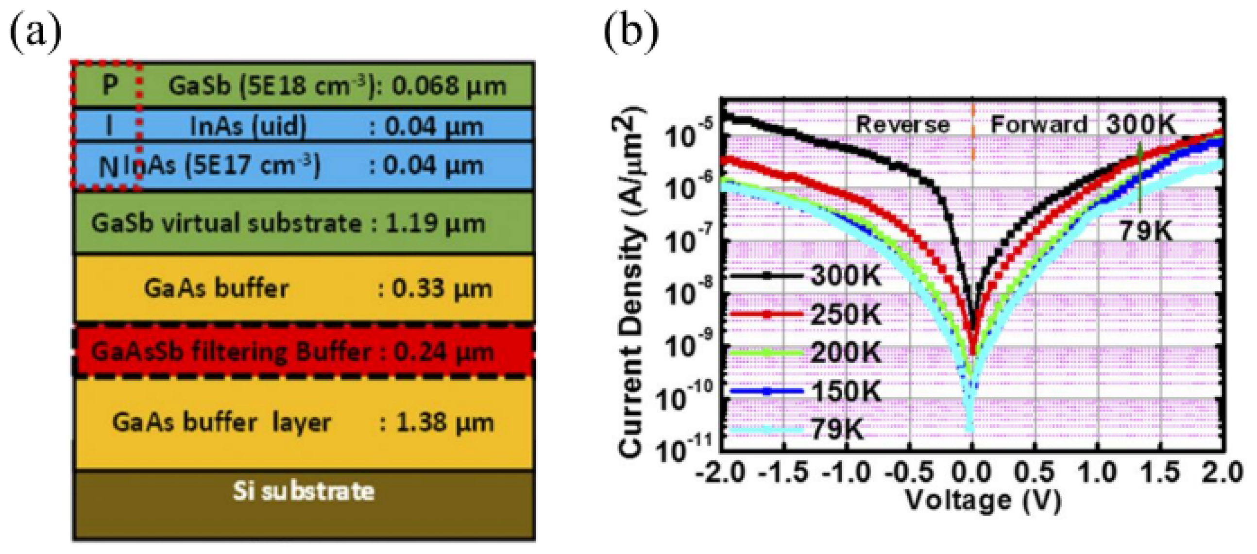
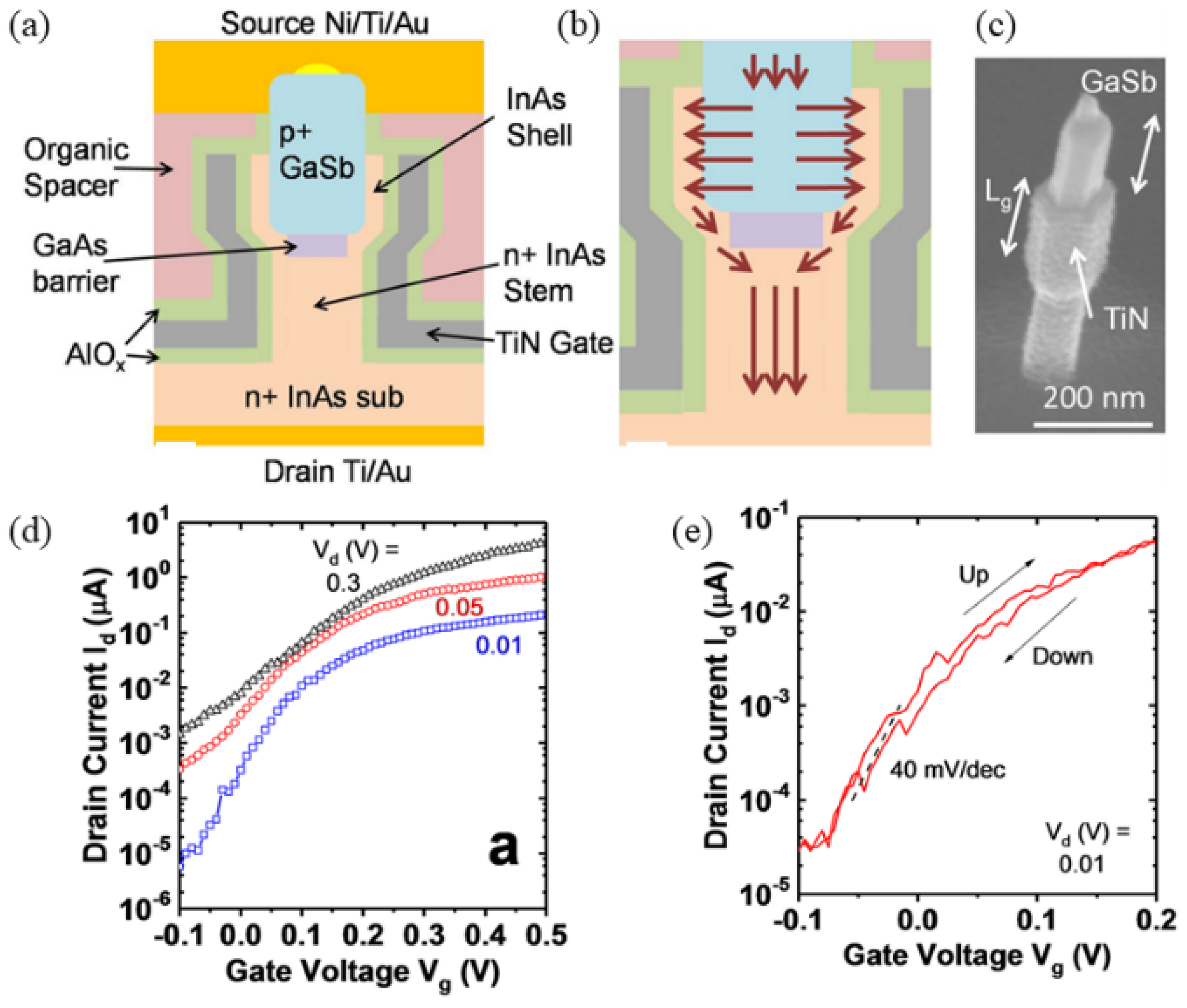
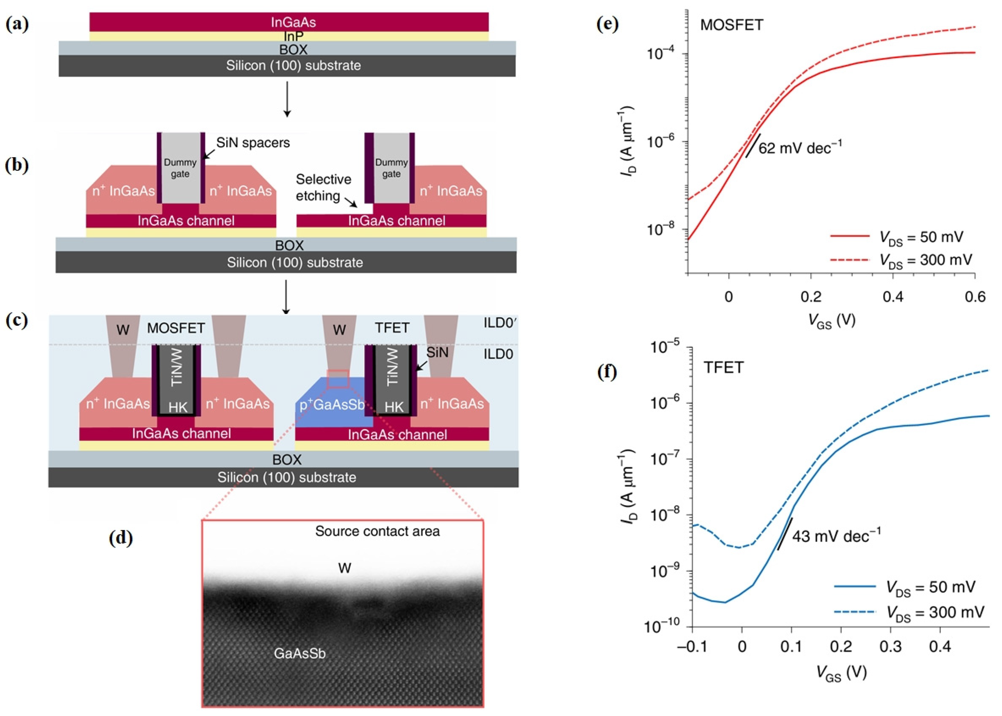
2.2. Heterojunction TFETs Based on III-V Compounds
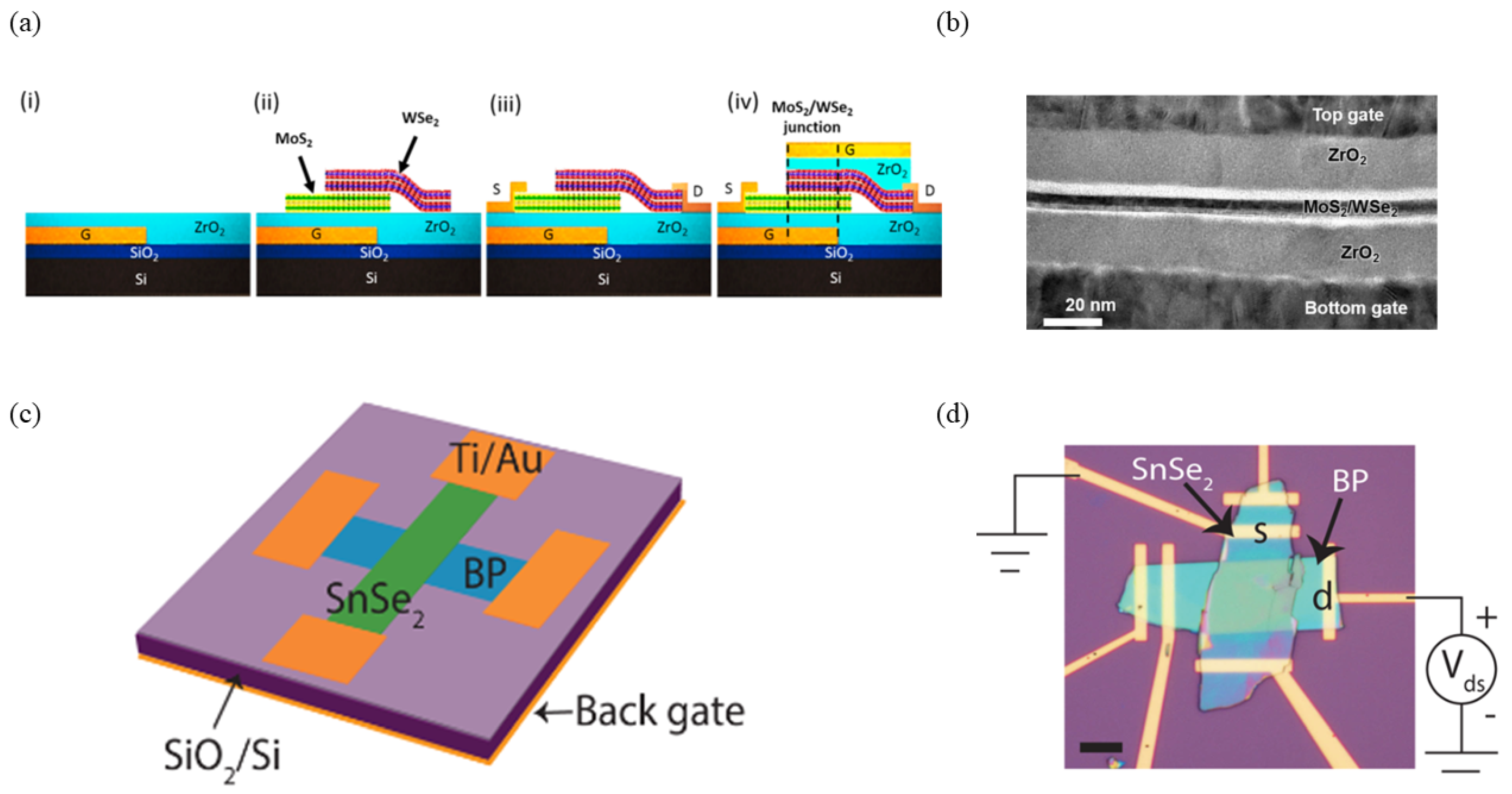
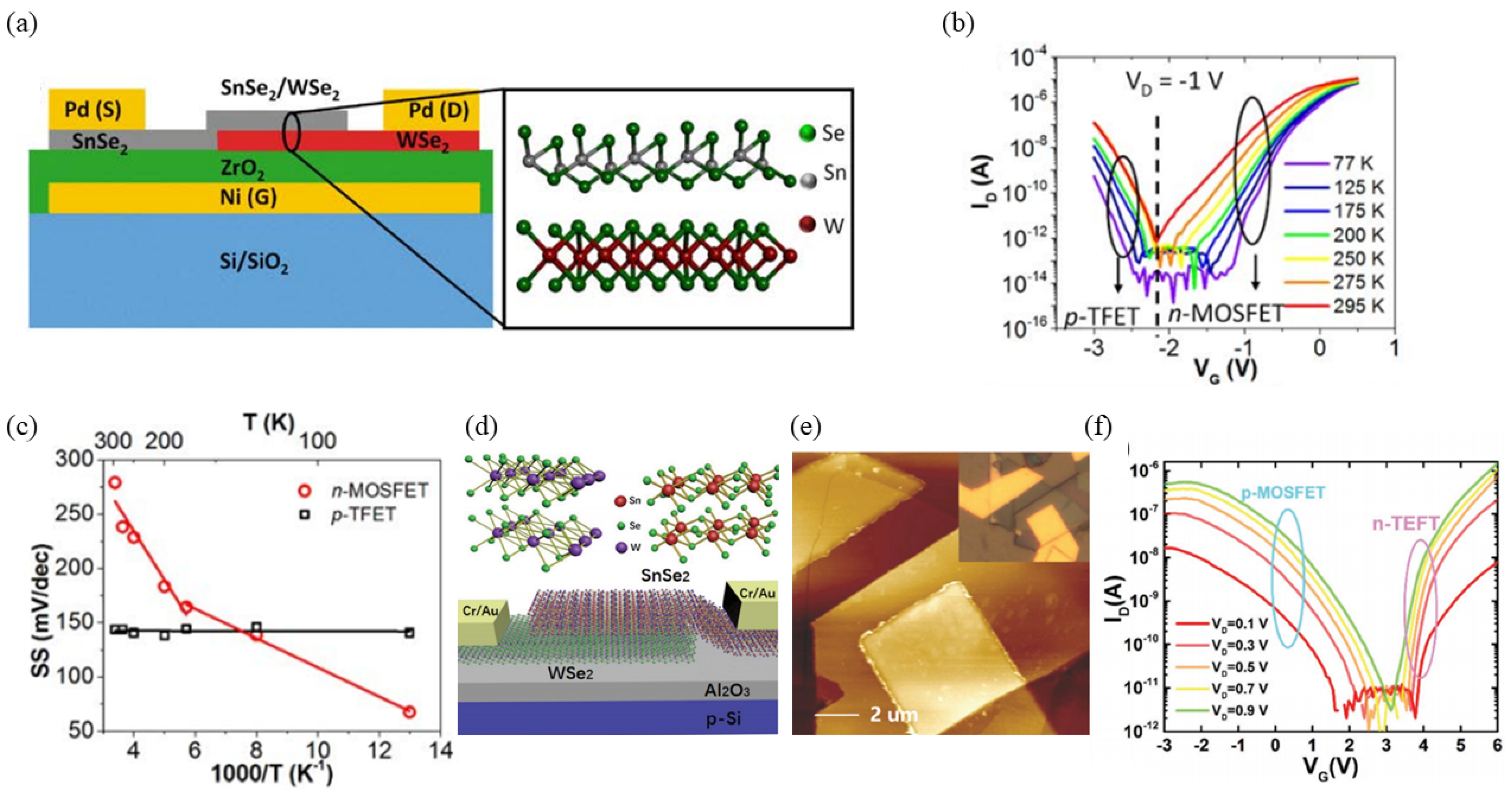
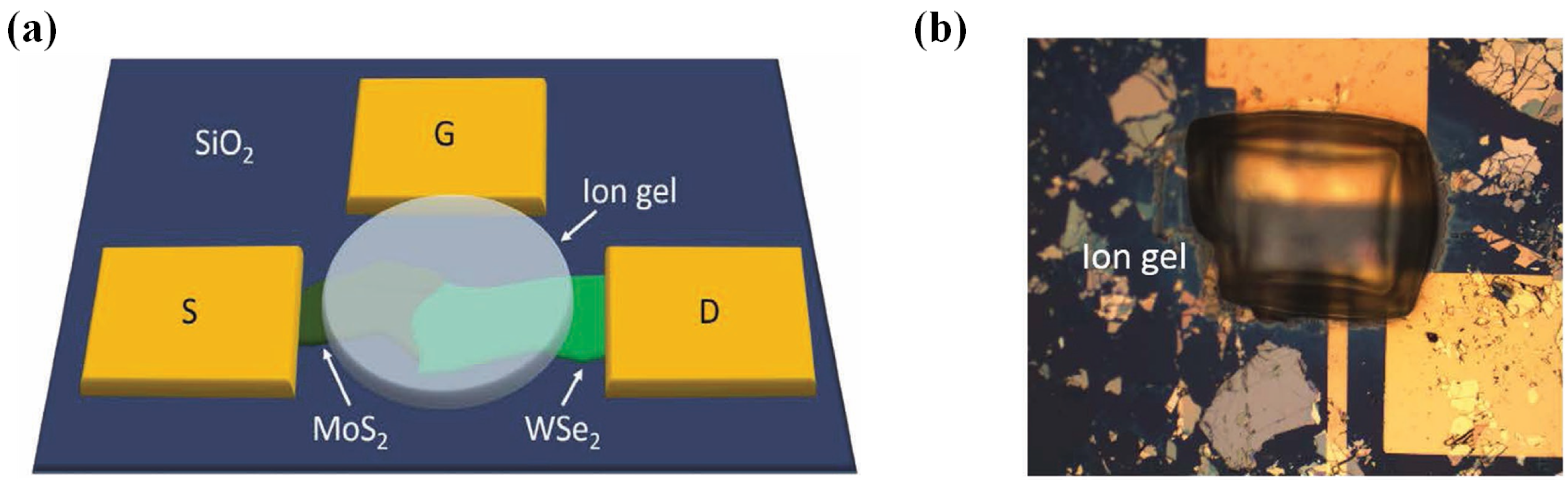
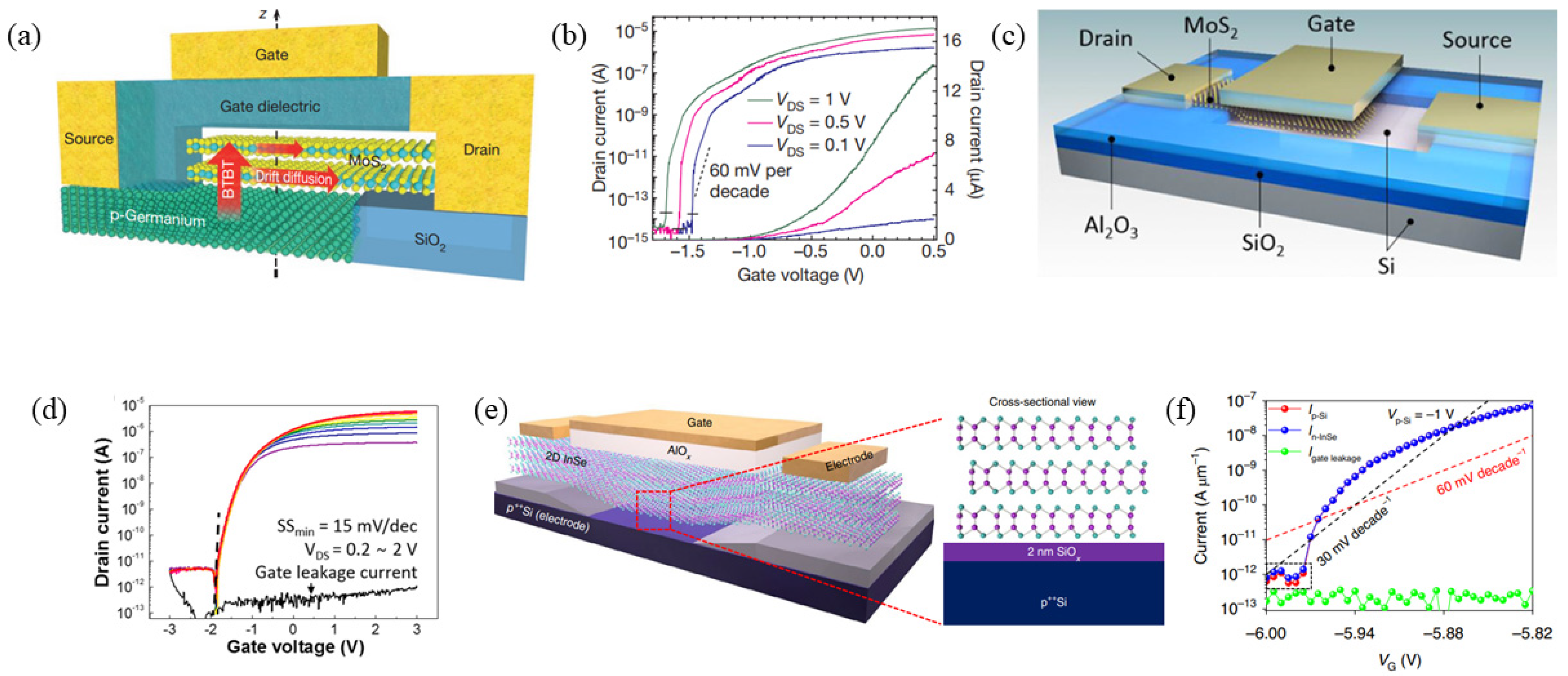
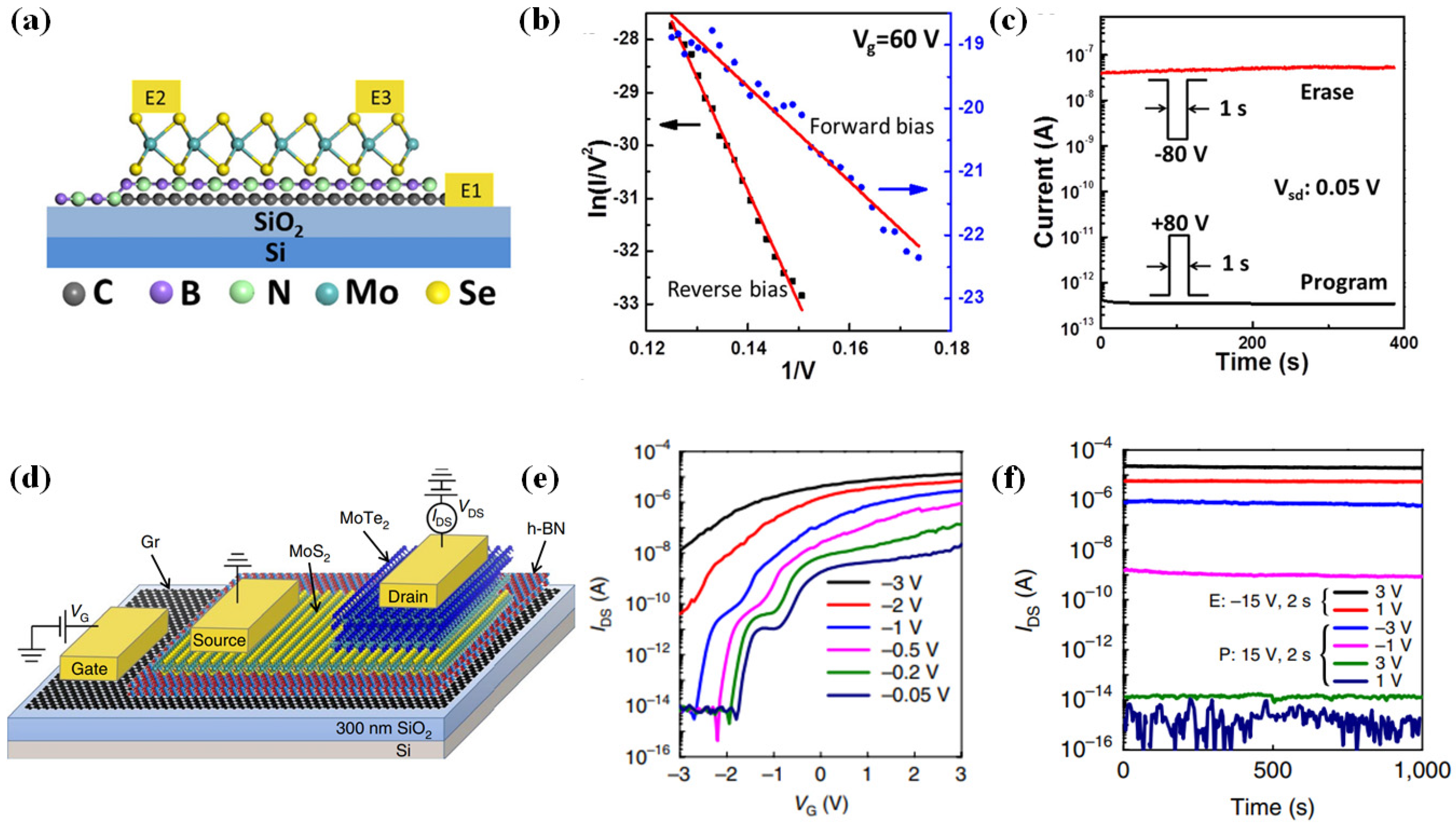
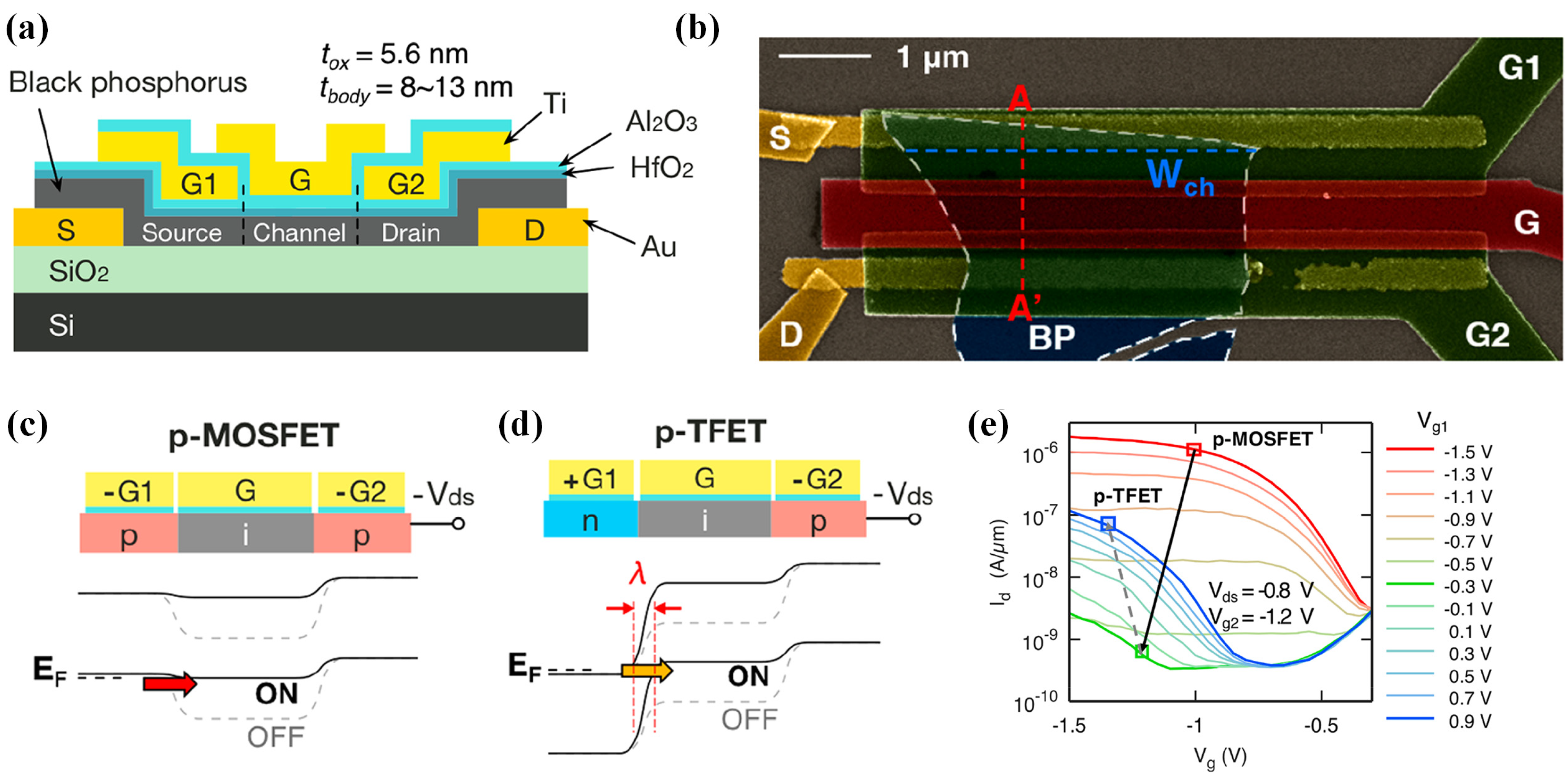
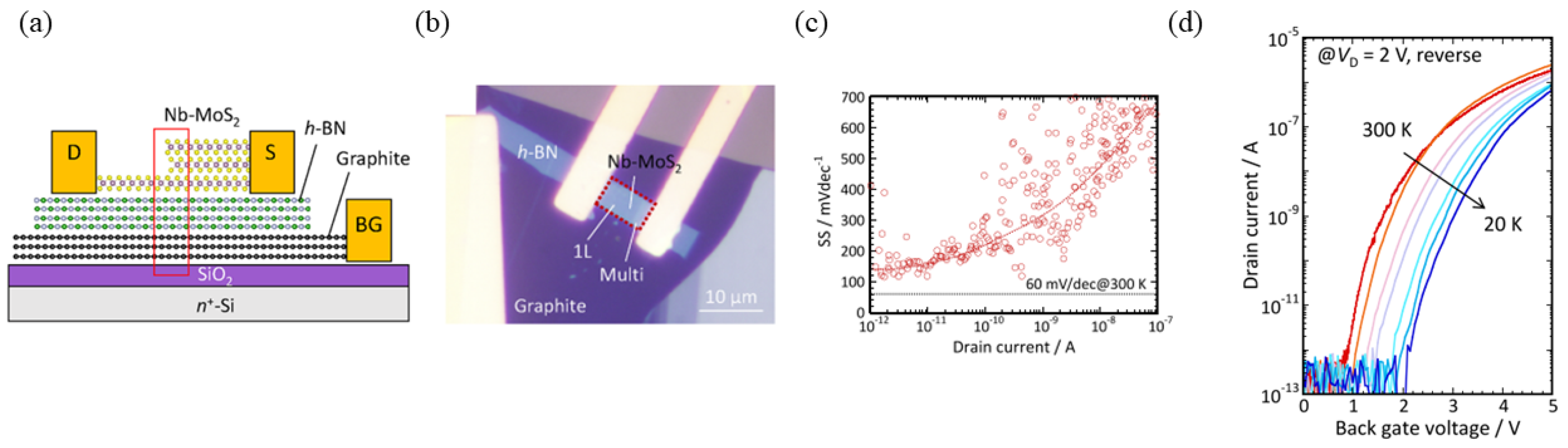
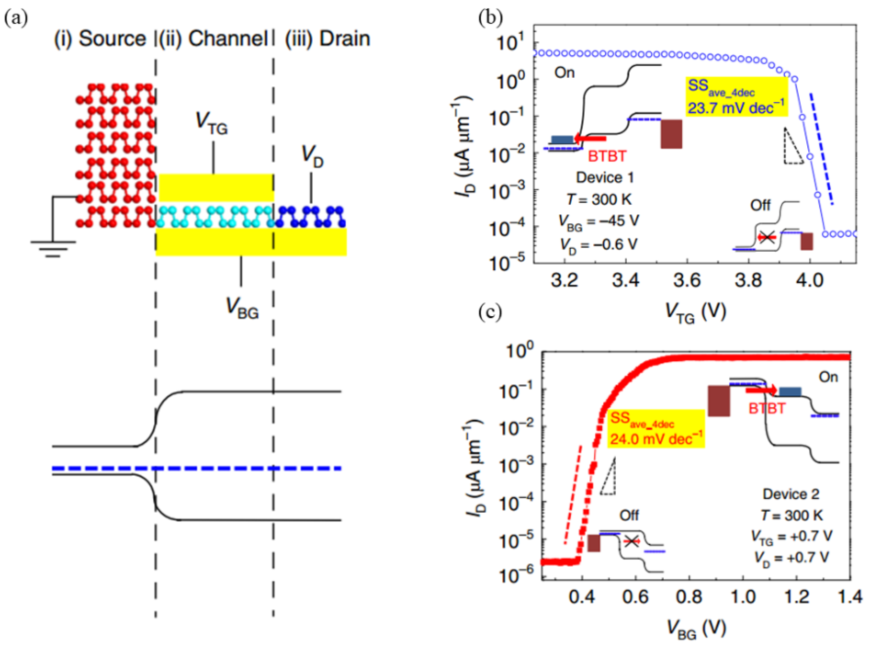
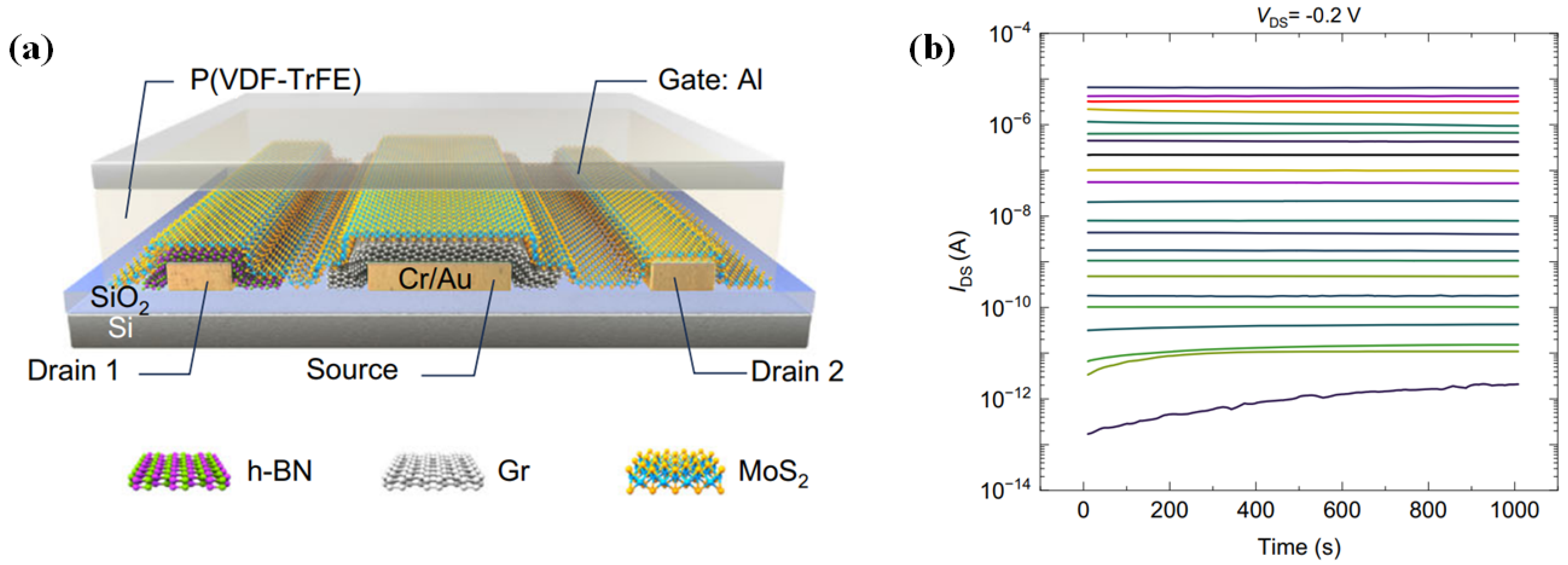
2.3. TFETs Based on 2D Materials
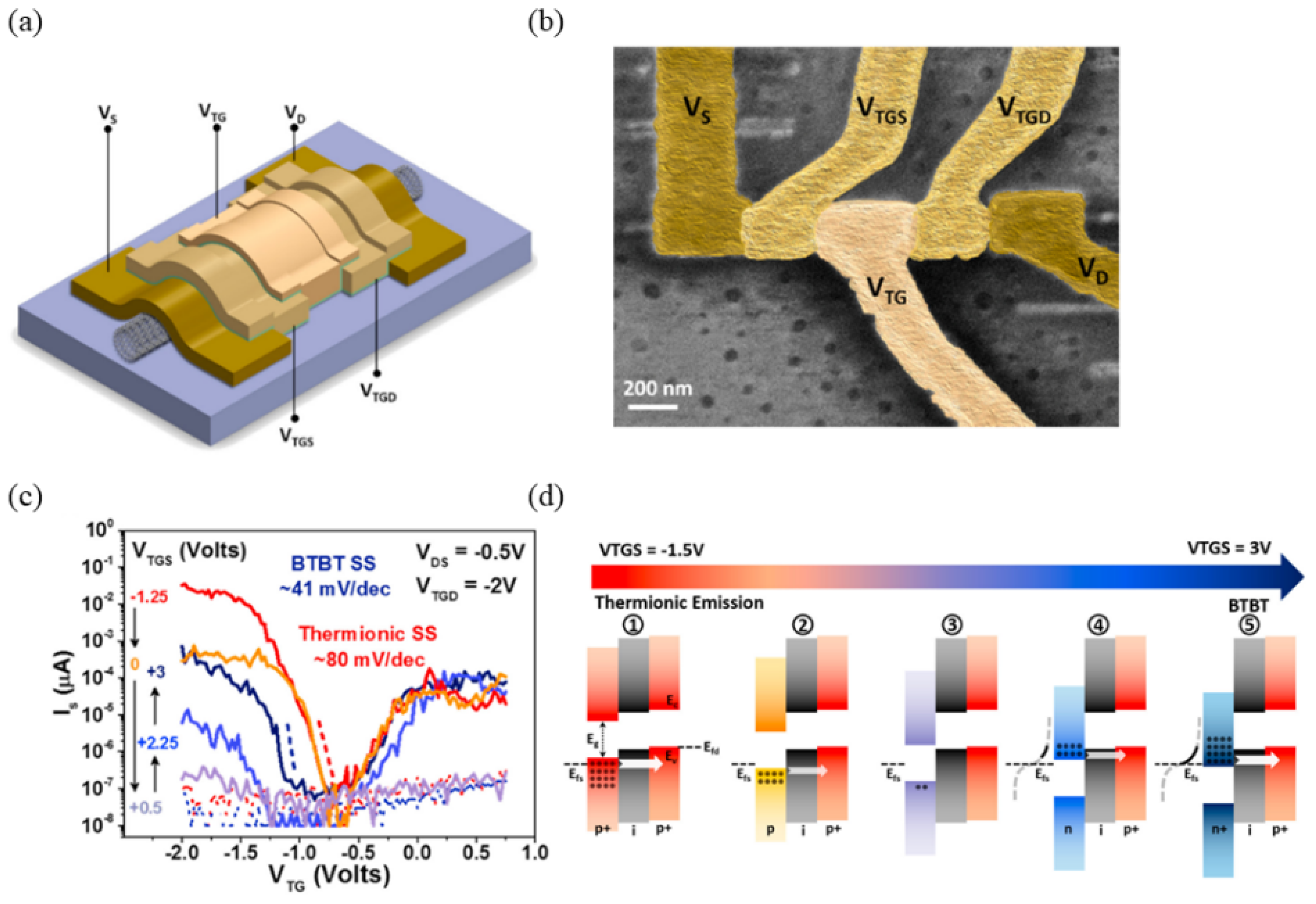
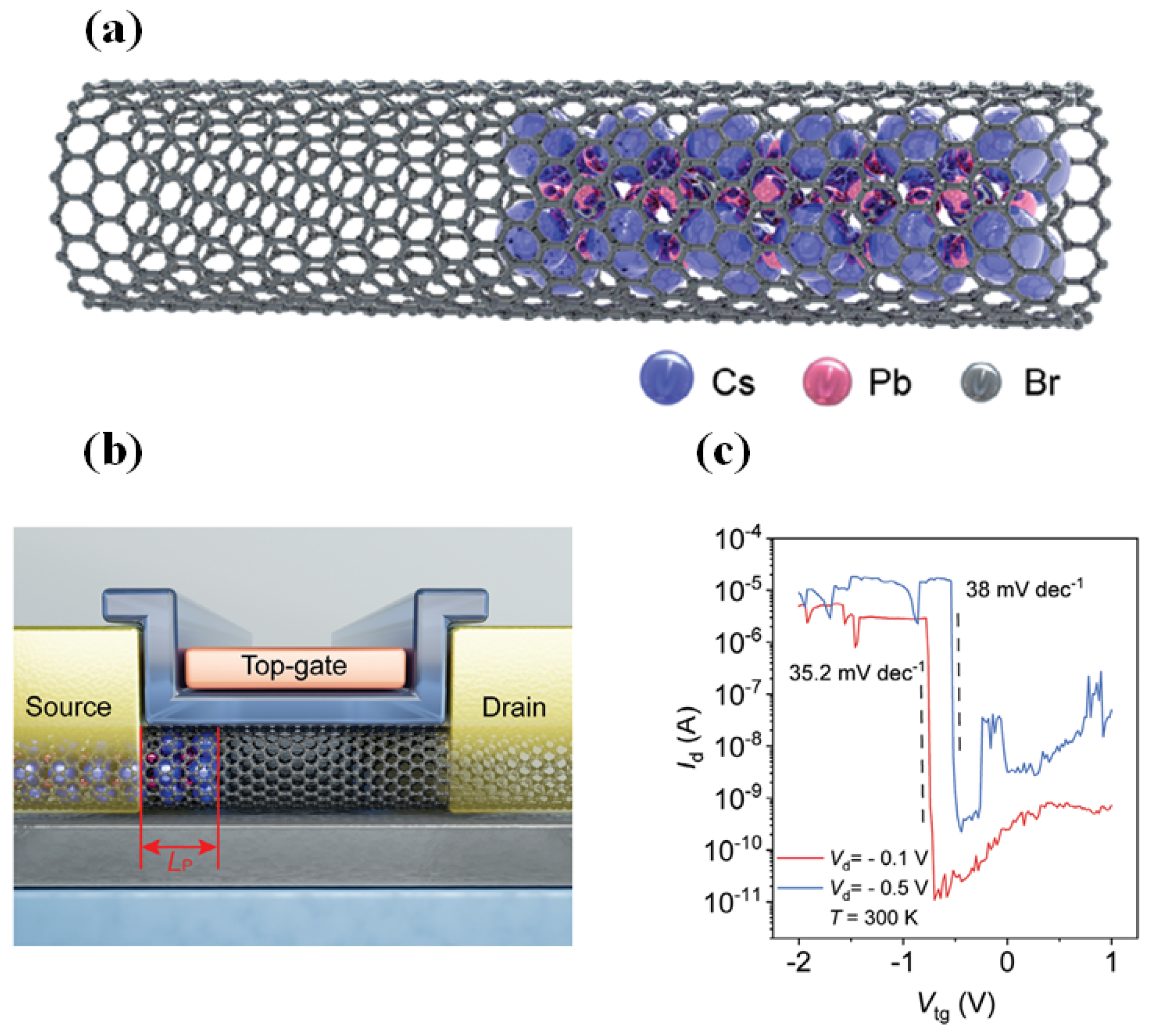
2.4. Carbon Nanotubes TFET

| Device Name | SS (mV/dec) | Ion (μA/μm) | Ion/Ioff | Vd (V) | Ref. |
|---|---|---|---|---|---|
| SOI Si-TFET | 52.8 | 12.1 | ∼2.2 × 10³ | 1.0 | [6] |
| Si/Ge DG TFET | ~50 | ~300 | - | - | [7] |
| Si Line Tunneling TFET | 69 | 40 | >107 | 1.0 | [18] |
| InGaAs TFET | 64 | 1.0 | 106 | - | [19] |
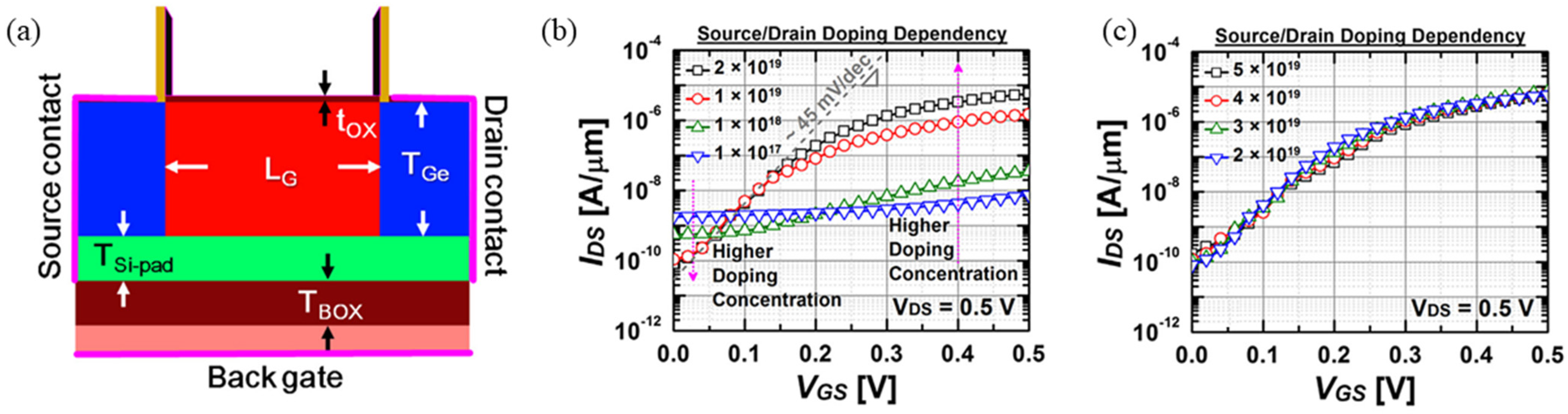
| InGaAs/GaAsSb TFET | 43 | - | - | 0.05 | [16] |
| InAs/GaSb NW-TFET | - | 5 × 10⁻⁵ (A/μm2) | - | 2.0 | [35] |
| WSe2/MoS2 TFET | 36 | 100 | 106 | −1.0 | [51] |
| Cr/hBN/MoS2 TFET | - | - | 5 × 10³ | - | [54] |
| Cr/hBN/MoS2/MoTe2 TFET | - | - | 6 × 10⁸ | −1.0 | [55] |
| WSe2/SnSe2 TFET | 37 | 1.5 | >106 | - | [50] |
| MoS2/Ge TFET | 46.4 | - | - | - | [13] |
| MoS2/Si TFET | 23 | - | >107 | - | [52] |
| InSe/Si TFET | 6.4 | 0.3 | - | −1.0 | [53] |
| BP RED-TFET | 170 | 0.6 | - | 0.8 | [56] |
| Nb-doped MoS2 TFET | 140 | - | - | 2.0 | [57] |
| BP Homojunction TFET | 23.7–24.0 | - | - | 0.6/0.7 | [15] |
| CNT Triple Gate TFET | 41 | 0.1 | - | - | [61] |
| CsPbBr3 CNT TFET | 35.2 | 4.94 | >105 | −0.1 | [63] |
3. Simulation Research Works on TFETs
| Device Name | SS (mV/dec) | Ion (μA/μm) | Ion/Ioff | Vd (V) | Ref. |
|---|---|---|---|---|---|
| NC-LTFET | 18.3 | 0.24 | - | - | [64] |
| S-TFET | 45 | - | 105 | 0.5 | [65] |
| SUTFET | 15.2 | 13.5 | 4.4 × 10⁶ | 0.5 | [14] |
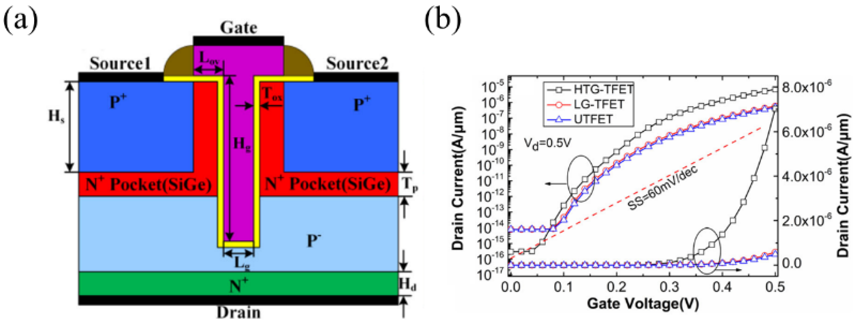
| HTG-TFET | 36.59 | 7.02 | - | 0.2 | [66] |
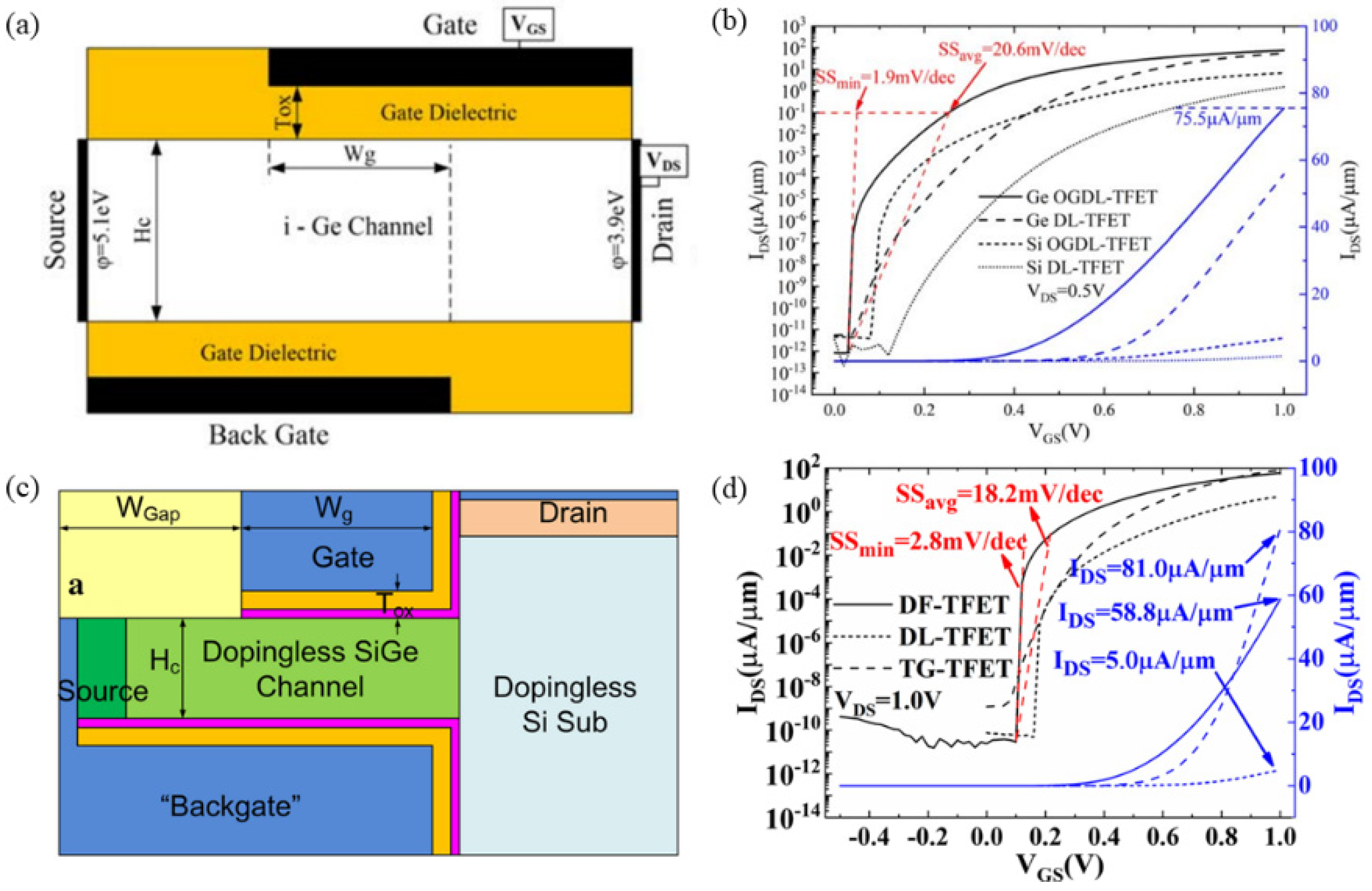
| OGDL-TFET | 20.6 | 75.5 | 9 × 10¹³ | 0.5 | [67] |
| DF-TFET | 18.2 | 58.8 | - | - | [68] |
| SNPJL-TFET | 20 | 54.3 | 1.45 × 10¹⁴ | 0.5 | [69] |
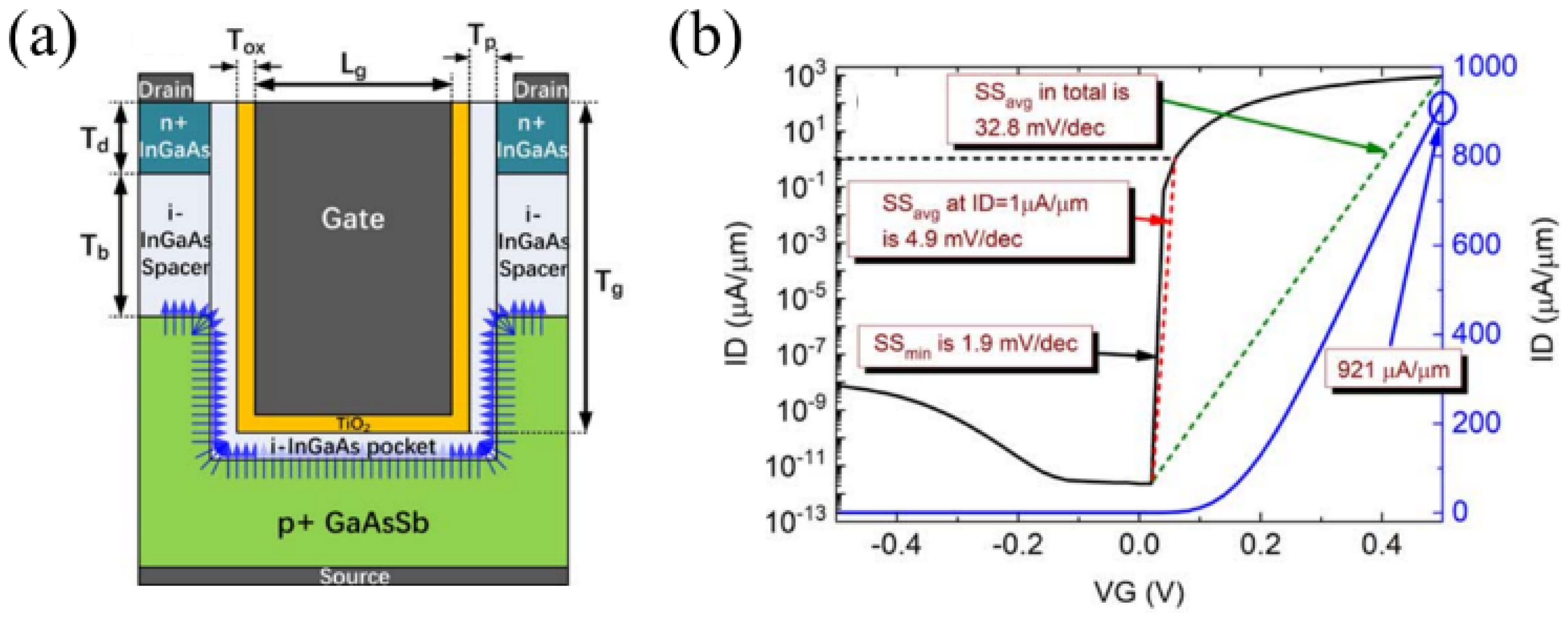
| QB-TFET | 4.9 | 921 | - | 0.5 | [17] |
3.1. p-n-i-n TFET
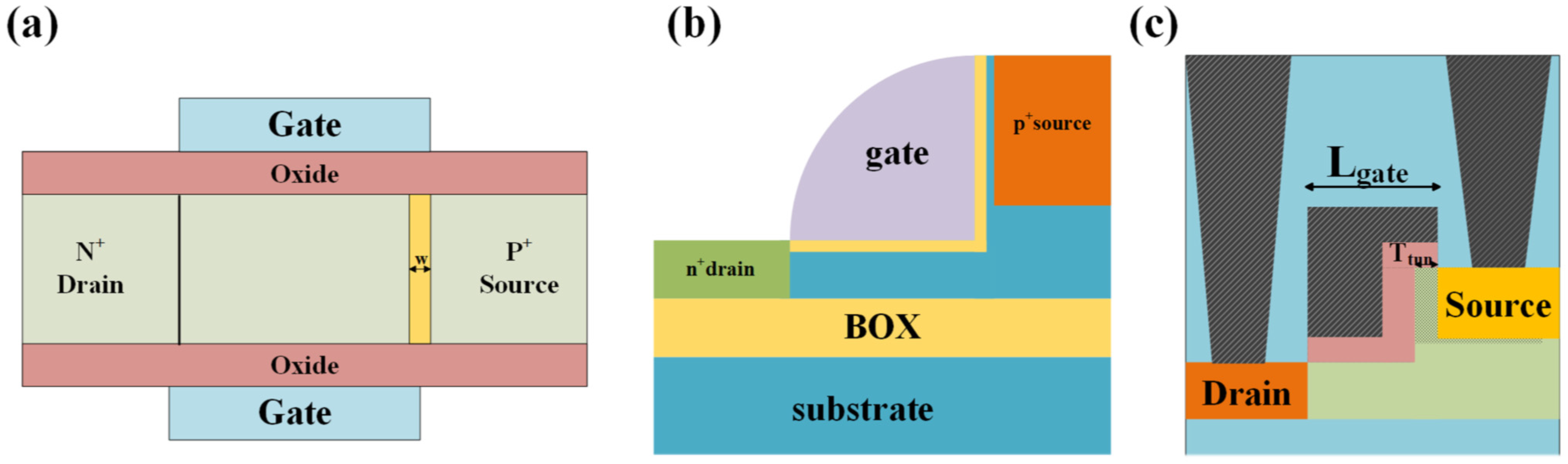
3.2. L-Shaped TFET
3.3. U-Shaped TFET
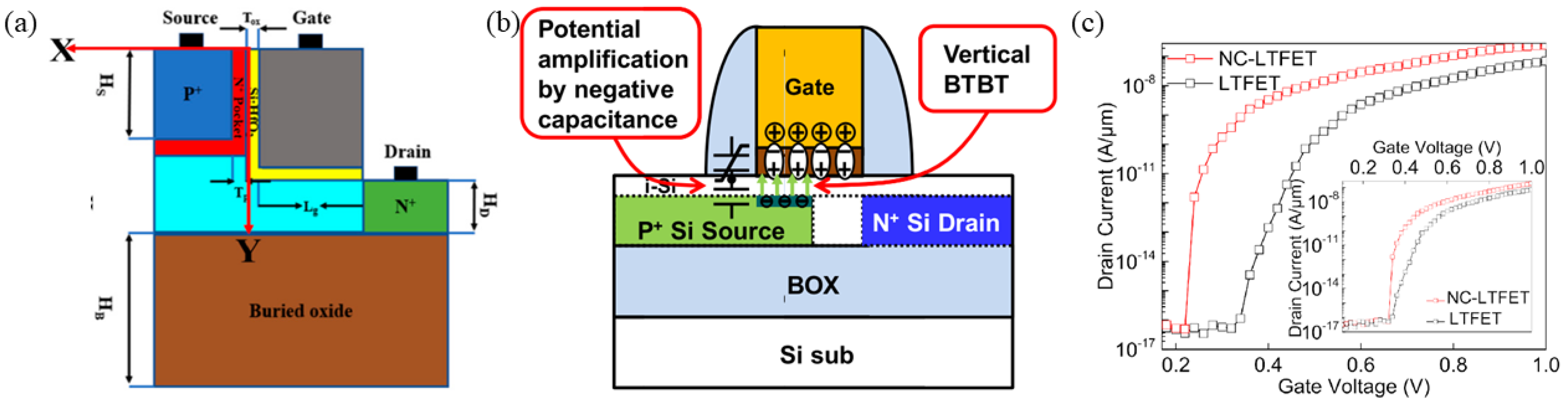
3.4. Symmetric Tunnel Field-Effect Transistor
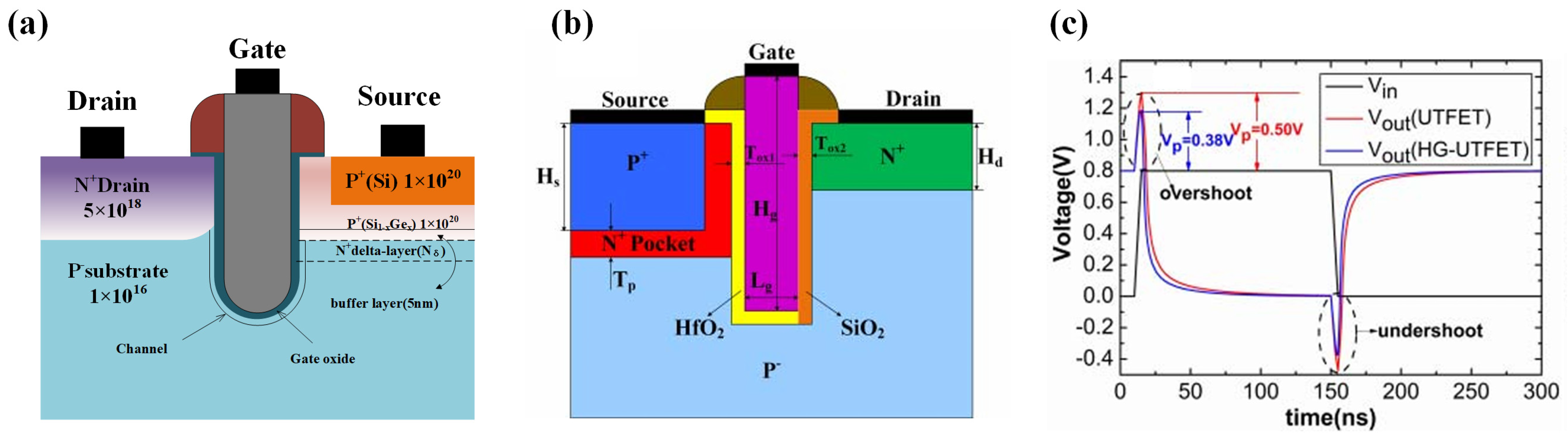
3.5. HTG-TFET
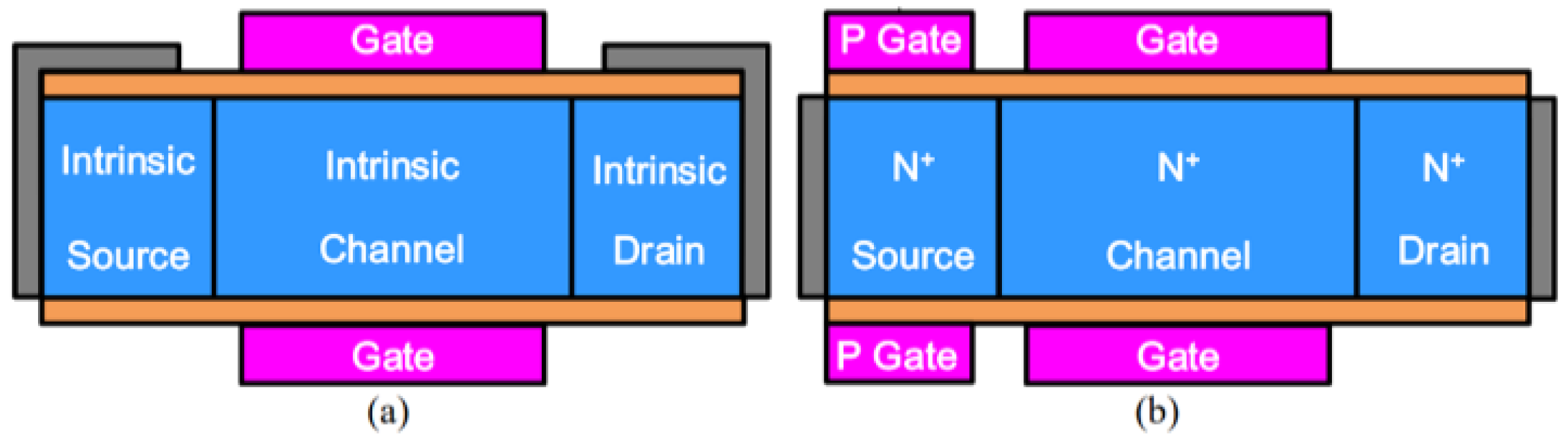
3.6. DL-TFET and JL-TFET
3.7. QB-TFET
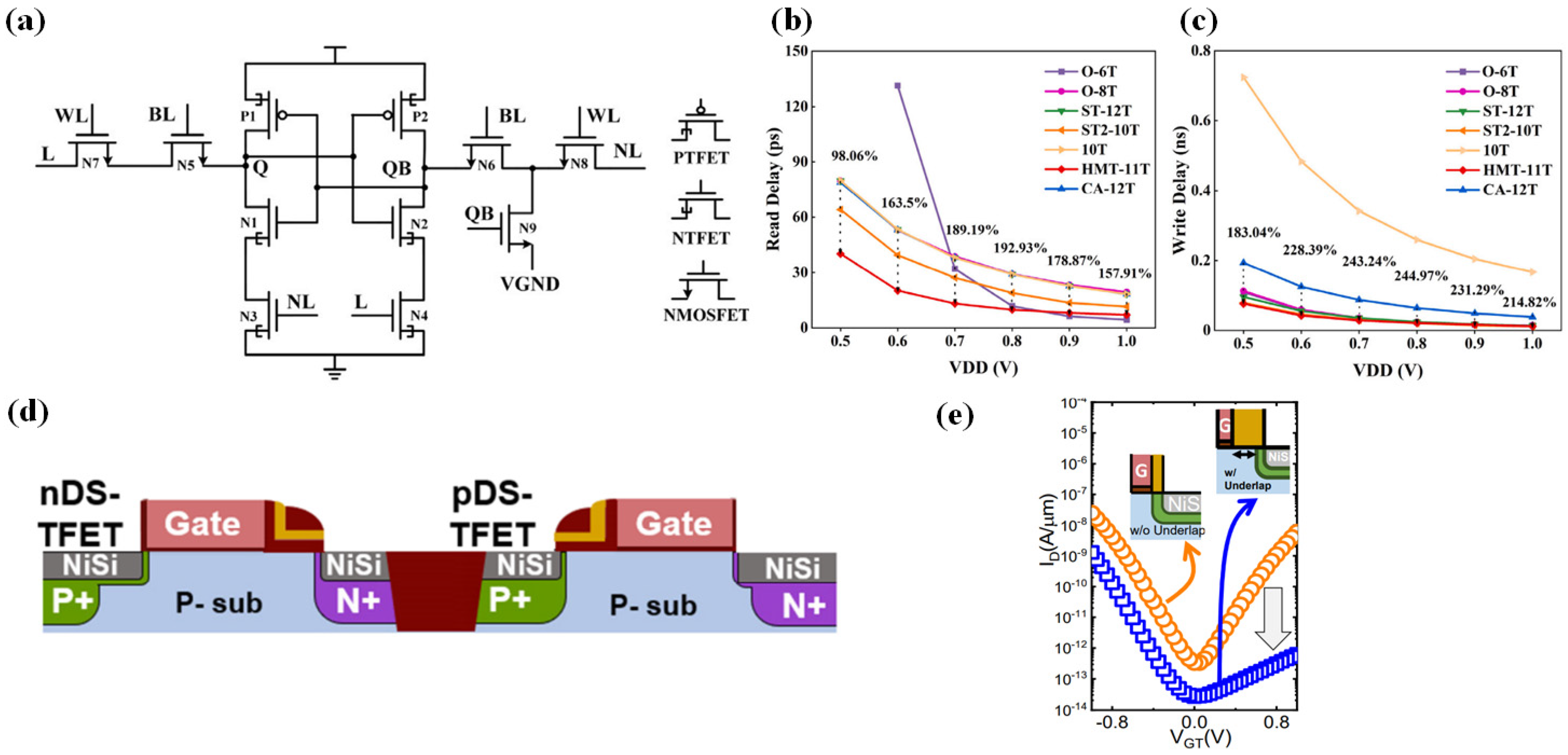
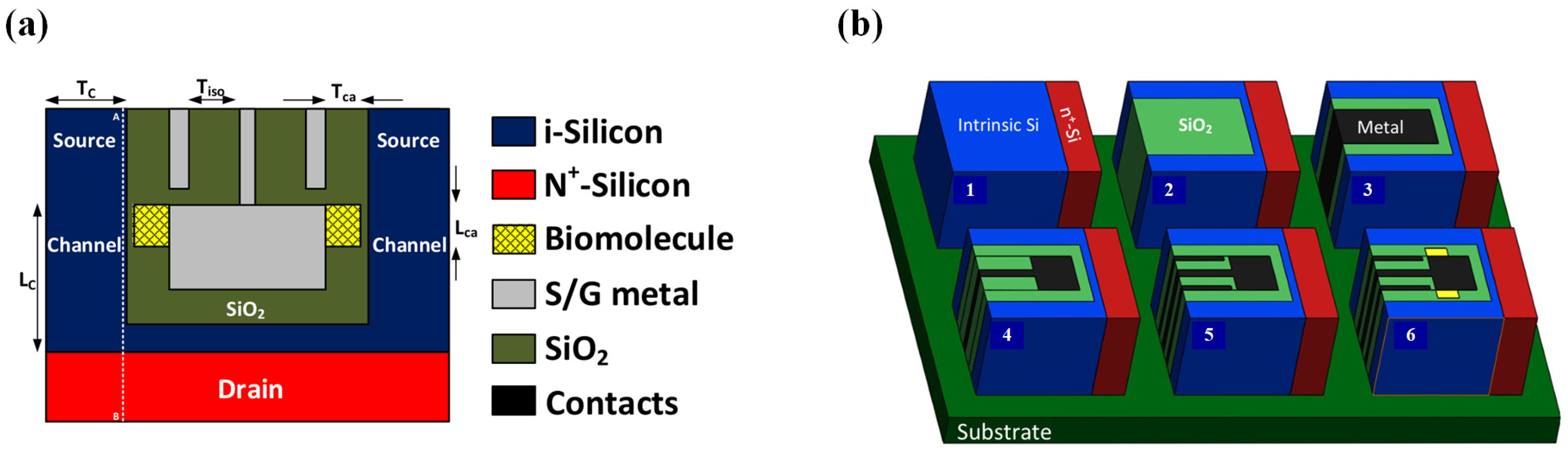
4. Applications of TFETs
5. Conclusions
Funding
Conflicts of Interest
References
- Tajalli, A.; Leblebici, Y. Design trade-offs in ultra-low-power digital nanoscale cmos. IEEE Trans. Circuits Syst. I Regul. Pap. 2011, 58, 2189–2200. [Google Scholar] [CrossRef]
- Franco, J.; Alian, A.; Vandooren, A.; Verhulst, A.S.; Linten, D.; Collaert, N.; Thean, A. Intrinsic robustness of tfet subthreshold swing to interface and oxide traps: A comparative pbti study of ingaas tfets and mosfets. IEEE Electron Device Lett. 2016, 37, 1055–1058. [Google Scholar] [CrossRef]
- Núñez, J.; Avedillo, M.J. Comparison of tfets and cmos using optimal design points for power–speed tradeoffs. IEEE Trans. Nanotechnol. 2016, 16, 83–89. [Google Scholar]
- Seabaugh, A.C.; Zhang, Q. Low-voltage tunnel transistors for beyond cmos logic. Proc. IEEE 2010, 98, 2095–2110. [Google Scholar] [CrossRef]
- Lin, Y.M.; Appenzeller, J.; Avouris, P. Novel carbon nanotube fet design with tunable polarity. In Proceedings of the IEDM Technical Digest. IEEE International Electron Devices Meeting, 2004, San Francisco, CA, USA, 13–15 December 2004. [Google Scholar]
- Choi, W.Y.; Park, B.G.; Lee, J.D.; Liu, T.J.K. Tunneling field-effect transistors (tfets) with subthreshold swing (ss) less than 60 mv/dec. IEEE Electron Device Lett. 2007, 28, 743–745. [Google Scholar] [CrossRef]
- Krishnamohan, T.; Kim, D.; Raghunathan, S.; Saraswat, K. Double-Gate Strained-Ge Heterostructure Tunneling FET (TFET) With record high drive currents and 60 mV/dec subthreshold slope. In Proceedings of the 2008 IEEE International Electron Devices Meeting, San Francisco, CA, USA, 15–17 December 2008. [Google Scholar]
- Cao, W.; Yao, C.J.; Jiao, G.F.; Huang, D.; Yu, H.Y.; Li, M.F. Improvement in reliability of tunneling field-effect transistor with p-n-i-n structure. IEEE Trans. Electron Devices 2011, 58, 2122–2126. [Google Scholar] [CrossRef]
- Kim, S.W.; Choi, W.Y.; Sun, M.C.; Kim, H.W.; Park, B.G. Design guideline of si-based l-shaped tunneling field-effect transistors. Jpn. J. Appl. Phys. 2012, 51, 501–504. [Google Scholar]
- Noguchi, M.; Kim, S.H.; Yokoyama, M.; Ji, S.M.; Ichikawa, O.; Osada, T. High ion/ioff and low subthreshold slope planar-type ingaas tunnel fets with zn-diffused source junctions. In Proceedings of the 2013 IEEE International Electron Devices Meeting, Washington, DC, USA, 9–11 December 2013. [Google Scholar]
- Kumar, M.J.; Janardhanan, S. Doping-less tunnel field effect transistor: Design and investigation. IEEE Trans. Electron Devices 2013, 60, 3285–3290. [Google Scholar] [CrossRef]
- Ghosh, B.; Akram, M.W. Junctionless tunnel field effect transistor. IEEE Electron Device Lett. 2013, 34, 584–586. [Google Scholar] [CrossRef]
- Sarkar, D.; Xie, X.; Liu, W.; Cao, W.; Kang, J.; Gong, Y.; Kraemer, S.; Ajayan, P.M.; Banerjee, K. A subthermionic tunnel field-effect transistor with an atomically thin channel. Nature 2015, 526, 91–95. [Google Scholar] [CrossRef]
- Chen, S.; Wang, S.; Liu, H.; Li, W.; Wang, Q.; Wang, X. Symmetric u-shaped gate tunnel field-effect transistor. IEEE Trans. Electron Devices 2017, 64, 1343–1349. [Google Scholar] [CrossRef]
- Kim, S.; Myeong, G.; Shin, W.; Lim, H.; Kim, B.; Jin, T.; Chang, S.; Watanabe, K.; Taniguchi, T.; Cho, S. Thickness-controlled black phosphorus tunnel field-effect transistor for low-power switches. Nat. Nanotechnol. 2020, 15, 203–206. [Google Scholar] [CrossRef] [PubMed]
- Convertino, C.; Zota, C.B.; Schmid, H.; Caimi, D.; Moselund, K.E. A hybrid iii–v tunnel fet and mosfet technology platform integrated on silicon. Nat. Electron. 2021, 4, 162–170. [Google Scholar] [CrossRef]
- Chen, S.; Wang, S.; Liu, H.; Han, T.; Zhang, H. A high performance trench gate tunneling field effect transistor based on quasi-broken gap energy band alignment heterojunction. Nanotechnology 2022, 33, 225205. [Google Scholar] [CrossRef]
- Cheng, W.; Liang, R.; Xu, G.; Yu, G.; Xu, J. Fabrication and characterization of a novel si line tunneling tfet with high drive current. IEEE J. Electron Devices Soc. 2020, 8, 336–340. [Google Scholar] [CrossRef]
- Noguchi, M.; Kim, S.; Yokoyama, M.; Ichikawa, O.; Osada, T.; Hata, M.; Takenaka, M.; Takagi, S. High ion/ioff and low subthreshold slope planar-type ingaas tunnel fets with zn-diffused source junctions. J. Appl. Phys. 2015, 118, 045712. [Google Scholar] [CrossRef]
- Singh, S.; Solay, L.R.; Anand, S.; Kumar, N.; Ranjan, R.; Singh, A. Implementation of Gate-All-Around Gate-Engineered Charge Plasma Nanowire FET-Based Common Source Amplifier. Micromachines 2023, 14, 1357. [Google Scholar] [CrossRef]
- Vishnupriyan, J.; Chayadevi, S.K.; Megala, V.; Karpagam, R. Design and qualitative analysis of 5-nm nanowire tfet with spacer engineering. J. Electron. Mater. 2023, 52, 2094–2099. [Google Scholar] [CrossRef]
- Dey, A.W.; Borg, B.M.; Ganjipour, B.; Ek, M.; Dick, K.A.; Lind, E.; Thelander, C.; Wernersson, L.E. High-current gasb/inas(sb) nanowire tunnel field-effect transistors. IEEE Electron Device Lett. 2013, 34, 211–213. [Google Scholar] [CrossRef]
- Iutzi, R.M.; Fitzgerald, E.A. Microstructure and conductance-slope of inas/gasb tunnel diodes. J. Appl. Phys. 2014, 115, 2095–2096. [Google Scholar] [CrossRef]
- Iutzi, R.M.; Fitzgerald, E.A. Defect and temperature dependence of tunneling in inas/gasb heterojunctions. Appl. Phys. Lett. 2015, 107, 133504. [Google Scholar] [CrossRef]
- Iutzi, R.M.; Fitzgerald, E.A. Conductance slope and curvature coefficient of ingaas/gaassb heterojunctions at varying band alignments and its implication on digital and analog applications. J. Appl. Phys. 2015, 118, 235702. [Google Scholar] [CrossRef]
- Zhang, X.B.; Ryou, J.H.; Dupuis, R.D.; Xu, C.; Mou, S.; Petschke, A.; Hsieh, K.C.; Chuang, S.L. Improved surface and structural properties of in as/ga sb superlattices on (001) gasb substrate by introducing an inassb layer at interfaces. Appl. Phys. Lett. 2007, 90, 1116. [Google Scholar]
- Booker, G.R.; Klipstein, P.C.; Lakrimi, M.; Lyapin, S.; Walker, P.J. Growth of inas/gasb strained layer superlattices. I. J. Cryst. Growth 1994, 145, 778–785. [Google Scholar] [CrossRef]
- Wang, S.; Wu, P.C.; Su, V.C.; Lai, Y.C.; Chen, M.K.; Kuo, H.Y.; Chen, B.H.; Chen, Y.H.; Huang, T.T.; Wang, J.H.; et al. A broadband achromatic metalens in the visible. Nat. Nanotechnol. 2018, 13, 227–232. [Google Scholar] [CrossRef] [PubMed]
- Huang, Y.; Ryou, J.; Dupuis, R.D.; Petschke, A.; Mandl, M.; Chuang, S. Inas/gasb type-ii superlattice structures and photodiodes grown by metalorganic chemical vapor deposition. Appl. Phys. Lett. 2010, 96, 2545. [Google Scholar] [CrossRef]
- Lackner, D.; Pitts, O.J.; Najmi, S.; Sandhu, P.; Kavanagh, K.L.; Yang, A.; Steger, M.; Thewalt, M.L.; Wang, Y.; McComb, D.W.; et al. Growth of inassb/inas mqws on gasb for mid-ir photodetector applications. J. Cryst. Growth 2009, 311, 3563–3567. [Google Scholar] [CrossRef]
- Zhu, Y.; Jain, N.; Vijayaraghavan, S.; Mohata, D.K.; Datta, S.; Lubyshev, D.; Fastenau, J.M.; Liu, W.K.; Monsegue, N.; Hudait, M.K. Role of inas and gaas terminated heterointerfaces at source/channel on the mixed as-sb staggered gap tunnel field effect transistor structures grown by molecular beam epitaxy. J. Appl. Phys. 2012, 112, 2568. [Google Scholar] [CrossRef]
- Zhu, Y.; Mohata, D.K.; Datta, S.; Hudait, M.K. Reliability studies on high-temperature operation of mixed as/sb staggered gap tunnel fet material and devices. IEEE Trans. Device Mater. Reliab. 2014, 14, 245–254. [Google Scholar] [CrossRef]
- Xie, Q.; Van Nostrand, J.E.; Brown, J.L.; Stutz, C.E. Arsenic for antimony exchange on gasb, its impacts on surface morphology, and interface structure. J. Appl. Phys. 1999, 86, 329–337. [Google Scholar] [CrossRef]
- Kaspi, R. Compositional abruptness at the inas-on-gasb interface: Optimizing growth by using the sb desorption signature. J. Cryst. Growth 1999, 201–202, 864–867. [Google Scholar] [CrossRef]
- Liu, J.S.; Clavel, M.; Pandey, R.; Datta, S.; Hudait, M.K. Heterogeneous integration of inas/gasb tunnel diode structure on silicon using 200 nm gaassb dislocation filtering buffer. AIP Adv. 2018, 8, 105108. [Google Scholar] [CrossRef]
- Zhao, X.; Vardi, A.; del Alamo, J.A. Sub-Thermal Subthreshold Characteristics in Top–Down InGaAs/InAs Heterojunction Vertical Nanowire Tunnel FETs. IEEE Electron Device Lett. 2017, 38, 855–858. [Google Scholar] [CrossRef]
- Vasen, T.; Ramvall, P.; Afzalian, A.; Doornbos, G.; Holland, M.; Thelander, C.; Dick, K.A.; Wernersson, L.E.; Passlack, M. Vertical gate-all-around nanowire gasb-inas core-shell n-type tunnel fets. Sci. Rep. 2019, 9, 202. [Google Scholar] [CrossRef]
- Solay, L.R.; Kumar, N.; Amin, S.I.; Kumar, P.; Anand, S. Design and performance analysis of gate-all-around negative capacitance dopingless nanowire tunnel field effect transistor. Semicond. Sci. Technol. 2022, 37, 115001. [Google Scholar] [CrossRef]
- Arun, A.V.; Sreelekshmi, P.S.; Jacob, J. Implementation of an Efficient Charge Pump using Gate All Around Nanowire TFET for Energy Harvesting Applications. In Proceedings of the 2024 28th International Symposium on VLSI Design and Test (VDAT), Vellore, India, 1–3 September 2024. [Google Scholar]
- Zhu, Z.; Persson, A.E.O.; Wernersson, L. Reconfigurable signal modulation in a ferroelectric tunnel field-effect transistor. Nat. Commun. 2023, 14, 2530. [Google Scholar] [CrossRef] [PubMed]
- Kaniselvan, M.; Yoon, Y. Strain-tuning ptse2 for high on-current lateral tunnel field-effect transistors. Appl. Phys. Lett. 2021, 119, 073102. [Google Scholar] [CrossRef]
- Nakamura, K.; Nagamura, N.; Ueno, K.; Taniguchi, T.; Nagashio, K. All 2D heterostructure tunnel field effect transistors: Impact of band alignment and heterointerface quality. ACS Appl. Mater. Interfaces 2020, 12, 51598–51606. [Google Scholar] [CrossRef]
- Iordanidou, K.; Mitra, R.; Shetty, N.; Lara-Avila, S.; Dash, S.; Kubatkin, S.; Wiktor, J. Electric field and strain tuning of 2D semiconductor van der waals heterostructures for tunnel field-effect transistors. ACS Appl. Mater. Interfaces 2022, 15, 1762–1771. [Google Scholar] [CrossRef]
- Lemme, M.C.; Akinwande, D.; Huyghebaert, C.; Stampfer, C. 2D materials for future heterogeneous electronics. Nat. Commun. 2022, 13, 1392. [Google Scholar] [CrossRef]
- Pande, G.; Siao, J.Y.; Chen, W.L.; Lee, C.J.; Sankar, R.; Chang, Y.M.; Chen, C.D.; Chang, W.H.; Chou, F.C.; Lin, M.T. Ultralow schottky barriers in hexagonal boron nitride-encapsulated monolayer WSe2 tunnel field-effect transistors. ACS Appl. Mater. Interfaces 2020, 12, 18667–18673. [Google Scholar] [CrossRef]
- Zhou, W.X.; Chen, K.Q. First-principles determination of ultralow thermal conductivity of monolayer wse2. Sci. Rep. 2015, 5, 15070. [Google Scholar] [CrossRef]
- Roy, T.; Tosun, M.; Cao, X.; Fang, H.; Javey, A. Dual-gated MoS2/WSe2 van der waals tunnel diodes and transistors. ACS Nano 2015, 9, 2071–2079. [Google Scholar] [CrossRef]
- Yan, R.; Fathipour, S.; Han, Y.; Song, B.; Xiao, S.; Li, M.; Ma, N.; Protasenko, V.; Muller, D.A.; Jena, D.; et al. Esaki diodes in van der waals heterojunctions with broken-gap energy band alignment. Nano Lett. 2015, 15, 5791–5798. [Google Scholar] [CrossRef]
- Roy, T.; Tosun, M.; Hettick, M.; Ahn, G.H.; Hu, C.; Javey, A. 2D-2D tunneling field-effect transistors using WSe2/SnSe2 heterostructures. Appl. Phys. Lett. 2016, 108, 083111. [Google Scholar] [CrossRef]
- Yan, X.; Liu, C.; Li, C.; Bao, W.; Zhou, P. Tunable SnSe2/WSe2 heterostructure tunneling field effect transistor. Small 2017, 13, 68. [Google Scholar] [CrossRef] [PubMed]
- Jeon, H.B.; Shin, G.H.; Lee, K.J.; Choi, S.Y. Vertical-tunneling field-effect transistor based on WSe2-MoS2 heterostructure with ion gel dielectric. Adv. Electron. Mater. 2020, 6, 2000091. [Google Scholar] [CrossRef]
- Shin, G.; Koo, B.; Park, H.; Woo, Y.; Lee, J.; Choi, S. Vertical-tunnel field-effect transistor based on a Silicon-Mos2 three-dimensional-two-dimensional heterostructure. ACS Appl. Mater. Interfaces 2018, 10, 40212–40218. [Google Scholar] [CrossRef] [PubMed]
- Miao, J.; Leblanc, C.; Wang, J.; Gu, Y.; Liu, X.; Song, B.; Zhang, H.; Krylyuk, S.; Hu, W.; Davydov, A.V.; et al. Heterojunction tunnel triodes based on two-dimensional metal selenide and three-dimensional silicon. Nat. Electron. 2022, 5, 744–751. [Google Scholar] [CrossRef]
- Cheng, R.; Wang, F.; Yin, L.; Xu, K.; Ahmed Shifa, T.; Wen, Y.; Zhan, X.; Li, J.; Jiang, C.; Wang, Z.; et al. Multifunctional tunneling devices based on graphene/h-BN/MoSe2 van der Waals heterostructures. Appl. Phys. Lett. 2017, 110, 173507. [Google Scholar] [CrossRef]
- Cheng, R.; Wang, F.; Yin, L.; Wang, Z.; Wen, Y.; Shifa, T.A.; He, J. High-performance, multifunctional devices based on asymmetric van der Waals heterostructures. Nat. Electron. 2018, 1, 356–361. [Google Scholar] [CrossRef]
- Wu, P.; Ameen, T.; Zhang, H.; Bendersky, L.A.; Ilatikhameneh, H.; Klimeck, G.; Rahman, R.; Davydov, A.V.; Appenzeller, J. Complementary black phosphorus tunneling field-effect transistors. ACS Nano 2019, 13, 377–385. [Google Scholar] [CrossRef]
- Fukui, T.; Nishimura, T.; Miyata, Y.; Ueno, K.; Taniguchi, T.; Watanabe, K.; Nagashio, K. Single-Gate MoS2 Tunnel FET with a Thickness-Modulated Homojunction. ACS Appl. Mater. Interfaces 2024, 16, 8993–9001. [Google Scholar] [CrossRef]
- Tran, V.; Soklaski, R.; Liang, Y.; Yang, L. Layer-controlled band gap and anisotropic excitons in few-layer black phosphorus. Phys. Rev. B 2014, 89, 817–824. [Google Scholar] [CrossRef]
- Ahmadchally, A.A.; Gholipour, M. Investigation of 6-armchair graphene nanoribbon tunnel fets. J. Comput. Electron. 2021, 20, 1114–1124. [Google Scholar] [CrossRef]
- Appenzeller, J.; Lin, Y.M.; Knoch, J.; Avouris, P. Band-to-band tunneling in carbon nanotube field-effect transistors. Phys. Rev. Lett. 2004, 93, 196805. [Google Scholar] [CrossRef] [PubMed]
- Pang, C.-S.; Han, S.-J.; Chen, Z. Steep slope carbon nanotube tunneling field-effect transistor. Carbon 2021, 180, 237–243. [Google Scholar] [CrossRef]
- Zhou, C.; Kong, J.; Yenilmez, E.; Dai, H. Modulated Chemical Doping of Individual Carbon Nanotubes. Science 2000, 290, 1552–1555. [Google Scholar] [CrossRef]
- Zhu, M.; Yin, H.; Cao, J.; Xu, L.; Lu, P.; Liu, Y.; Ding, L.; Fan, C.; Liu, H.; Zhang, Y.; et al. Inner Doping of Carbon Nanotubes with Perovskites for Ultralow Power Transistors. Adv. Mater. 2024, 36, 2403743. [Google Scholar] [CrossRef] [PubMed]
- Zhang, H.; Chen, S.; Liu, H.; Wang, S.; Wang, D.; Fan, X.; Chong, C.; Yin, C.; Gao, T. Polarization Gradient Effect of Negative Capacitance LTFET. Micromachines 2022, 13, 344. [Google Scholar] [CrossRef] [PubMed]
- Nam, H.; Cho, M.H.; Shin, C. Symmetric tunnel field-effect transistor (s-tfet). Curr. Appl. Phys. 2015, 15, 71–77. [Google Scholar] [CrossRef]
- Li, W.; Liu, H.; Wang, S.; Chen, S.; Yang, Z. Design of high performance si/sige heterojunction tunneling fets with a t-shaped gate. Nanoscale Res. Lett. 2017, 12, 198. [Google Scholar] [CrossRef]
- Chen, S.; Liu, H.; Wang, S.; Han, T.; Li, W.; Wang, X. A novel Ge based overlapping gate dopingless tunnel FET with high performance. Jpn. J. Appl. Phys. 2019, 58, 100902. [Google Scholar] [CrossRef]
- Chen, S.; Wang, S.; Liu, H.; Han, T.; Chong, C. A novel dopingless fin-shaped sige channel tfet with improved performance. Nanoscale Res. Lett. 2020, 15, 202. [Google Scholar] [CrossRef] [PubMed]
- Hussain, S.; Mustakim, N.; Hasan, M.; Saha, J.K. Performance enhancement of charge plasma-based junctionless TFET (JL-TFET) using stimulated n-pocket and heterogeneous gate dielectric. Nanotechnology 2021, 32, 335206. [Google Scholar] [CrossRef] [PubMed]
- Sze, S.M. Physics of Semiconductor Devices, 3rd ed.; John Wiley & Sons: Hoboken, NJ, USA, 2006; p. 422. [Google Scholar]
- Yu, T. Massachusetts Institute of Technology. InGaAs/GaAsSb Quantum-Well Tunnel-FETs for Ultra-Low Power Applications. Ph.D. Thesis, Massachusetts Institute of Technology, Cambridge, MA, USA, 2016. [Google Scholar]
- Kim, S.H.; Agarwal, S.; Jacobson, Z.A.; Matheu, P.; Hu, C.; Liu, T.J.K. Tunnel field effect transistor with raised germanium source. IEEE Electron Device Lett. 2010, 31, 1107–1109. [Google Scholar] [CrossRef]
- Kim, S.W.; Kim, J.H.; Liu, T.J.K.; Choi, W.Y.; Park, B.G. Demonstration of l-shaped tunnel field-effect transistors. IEEE Trans. Electron Devices 2015, 63, 1774–1778. [Google Scholar] [CrossRef]
- Chander, S.; Sinha, S.K.; Chaudhary, R.; Singh, A. Ge-source based l-shaped tunnel field effect transistor for low power switching application. Silicon 2022, 14, 7435–7448. [Google Scholar] [CrossRef]
- Kobayashi, M.; Jang, K.; Ueyama, N.; Hiramoto, T. Negative capacitance for boosting tunnel fet performance. IEEE Trans. Nanotechnol. 2017, 16, 253–258. [Google Scholar] [CrossRef]
- Bscke, T.S.; Miiller, J.; Brauhaus, D.; Schroder, U.; Bottger, U. Ferroelectricity in hafnium oxide thin films. Appl. Phys. Lett. 2011, 99, 5397. [Google Scholar] [CrossRef]
- Wang, W.; Wang, P.F.; Zhang, C.M.; Lin, X. Design of u-shape channel tunnel fets with sige source regions. IEEE Trans. Electron Devices 2013, 61, 193–197. [Google Scholar] [CrossRef]
- Wang, W.; Zang, S.G.; Lin, X.; Liu, X.Y.; Zhang, D.W. A novel recessed-channel tu nneling fet design with boosted drive current and suppressed leakage current. In Proceedings of the 2012 IEEE 11th International Conference on Solid-State and Integrated Circuit Technology, Xi’an, China, 29 October–1 November 2012. [Google Scholar]
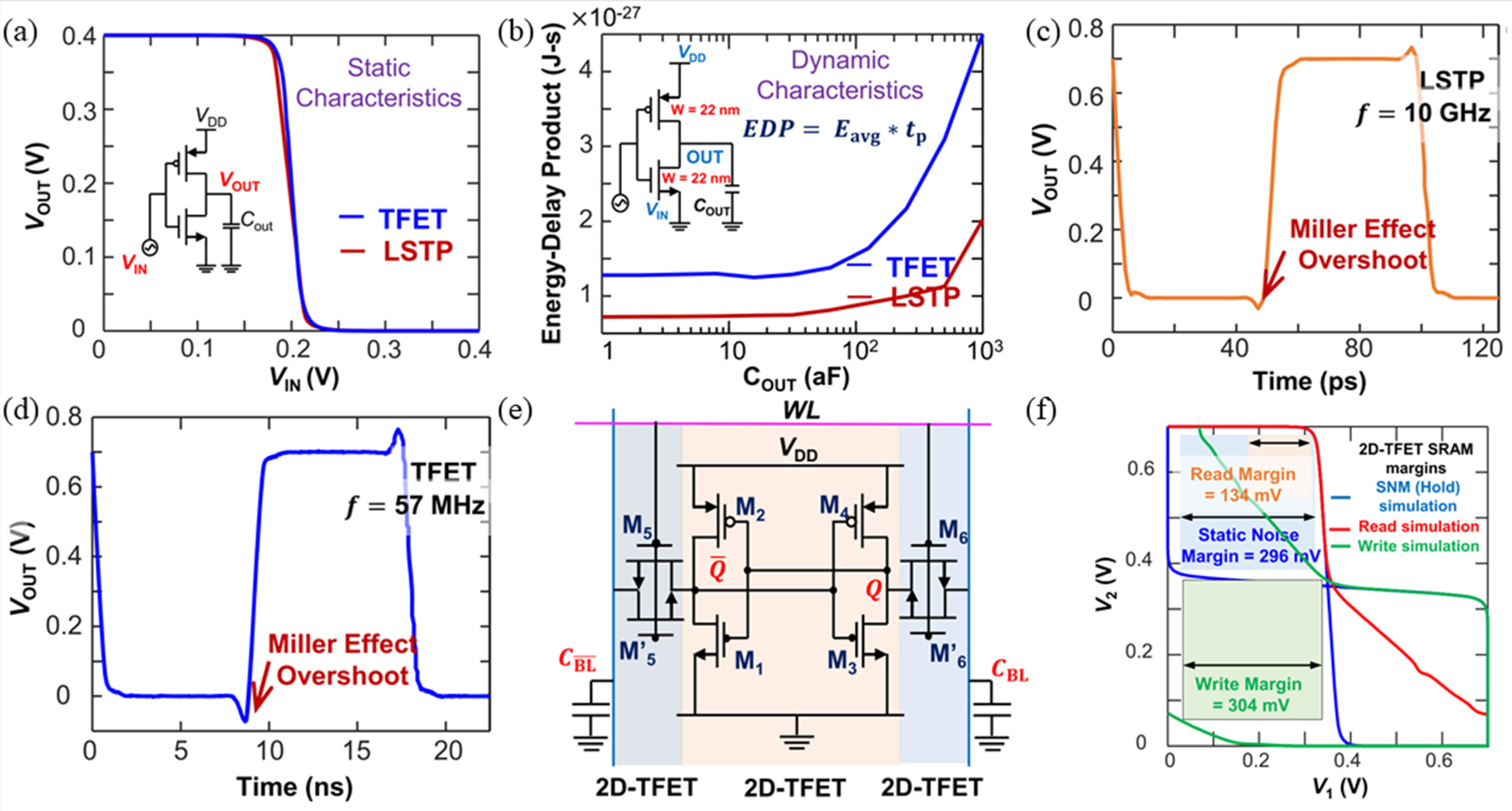
- Li, W.; Liu, H.; Wang, S.; Chen, S. Reduced miller capacitance in u-shaped channel tunneling fet by introducing heterogeneous gate dielectric. IEEE Electron Device Lett. 2017, 38, 403–406. [Google Scholar] [CrossRef]
- Krenik, W.R.; Izzi, L.J. Output Buffer Circuits with Controlled Miller Effect Capacitance. United. States Patent US 5,274,284, 28 December 1993. [Google Scholar]
- Israelsohn, J. Miller on edge: The role of miller capacitance in nonlinear circuits. EDN 2007. Available online: https://www.edn.com/miller-on-edge-the-role-of-miller-capacitance-in-nonlinear-circuits/ (accessed on 25 June 2025).
- Jiang, C.; Wu, D.D. Asymmetric S/D Structure to Improve Transistor Performance by Reducing Miller Capacitance. U.S. Patent 5,925,914, 20 July 1999. [Google Scholar]
- Mookerjea, S.; Krishnan, R.; Datta, S.; Narayanan, V. On enhanced miller capacitance effect in interband tunnel transistors. IEEE Electron Device Lett. 2009, 30, 1102–1104. [Google Scholar] [CrossRef]
- Mookerjea, S.; Krishnan, R.; Datta, S.; Narayanan, V. Effective capacitance and drive current for tunnel fet (tfet) cv/i estimation. IEEE Trans. Electron Devices 2009, 56, 2092–2098. [Google Scholar] [CrossRef]
- Yang, Y.; Tong, X.; Yang, L.T.; Guo, P.F.; Fan, L.; Yeo, Y.C. Tunneling field-effect transistor: Capacitance components and modeling. IEEE Electron Device Lett. 2010, 31, 752–754. [Google Scholar] [CrossRef]
- Elmasry, M.I. Capacitance calculations in mosfet vlsi. Electron Device Lett. IEEE 1982, 3, 6–7. [Google Scholar] [CrossRef]
- Upasana Narang, R.; Gupta, M.; Saxena, M. Simulation study for dual material gate hetero-dielectric tfet: Static performance analysis for analog applications. In Proceedings of the 2013 Annual IEEE India Conference (INDICON), Mumbai, India, 13–15 December 2013. [Google Scholar]
- Goswami, R.; Bhowmick, B. Hetero-gate-dielectric gate-drain underlap nanoscale tfet with a δp+ Si1−xGex layer at source-channel tunnel junction. In Proceedings of the 2014 International Conference on Green Computing Communication and Electrical Engineering (ICGCCEE), Coimbatore, India, 6–8 March 2014. [Google Scholar]
- Paul, D.J.; Abdullah-Al-Kaiser, M.; Islam, M.S.; Khosru, Q.D.M. Fringing-field-based 2-D analytical model for a gate-underlap double-gate TFET. J. Comput. Electron. 2018, 17, 1567–1577. [Google Scholar] [CrossRef]
- Ankur, B.; Nandakishor, Y.; Prasad, S.A.; Kumar, V.S. Analog/rf characteristics of a 3D-cyl underlap gaa-tfet based on a ge source using fringing-field engineering for low-power applications. J. Comput. Electron. 2018, 17, 1650–1657. [Google Scholar]
- Singh, G.; Amin, S.I.; Anand, S.; Sarin, R.K. Design of si0.5ge0.5 based tunnel field effect transistor and its performance evaluation. Superlattices Microstruct. 2016, 92, 143–156. [Google Scholar] [CrossRef]
- Damrongplasit, N.; Kim, S.H.; Liu, T.J.K. Study of random dopant fluctuation induced variability in the raised-ge-source TFET. Electron Device Lett. 2013, 34, 184–186. [Google Scholar] [CrossRef]
- Damrongplasit, N.; Kim, S.H.; Shin, C.; Liu, T.J. Impact of gate line-edge roughness (ler) versus random dopant fluctuations (rdf) on germanium-source tunnel fet performance. IEEE Trans. Nanotechnol. 2013, 12, 1061–1067. [Google Scholar] [CrossRef]
- Damrongplasit, N.; Shin, C.; Kim, S.H.; Vega, R.A.; King Liu, T.J. Study of random dopant fluctuation effects in germanium-source tunnel fets. IEEE Trans. Electron Devices 2011, 58, 3541–3548. [Google Scholar] [CrossRef]
- Anand, S.; Sarin, R.K. Hetero-material gate doping-less tunnel fet and its misalignment effects on analog/rf parameters. J. Electron. Mater. 2018, 47, 2988–2996. [Google Scholar] [CrossRef]
- Yadav, D.S.; Verma, A.; Sharma, D.; Tirkey, S.; Raad, B.R. Comparative investigation of novel hetero gate dielectric and drain engineered charge plasma tfet for improved dc and rf performance. Superlattices Microstruct. 2017, 111, 123–133. [Google Scholar] [CrossRef]
- Sharma, S.; Basu, R.; Kaur, B. Temperature Analysis of a Dopingless TFET Considering Interface Trap Charges for Enhanced Reliability. IEEE Trans. Electron Devices 2022, 69, 2692–2697. [Google Scholar] [CrossRef]
- Aghandeh, H.; Ziabari, S.A. Gate engineered heterostructure junctionless tfet with gaussian doping profile for ambipolar suppression and electrical performance improvement. Superlattices Microstruct. 2017, 111, 103–114. [Google Scholar] [CrossRef]
- Singh, D.; Pandey, S.; Nigam, K.; Sharma, D.; Yadav, D.S.; Kondekar, P. A charge-plasma-based dielectric-modulated junctionless tfet for biosensor label-free detection. IEEE Trans. Electron Devices 2016, 64, 271–278. [Google Scholar] [CrossRef]
- Gupta, S.; Nigam, K.; Pandey, S.; Sharma, D.; Kondekar, P.N. Effect of interface trap charges on performance variation of heterogeneous gate dielectric junctionless-tfet. IEEE Trans. Electron Devices 2017, 64, 4731–4737. [Google Scholar] [CrossRef]
- Pal, A.; Chai, Z.; Jiang, J.; Cao, W.; Davies, M.; De, V.; Banerjee, K. An ultra energy-efficient hardware platform for neuromorphic computing enabled by 2D-tmd tunnel-fets. Nat. Commun. 2024, 15, 3392. [Google Scholar] [CrossRef] [PubMed]
- Lu, W.; Wang, C.; Hu, W.; Dai, C.; Peng, C.; Lin, Z.; Wu, X. Hybrid MOSFET-TFET 11T SRAM cell with high write speed and free half-selected disturbance. Microelectron. J. 2025, 156, 106498. [Google Scholar] [CrossRef]
- Wang, K.; Huang, Q.; Wu, Y.; Ren, Y.; Wei, R.; Wang, Z.; Yang, L.; Zhang, F.; Geng, K.; Li, Y.; et al. A Novel Energy-Efficient Salicide-Enhanced Tunnel Device Technology Based on 300mm Foundry Platform Towards AIoT Applications. arXiv 2024, arXiv:2410.12390. [Google Scholar]
- Feng, G.; Liu, Y.; Zhu, Q.; Feng, Z.; Luo, S.; Qin, C.; Chen, L.; Xu, Y.; Wang, H.; Zubair, M.; et al. Giant tunnel electroresistance through a Van der Waals junction by external ferroelectric polarization. Nat. Commun. 2024, 15, 9701. [Google Scholar] [CrossRef]
- Cherik, I.C.; Mohammadi, S. Impact of trap-related non-idealities on the performance of a novel tfet-based biosensor with dual doping-less tunneling junction. Sci. Rep. 2023, 13, 11495. [Google Scholar] [CrossRef]
- Krsihna, B.V.; Chowdary, G.A.; Ravi, S.; Reddy, K.V.; Kavitha, K.R.; Panigrahy, A.K.; Prakash, M.D. Tunnel field effect transistor design and analysis for biosensing applications. Silicon 2022, 14, 10893–10899. [Google Scholar] [CrossRef]
- Anam, A.; Anand, S.; Amin, S.I. Design and Performance Analysis of Tunnel Field Effect Transistor With Buried Strained Si1−xGex Source Structure Based Biosensor for Sensitivity Enhancement. IEEE Sens. J. 2020, 20, 13178–13185. [Google Scholar] [CrossRef]
- Dwivedi, P.; Singh, R.; Sengar, B.S.; Kumar, A.; Garg, V. A New Simulation Approach of Transient Response to Enhance the Selectivity and Sensitivity in Tunneling Field Effect Transistor-Based Biosensor. IEEE Sens. J. 2021, 21, 3201–3209. [Google Scholar] [CrossRef]
- Kumar, P.; Sharma, S.K.; BalwinderRaj. Comparative analysis of nanowire tunnel field effect transistor for biosensor applications. Silicon 2021, 13, 4067–4074. [Google Scholar] [CrossRef]
- Gayduchenko, I.; Xu, S.G.; Alymov, G.; Moskotin, M.; Bandurin, D.A. Tunnel field-effect transistors for sensitive terahertz detection. Nat. Commun. 2021, 12, 543. [Google Scholar] [CrossRef]
- Singh, P.; Raman, A.; Yadav, D.S.; Kumar, N.; Dixit, A.; Ansari, H.R. Ultra thin finger-like source region-based tfet: Temperature sensor. IEEE Sens. Lett. 2024, 8, 2501104. [Google Scholar] [CrossRef]
- Nigam, K.; Pandey, S.; Kondekar, P.N.; Sharma, D. Temperature sensitivity analysis of polarity controlled electrically doped hetero-tfet. In Proceedings of the 2016 12th Conference on Ph. D. Research in Microelectronics and Electronics (PRIME) 2016, Lisbon, Portugal, 27–30 June 2016. [Google Scholar]
- Yousf, N.; Anam, A.; Rasool, Z.; Amin, S.I. Ultralow-Power DST-TFET pH Sensor Exceeding the Nernst Limit with Influence of Temperature on Sensitivity. ACS Appl. Bio Mater. 2024, 7, 4562–4572. [Google Scholar] [CrossRef]
- Singh, S.; Verma, A.; Singh, J.; Wadhwa, G. Investigation of n + SiGe gate stacked VTFET based on dopingless charge plasma for gas sensing application. Silicon 2022, 14, 6205–6218. [Google Scholar] [CrossRef]
- Ghosh, S.; Rajan, L.; Varghese, A. Junctionfree Gate Stacked Vertical TFET Hydrogen Sensor at Room Temperature. IEEE Trans. Nanotechnol. 2022, 21, 655–662. [Google Scholar] [CrossRef]
- Esseni, D.; Pala, M.; Palestri, P.; Alper, C.; Rollo, T. A review of selected topics in physics based modeling for tunnel field-effect transistors. Semicond. Sci. Technol. 2017, 32, 083005. [Google Scholar] [CrossRef]
- Yin, L.; Cheng, R.; Ding, J.; Jiang, J.; Hou, Y.; Feng, X.; Wen, Y.; He, J. Two-Dimensional Semiconductors and Transistors for Future Integrated Circuits. ACS Nano 2024, 18, 7739–7768. [Google Scholar] [CrossRef]
- Noyce, S.G.; Doherty, J.L.; Cheng, Z.; Han, H.; Bowen, S.; Franklin, A.D. Electronic Stability of Carbon Nanotube Transistors Under Long-Term Bias Stress. Nano Lett. 2019, 19, 1460–1466. [Google Scholar] [CrossRef]
- Rendón, M.; Cao, C.; Landázuri, K.; Garzón, E.; Prócel, L.M.; Taco, R. Performance Benchmarking of TFET and FinFET Digital Circuits from a Synthesis-Based Perspective. Electronics 2022, 11, 632. [Google Scholar] [CrossRef]
- Majumdar, K.; Bhat, N.; Majhi, P.; Jammy, R. Effects of Parasitics and Interface Traps on Ballistic Nanowire FET in the Ultimate Quantum Capacitance Limit. IEEE Trans. Electron Devices 2010, 57, 2264–2273. [Google Scholar] [CrossRef]


Disclaimer/Publisher’s Note: The statements, opinions and data contained in all publications are solely those of the individual author(s) and contributor(s) and not of MDPI and/or the editor(s). MDPI and/or the editor(s) disclaim responsibility for any injury to people or property resulting from any ideas, methods, instructions or products referred to in the content. |
© 2025 by the authors. Licensee MDPI, Basel, Switzerland. This article is an open access article distributed under the terms and conditions of the Creative Commons Attribution (CC BY) license (https://creativecommons.org/licenses/by/4.0/).
Share and Cite
Chen, S.; An, Y.; Wang, S.; Liu, H. A Review of Tunnel Field-Effect Transistors: Materials, Structures, and Applications. Micromachines 2025, 16, 881. https://doi.org/10.3390/mi16080881
Chen S, An Y, Wang S, Liu H. A Review of Tunnel Field-Effect Transistors: Materials, Structures, and Applications. Micromachines. 2025; 16(8):881. https://doi.org/10.3390/mi16080881
Chicago/Turabian StyleChen, Shupeng, Yourui An, Shulong Wang, and Hongxia Liu. 2025. "A Review of Tunnel Field-Effect Transistors: Materials, Structures, and Applications" Micromachines 16, no. 8: 881. https://doi.org/10.3390/mi16080881
APA StyleChen, S., An, Y., Wang, S., & Liu, H. (2025). A Review of Tunnel Field-Effect Transistors: Materials, Structures, and Applications. Micromachines, 16(8), 881. https://doi.org/10.3390/mi16080881