
Improvement of Single Event Transient Effects for a Novel AlGaN/GaN High Electron-Mobility Transistor with a P-GaN Buried Layer and a Locally Doped Barrier Layer


Abstract
1. Introduction
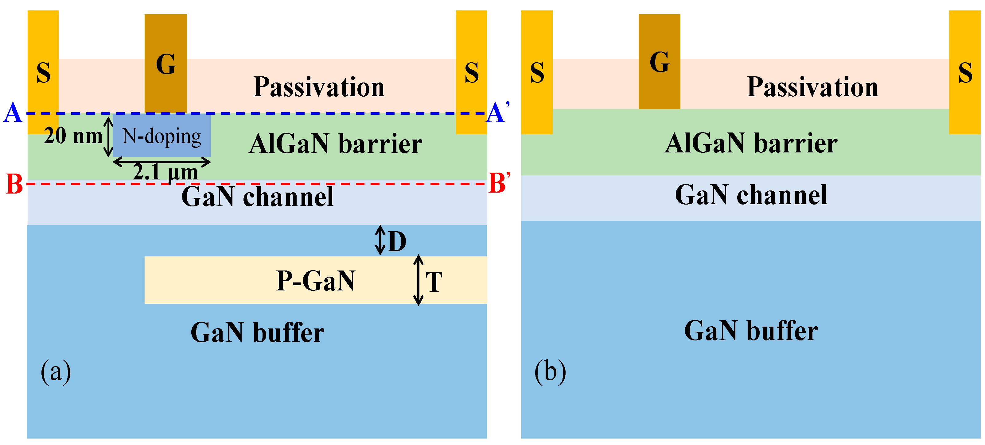
2. Device Structure and Simulation Details
3. Results and Discussion
3.1. Basic Characteristics
3.2. SET Effect
4. Conclusions
Author Contributions
Funding
Data Availability Statement
Conflicts of Interest
References
- Tian, K.; Zhao, P.; Du, J.; Yu, Q. Design optimization of wide-gate swing E-mode GaN HEMTs with junction barrier Schottky gate. J. Phys. D Appl. Phys. 2024, 57, 415107. [Google Scholar] [CrossRef]
- Liu, H.X.; Huang, H.M.; Wang, K.; Xie, Z.J.; Wang, H. Impact of composition and thickness of step-graded AlGaN barrier in AlGaN/GaN heterostructures. Mater. Sci. Semicond. Process. 2024, 178, 108460. [Google Scholar] [CrossRef]
- Cheng, J.J.; Wang, Q.Y.; Liu, Y.K.; Ding, G.; Zhang, M.M.; Yi, B.; Huang, H.M.; Yang, H.Q. Study on a p-GaN HEMT with composite passivation and composite barrier layers. Semicond. Sci. Technol. 2024, 39, 085004. [Google Scholar] [CrossRef]
- Liu, A.-C.; Huang, Y.-W.; Chen, H.-C.; Kuo, H.-C. Improvement Performance of p-GaN Gate High Electron-Mobility Transistors with GaN/AlN/AlGaN Barrier Structure. Micromachines 2024, 15, 517. [Google Scholar] [CrossRef] [PubMed]
- Husna Hamza, K.; Nirmal, D.; Augustine Fletcher, A.S.; Ajayan, J.; Natarajan, R. Enhanced drain current and cut off frequency in AlGaN/GaN HEMT with BGaN back barrier. Mater. Sci. Eng. B 2022, 284, 115863. [Google Scholar] [CrossRef]
- He, Y.W.; Zhang, L.; Cheng, Z.; Li, C.C.; He, J.H.; Xie, S.J.; Wu, X.K.; Wu, C.; Zhang, Y. Scaled InAlN/GaN HEMT on Sapphire With fT/fmax of 190/301 GHz. IEEE Trans. Electron. Device 2023, 70, 3001–3004. [Google Scholar] [CrossRef]
- Lv, R.P.; Sun, H.Q.; Yang, L.F.; Liu, Z.; Zhang, Y.H.; Li, Y.; Huang, Y.; Guo, Z.Y. Improving RF characteristic and suppress gate leakage in normally-off GaN-HEMTs using negative polarization effect and floating gate for millimeter-wave systems. Results Phys. 2024, 59, 107526. [Google Scholar] [CrossRef]
- Mounika, B.; Ajayan, J.; Bhattacharya, S.; Nirmal, D. Recent developments in materials, architectures and processing of AlGaN/GaN HEMTs for future RF and power electronic applications: A critical review. Micro Nanostruct. 2022, 168, 207317. [Google Scholar] [CrossRef]
- Zerarka, M.; Austin, P.; Bensoussan, A.; Morancho, F.; Durier, A. TCAD Simulation of the Single Event Effects in Normally-OFF GaN Transistors After Heavy Ion Radiation. IEEE Trans. Nucl. Sci. 2017, 64, 2242–2249. [Google Scholar] [CrossRef]
- Mounika, B.; Ajayan, J.; Bhattacharya, S. An intensive study on effects of lateral scaling and gate metals on the RF/DC performance of recessed T-gated Fe-doped AlN/GaN/SiC HEMTs for future RF and microwave power applications. Microelectron. Eng. 2023, 271–272, 111948. [Google Scholar] [CrossRef]
- Nelson, T.; Georgiev, D.G.; Hontz, M.R.; Khanna, R.; Ildefonso, A.; Koehler, A.D.; Hobart, A.; Khachatrian, A.; McMorrow, D. Examination of Trapping Effects on Single-Event Transients in GaN HEMTs. IEEE Trans. Nucl. Sci. 2023, 70, 328–335. [Google Scholar] [CrossRef]
- Li, K.; Hao, J.H.; Zhao, Q.; Zhang, F.; Dong, Z.W. Simulation of heavy ion irradiation effect on 3D MOSFET. AIP Adv. 2023, 13, 025143. [Google Scholar] [CrossRef]
- Liu, B.J.; Li, C.; Chen, M.H. Investigation of Single Event Transient Induced by Process Variability in 14 nm High-k/Metal Gate SOI FinFET Devices. Silicon 2023, 15, 1317–1324. [Google Scholar] [CrossRef]
- Wu, W.R.; Xu, W.T.; Qu, K.; Yang, G.G.; Yu, Z.X.; Sun, W.F. Comprehensive investigation on different ions of geostationary orbitinduced single event burnout in GaN HEMT power devices. Microelectron. Reliab. 2023, 149, 115187. [Google Scholar] [CrossRef]
- Zhang, X.; Cao, Y.; Chen, C.; Wu, L.; Wang, Z.; Su, S.; Zhang, W.; Lv, L.; Zheng, X.; Tian, W.; et al. Study on Single Event Effects of Enhanced GaN HEMT Devices under Various Conditions. Micromachines 2024, 15, 950. [Google Scholar] [CrossRef]
- Liang, Y.; Chen, R.; Han, J.; Wang, X.; Chen, Q.; Yang, H. The Study of the Single Event Effect in AlGaN/GaN HEMT Based on a Cascode Structure. Electronics 2021, 10, 440. [Google Scholar] [CrossRef]
- Das, S.; Kumari, V.; Sehra, K.; Gupta, M.; Saxena, M. TCAD Based Investigation of Single Event Transient Effect in Double ChannelAlGaN/GaN HEMT. IEEE Trans. Device Mater. Reliab. 2021, 21, 416–423. [Google Scholar] [CrossRef]
- Zhen, Z.X.; Feng, C.; Wang, Q.; Niu, D.; Wang, X.L.; Tan, M.Q. Single Event Burnout Hardening of Enhancement Mode HEMTs With Double Field Plates. IEEE Trans. Nucl. Sci. 2021, 68, 2358–2366. [Google Scholar] [CrossRef]
- Khachatrian, A.; Buchner, S.; Koehler, A.; Affouda, C.; McMorrow, D.; LaLumondiere, S.D.; Dillingham, E.C.; Bonsall, J.P.; Scofield, A.C.; Brewe, D.L. The Effect of the Gate-Connected Field Plate on Single-Event Transients in AlGaN/GaN Schottky-Gate HEMTs. IEEE Trans. Nucl. Sci. 2019, 66, 1682–1687. [Google Scholar] [CrossRef]
- Zhang, N.Q.; Keller, S.; Parish, G.; Heikman, S.; DenBaars, S.P.; Mishra, U.K. High breakdown GaN HEMT with overlapping gate structure. IEEE Electron. Device Lett. 2000, 21, 421–423. [Google Scholar] [CrossRef]
- Saito, W.; Nitta, T.; Kakiuchi, Y.; Saito, Y.; Tsuda, K.; Omura, I.; Yamaguchi, M. Suppression of dynamic on-resistance increase and gate charge measurements in high-voltage GaN-HEMTs with optimized field-plate structure. IEEE Trans. Electron. Device 2007, 54, 1825–1830. [Google Scholar] [CrossRef]
- Medjdoub, F.; Derluyn, J.; Cheng, K.; Leys, M.; Degroote, S.; Marcon, D.; Visalli, D.; Van Hove, M.; Germain, M.; Borghs, G. Low on-resistance high-breakdown normally off AlN/GaN/AlGaN DHFET on Si substrate. IEEE Electron. Device Lett. 2010, 31, 111–113. [Google Scholar] [CrossRef]
- Luo, X.; Wang, Y.; Hao, Y.; Cao, F.; Yu, C.H.; Fei, X.X. TCAD Simulation of Breakdown-Enhanced AlGaN-/GaN-Based MISFET with Electrode-Connected p-i-n Diode in Buffer Layer. IEEE Trans. Electron. Device 2018, 65, 476–482. [Google Scholar] [CrossRef]
- Du, J.F.; Liu, D.; Zhao, Z.Q.; Bai, Z.Y.; Li, L.; Mo, J.H.; Yu, Q. Design of high breakdown voltage GaN vertical HFETs with p-GaN buried buffer layers for power switching applications. Superlattices Microstruct. 2015, 83, 251–260. [Google Scholar] [CrossRef]
- Fei, X.; Wang, Y.; Luo, X.; Bao, M.; Yu, C. TCAD simulation of abreakdown-enhanced double channel GaN metal-insulator-semiconductorfield-effect transistor with a P-buried layer. Semicond. Sci. Technol. 2020, 35, 065012. [Google Scholar]
- Wang, Y.; Bao, M.; Cao, F.; Tang, J.; Luo, X. Technology Computer Aided Design Study of GaN MISFET with Double P-Buried Layers. IEEE Access 2019, 7, 87574–87581. [Google Scholar] [CrossRef]
- Fei, X.; Wang, Y.; Sun, B.; Xing, J.; Wei, W.; Li, C. Simulation study of single-event burnout in hardened GaN MISFET. Radiat. Phys. Chem. 2023, 213, 111244. [Google Scholar] [CrossRef]
- Sabui, G.; Parbrook, P.J.; Arredondo-Arechavala, M.; Shen, Z.J. Modeling and simulation of bulk gallium nitride power semiconductor devices. Aip Adv. 2016, 6, 055006. [Google Scholar] [CrossRef]
- Jia, Y.; Wang, Q.; Chen, C.; Feng, C.; Li, W.; Jiang, L.; Xiao, H.; Wang, Q.; Xu, X.; Wang, X. Simulation of a Parallel Dual-Metal-Gate Structure for AlGaN/GaN High-Electron-Mobility Transistor High Linearity Applications. Phys. Status Solidi A 2021, 218, 2100151. [Google Scholar] [CrossRef]
- Yu, C.H.; Guo, H.M.; Liu, Y.; Wu, X.D.; Zhang, L.D.; Tan, X.; Han, Y.C.; Ren, L. Simulation study on single-event burnout in field-plated Ga2O3 MOSFETs. Microelectron. Reliab. 2023, 149, 115227. [Google Scholar] [CrossRef]
- Wang, K.; Wang, Z.; Cao, Y.; Liu, H.; Chang, W.; Zhao, L.; Mei, B.; Lv, H.; Zeng, X.; Xue, Y. Study of the mechanism of single event burnout in lateral depletion-mode Ga2O3 MOSFET devices via TCAD simulation. J. Appl. Phys. 2024, 135, 145702. [Google Scholar] [CrossRef]
- Olson, B.D.; Ingalls, J.D.; Rice, C.H.; Hedge, C.C.; Cole, P.L.; Duncan, A.R.; Armstrong, S.E. Leakage Current Degradation of Gallium Nitride Transistors Due to Heavy Ion Tests. In Proceedings of the IEEE Radiation Effects Data Workshop (REDW), Boston, MA, USA, 3 December 2015. [Google Scholar]
- Weatherford, T.R. Radiation effects in high speed III-V integrated circuits. Int. J. High. Speed Electron. Syst. 2003, 13, 277–292. [Google Scholar] [CrossRef]
- Fu, W.; Xu, Y.; Yan, B.; Zhang, B.; Xu, R. Numerical simulation of local doped barrier layer AlGaN/GaN HEMTs. Superlattices Microstruct. 2013, 60, 443–452. [Google Scholar] [CrossRef]
- Luo, J.; Zhao, S.; Lin, Z.; Zhang, J.; Ma, X.; Hao, Y. Enhancement of Breakdown Voltage in AlGaN/GaN High Electron Mobility Transistors Using Double Buried p-Type Layers. Chin. Phys. Lett. 2016, 33, 067301. [Google Scholar] [CrossRef]
- Luo, X.; Wang, Y.; Cao, F.; Yu, C.; Fei, X. A breakdown enhanced AlGaN/GaN MISFET with source connected P-buried layer. Superlattices Microstruct. 2017, 112, 517–527. [Google Scholar] [CrossRef]
- Kodama, M.; Sugimoto, M.; Hayashi, E.; Soejim, N.; Ishiguro, O.; Kanechika, M.; Itoh, K.; Ueda, H.; Uesugi, T.; Kachi, T. GaN-Based Trench Gate Metal Oxide Semiconductor Field-Effect Transistor Fabricated with Novel Wet Etching. Appl. Phys. Express 2008, 1, 021104. [Google Scholar] [CrossRef]
- Arifin, P.; Sutanto, H.; Sugianto; Subagio, A. Plasma Assisted MOCVD Growth of Non-Polar GaN and AlGaN on Si(111) Substrates Utilizing GaN-AlN Buffer Layer. Coatings 2022, 12, 94. [Google Scholar] [CrossRef]


| Parameter | Value |
|---|---|
| Al0.3Ga0.7N barrier layer thickness | 25 nm |
| GaN channel layer thickness | 100 nm |
| Thickness of P-GaN buried layer (T) | 100 nm |
| Distance from channel for P-GaN buried layer (D) | 50 nm |
| P-GaN layer doping concentration (NP) | 7 × 1017 cm−3 |
| GaN buffer layer thickness | 1.4 µm |
| Gate–source spacing | 1.4 µm |
| Gate–drain spacing | 2.4 µm |
Disclaimer/Publisher’s Note: The statements, opinions and data contained in all publications are solely those of the individual author(s) and contributor(s) and not of MDPI and/or the editor(s). MDPI and/or the editor(s) disclaim responsibility for any injury to people or property resulting from any ideas, methods, instructions or products referred to in the content. |
© 2024 by the authors. Licensee MDPI, Basel, Switzerland. This article is an open access article distributed under the terms and conditions of the Creative Commons Attribution (CC BY) license (https://creativecommons.org/licenses/by/4.0/).
Share and Cite
Xiong, J.; Xie, X.; Wei, J.; Sun, S.; Luo, X. Improvement of Single Event Transient Effects for a Novel AlGaN/GaN High Electron-Mobility Transistor with a P-GaN Buried Layer and a Locally Doped Barrier Layer. Micromachines 2024, 15, 1158. https://doi.org/10.3390/mi15091158
Xiong J, Xie X, Wei J, Sun S, Luo X. Improvement of Single Event Transient Effects for a Novel AlGaN/GaN High Electron-Mobility Transistor with a P-GaN Buried Layer and a Locally Doped Barrier Layer. Micromachines. 2024; 15(9):1158. https://doi.org/10.3390/mi15091158
Chicago/Turabian StyleXiong, Juan, Xintong Xie, Jie Wei, Shuxiang Sun, and Xiaorong Luo. 2024. "Improvement of Single Event Transient Effects for a Novel AlGaN/GaN High Electron-Mobility Transistor with a P-GaN Buried Layer and a Locally Doped Barrier Layer" Micromachines 15, no. 9: 1158. https://doi.org/10.3390/mi15091158
APA StyleXiong, J., Xie, X., Wei, J., Sun, S., & Luo, X. (2024). Improvement of Single Event Transient Effects for a Novel AlGaN/GaN High Electron-Mobility Transistor with a P-GaN Buried Layer and a Locally Doped Barrier Layer. Micromachines, 15(9), 1158. https://doi.org/10.3390/mi15091158