
Cavity-BOX SOI: Advanced Silicon Substrate with Pre-Patterned BOX for Monolithic MEMS Fabrication

 ,
, 
Abstract
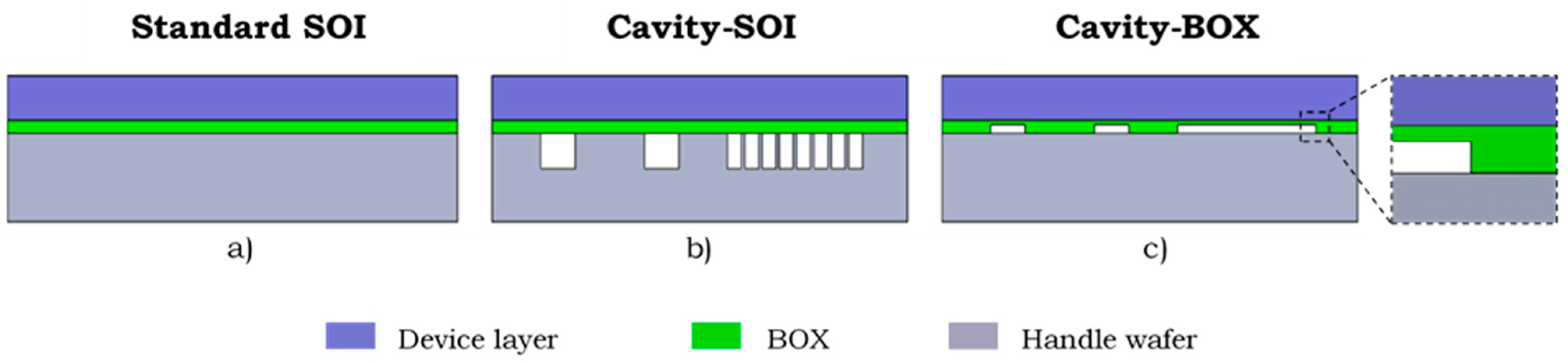
1. Introduction
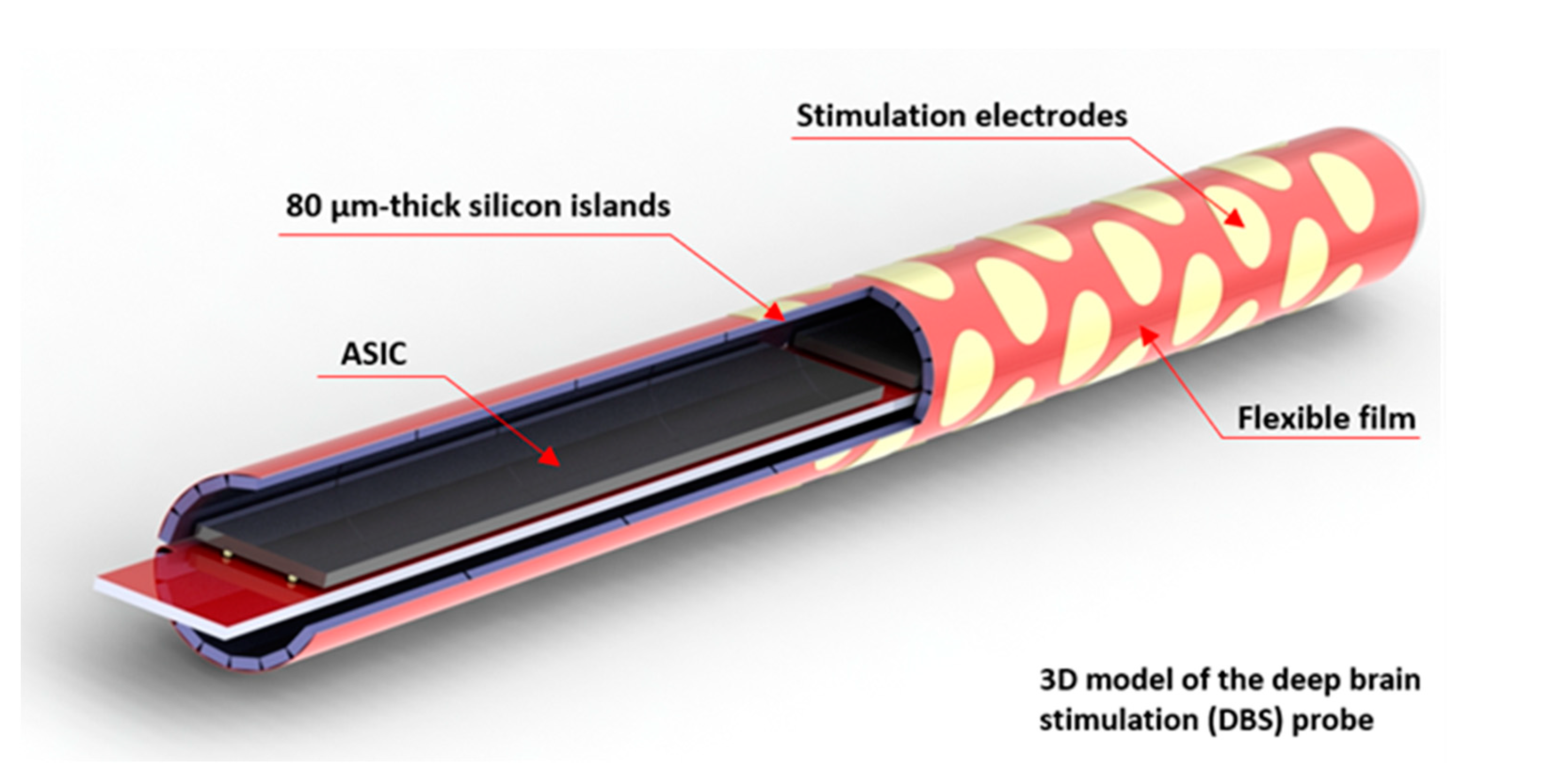
2. Deep Brain Stimulation (DBS) Probe-Process and Design
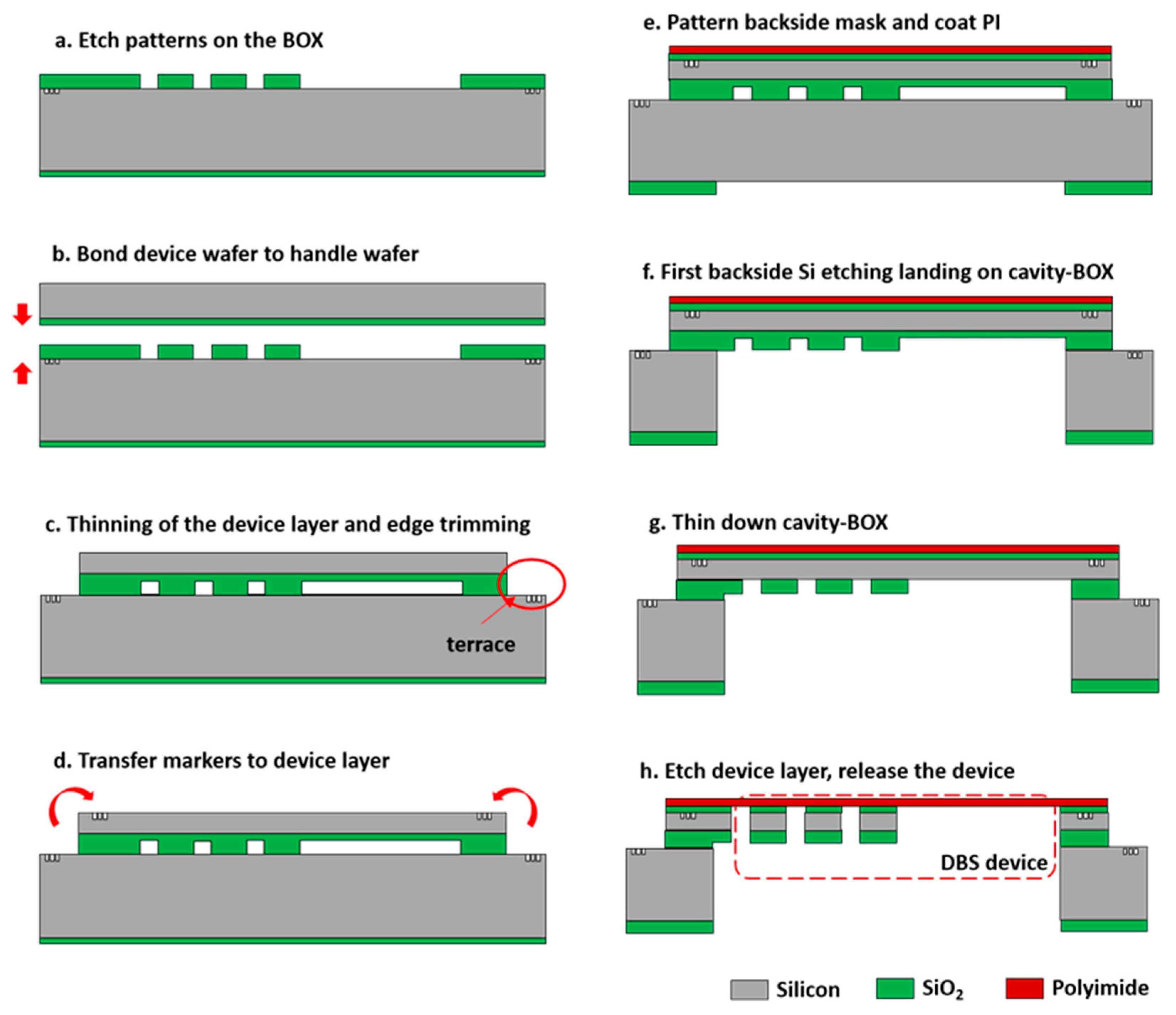
3. Fabrication
3.1. Cavity-BOX Preparation
3.2. DBS Demonstrator Fabrication
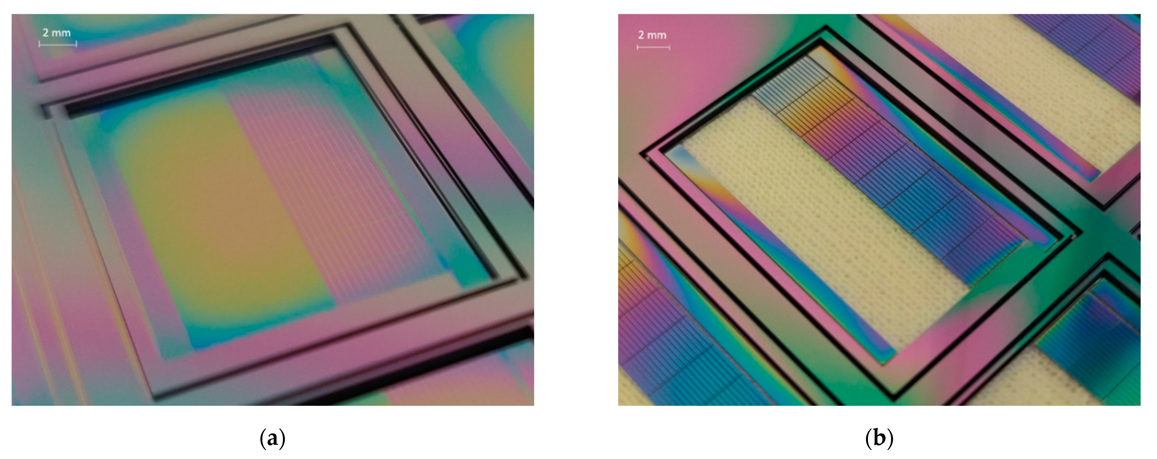
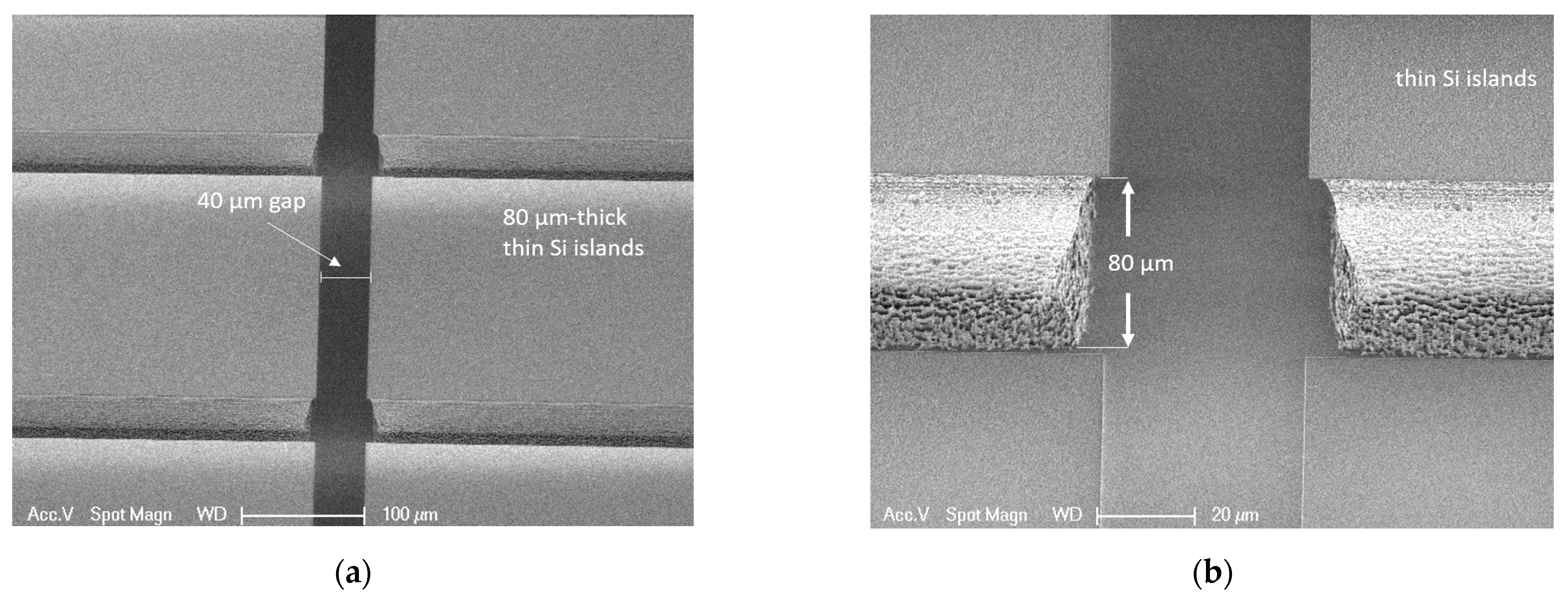
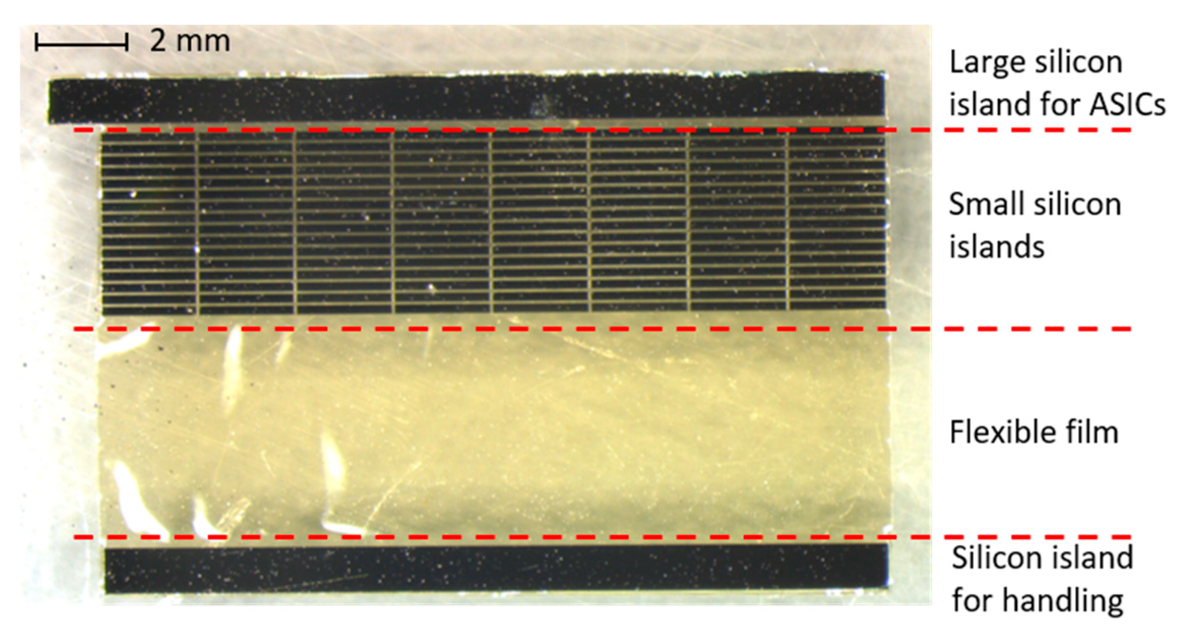
4. Results and Discussion
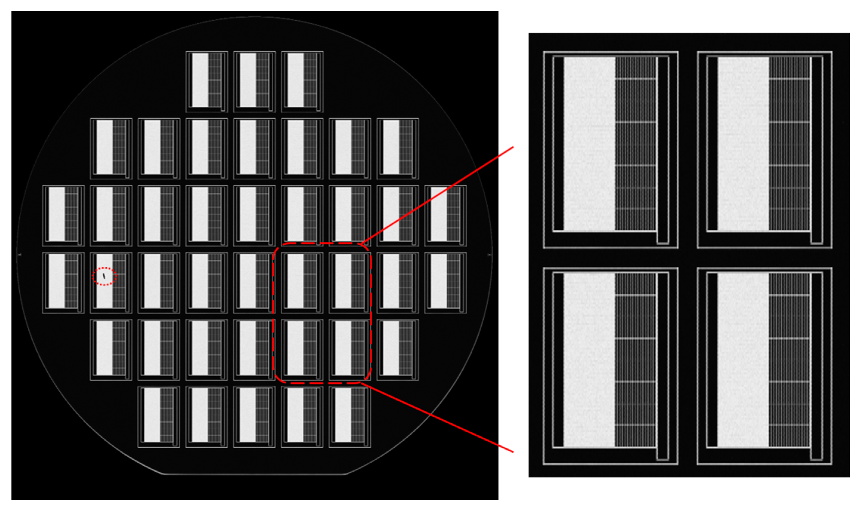
4.1. Preparation of the Cavity-BOX
4.2. Terrace Width
4.3. Backside Etching of the Demonstrator
4.4. Demonstrator Assembly
5. Conclusions
Author Contributions
Funding
Acknowledgments
Conflicts of Interest
References
- San, H.; Zhang, H.; Zhang, Q.; Yu, Y.; Cheng, X. Silicon-glass-based single piezoresistive pressure sensor for harsh environment applications. J. Micromach. Microeng. 2013, 23, 075020. [Google Scholar] [CrossRef]
- Zhang, Y.; Yang, C.; Meng, F.; Liu, G.; Gao, C.; Hao, Y. A monolithic integration multifunctional MEMS sensor based on cavity SOI wafer. In Proceedings of the SENSORS, 2014 IEEE, Valencia, Spain, 2–5 November 2014; pp. 1952–1955. [Google Scholar]
- Stoute, R.; Muganda, J.M.; Dahar, S.; Arslan, A.; Henderikx, R.J.M.; van Stiphout, P.C.M.; den Toonder, J.M.J.; Dekker, R. CMOS Compatible Embedded Microchannels. In Proceedings of the 20th International Conference on Miniaturized Systems for Chemistry and Life Sciences, Dublin, Ireland, 9–13 October 2016. [Google Scholar]
- Li, J.; Naaborg, J.; Louwerse, M.; Henneken, V.; Eugeni, C.; Dekker, R. Embedded High-Density Trench Capacitors for Smart Catheters. In Proceedings of the 2020 IEEE 8th Electronics System-Integration Technology Conference, ESTC 2020, Online, 15–18 September 2020; pp. 1–5. [Google Scholar]
- Kluba, M.; Morana, B.; Savov, A.; van Zeijl, H.; Pandraud, G.; Dekker, R. Wafer-Scale Integration for Semi-Flexible Neural Implant Miniaturization. Proceedings 2018, 2, 941. [Google Scholar] [CrossRef]
- Okmetic. SOI WAFERS. Available online: https://www.okmetic.com/products/product-portfolio/soi-wafers (accessed on 20 December 2018).
- Liu, C.; Froemel, J.; Chen, J.; Tsukamoto, T.; Tanaka, S. Laterally vibrating MEMS resonant vacuum sensor based on cavity-SOI process for evaluation of wide range of sealed cavity pressure. Microsyst. Technol. 2018. [Google Scholar] [CrossRef]
- Wu, G.; Xu, D.; Xiong, B.; Wang, Y. A high-performance bulk mode single crystal silicon microresonator based on a cavity-SOI wafer. J. Micromech. Microeng. 2012, 22, 25020. [Google Scholar] [CrossRef]
- Xu, J.; Zhang, X.; Fernando, S.N.; Chai, K.T.; Gu, Y. AlN-on-SOI platform-based micro-machined hydrophone. Appl. Phys. Lett. 2016, 109, 32902. [Google Scholar] [CrossRef]
- Luoto, H.; Henttinen, K.; Suni, T.; Dekker, J.; Mäkinen, J.; Torkkeli, A. MEMS on cavity-SOI wafers. Solid State Electron. 2007, 51, 328–332. [Google Scholar] [CrossRef]
- Mountain, C.; Kluba, M.; Bergers, L.; Snijder, J.; Dekker, R. Novel method of alignment to buried cavities in cavity-SOI wafers for advanced MEMS devices. Micro Nano Eng. 2019, 5, 100043. [Google Scholar] [CrossRef]
- Shen, W.-W.; Chen, K.-N. Three-Dimensional Integrated Circuit (3D IC) Key Technology: Through-Silicon Via (TSV). Nanoscale Res. Lett. 2017, 12. [Google Scholar] [CrossRef] [PubMed]
- Kluba, M.; Arslan, A.; Stoute, R.; Muganda, J.; Dekker, R. Single-Step CMOS Compatible Fabrication of High Aspect Ratio Microchannels Embedded in Silicon. Proceedings 2017, 1, 291. [Google Scholar] [CrossRef]


Publisher’s Note: MDPI stays neutral with regard to jurisdictional claims in published maps and institutional affiliations. |
© 2021 by the authors. Licensee MDPI, Basel, Switzerland. This article is an open access article distributed under the terms and conditions of the Creative Commons Attribution (CC BY) license (https://creativecommons.org/licenses/by/4.0/).
Share and Cite
Kluba, M.M.; Li, J.; Parkkinen, K.; Louwerse, M.; Snijder, J.; Dekker, R. Cavity-BOX SOI: Advanced Silicon Substrate with Pre-Patterned BOX for Monolithic MEMS Fabrication. Micromachines 2021, 12, 414. https://doi.org/10.3390/mi12040414
Kluba MM, Li J, Parkkinen K, Louwerse M, Snijder J, Dekker R. Cavity-BOX SOI: Advanced Silicon Substrate with Pre-Patterned BOX for Monolithic MEMS Fabrication. Micromachines. 2021; 12(4):414. https://doi.org/10.3390/mi12040414
Chicago/Turabian StyleKluba, Marta Maria, Jian Li, Katja Parkkinen, Marcus Louwerse, Jaap Snijder, and Ronald Dekker. 2021. "Cavity-BOX SOI: Advanced Silicon Substrate with Pre-Patterned BOX for Monolithic MEMS Fabrication" Micromachines 12, no. 4: 414. https://doi.org/10.3390/mi12040414
APA StyleKluba, M. M., Li, J., Parkkinen, K., Louwerse, M., Snijder, J., & Dekker, R. (2021). Cavity-BOX SOI: Advanced Silicon Substrate with Pre-Patterned BOX for Monolithic MEMS Fabrication. Micromachines, 12(4), 414. https://doi.org/10.3390/mi12040414