150–200 V Split-Gate Trench Power MOSFETs with Multiple Epitaxial Layers

 ,
, 
Abstract
1. Introduction
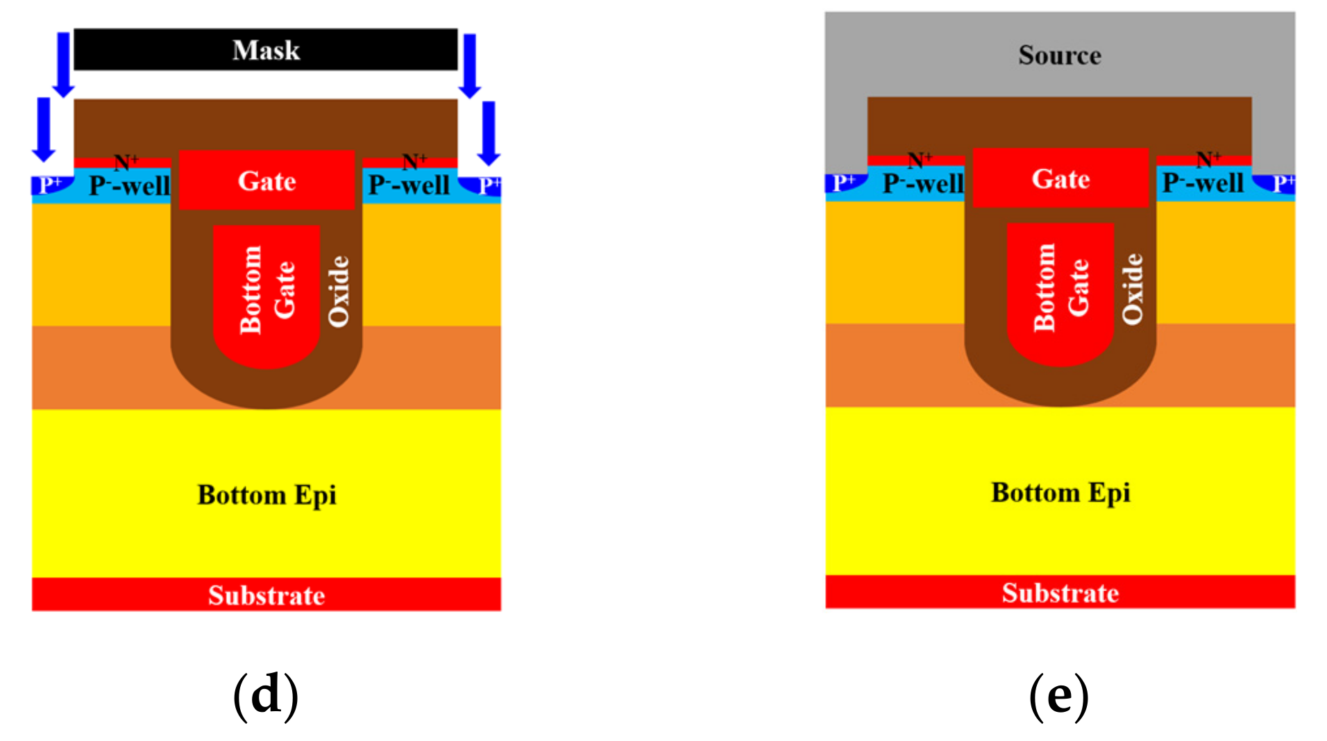
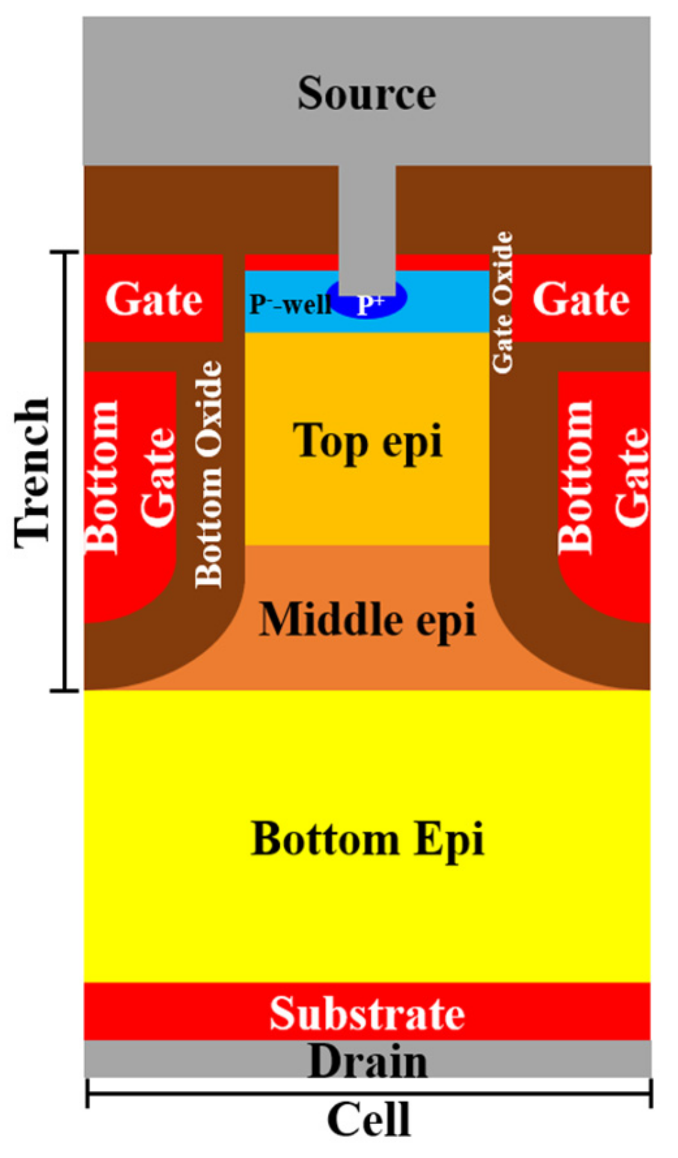
2. Device Structure and Simulation
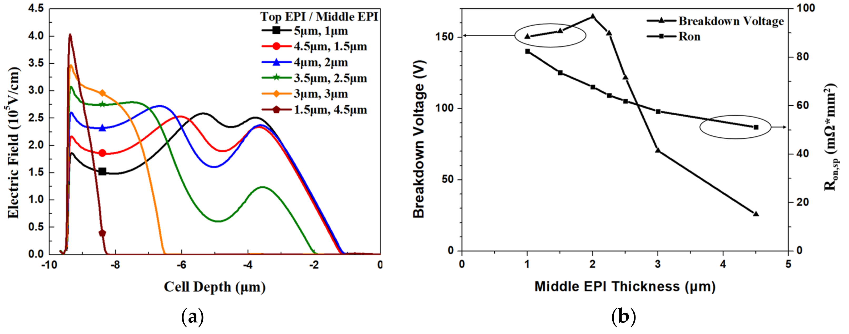
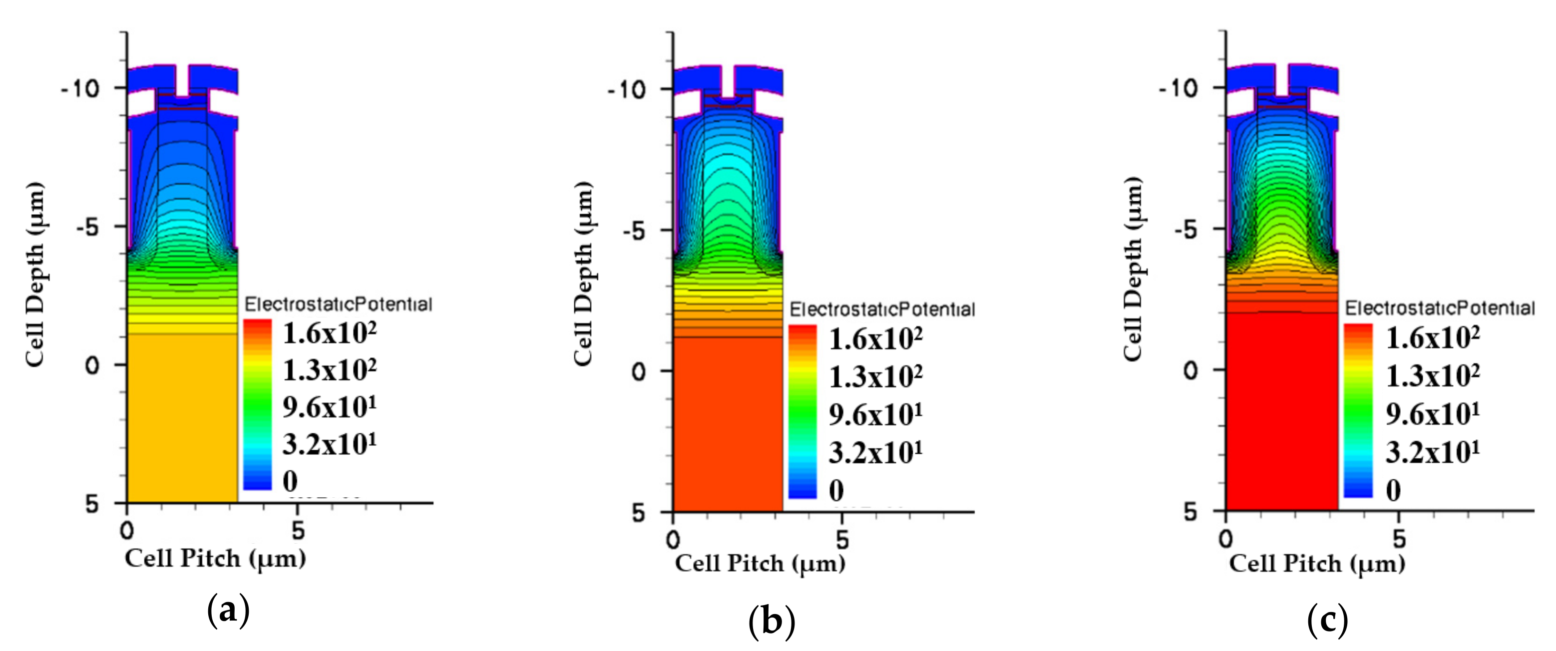
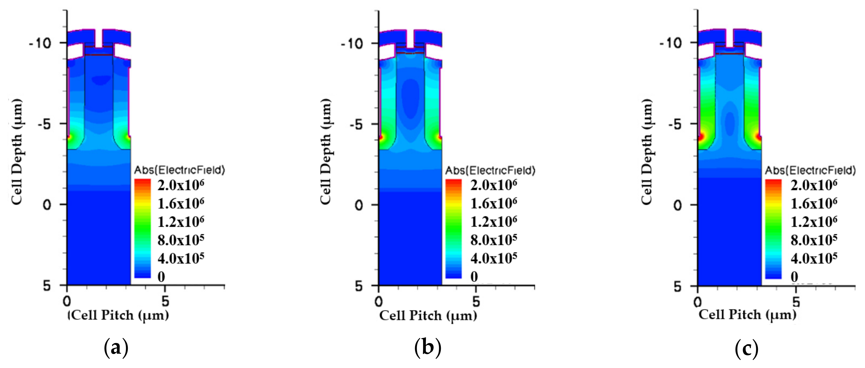
3. Results and Discussion
4. Conclusions
Author Contributions
Funding
Conflicts of Interest
References
- Takaya, H.; Morimoto, J.; Hamada, K.; Yamamoto, T.; Sakakibara, J.; Watanabe, Y.; Soejima, N. A 4H-SiC trench MOSFET with thick bottom oxide for improving characteristics. In Proceedings of the 25th International Symposium on Power Semiconductor Devices & ICs, Kanazawa, Japan, 26–30 May 2013; pp. 43–46. [Google Scholar]
- Darwish, M.; Yue, C.; Lui, K.H.; Giles, F.; Chan, B.; Chen, K.i.; Pattanayak, D.; Chen, Q.; Terrill, K.; Owyang, K. A new power W-gated trench MOSFET (WMOSFET) with high switching performance. In Proceedings of the 15th International Symposium on Power Semiconductor Devices & ICs, Cambridge, UK, 14–17 April 2003; pp. 24–27. [Google Scholar]
- Gajda, M.A.; Hodgkiss, S.W.; Mounfield, L.A.; Irwin, N.T.; Koops, G.E.J.; Dalen, R.V. Industrialisation of resurf stepped oxide technology for power transistors. In Proceedings of the 18th International Symposium on Power Semiconductor Devices & ICs, Naples, Italy, 4–8 June 2006; pp. 109–112. [Google Scholar]
- Koops, G.E.J.; Hijzen, E.A.; Hueting, R.J.E.; Zandt, M.A.A. RESURF stepped oxide (RSO) MOSFET for 85V having a record-low specific on-resistance. In Proceedings of the 16th International Symposium on Power Semiconductor Devices & ICs, Kitakyushu, Japan, 24–27 May 2004; pp. 185–188. [Google Scholar]
- Goarin, P.; Koops, G.E.J.; Van Dalen, R.; Cam, C.L.; Saby, J. Split-gate resurf Oxide (RSO) MOSFETs for 25V applications with record low gate-to-drain charge. In Proceedings of the 19th International Symposium on Power Semiconductor Devices & ICs, Jeju, Korea, 27–30 May 2007; pp. 61–64. [Google Scholar]
- Vershinin, K.; Moens, P.; Bauwens, F.; Narayanan, E.M.S.; Tack, M. A new method to improve tradeoff performance for advanced power MOSFETs. IEEE Electron. Device Lett. 2009, 30, 416–418. [Google Scholar] [CrossRef]
- Baliga, B.J. Power Semiconductor Devices having Improved High Frequency Switching and Breakdown Characteristics. U.S. Patent 5998833, 7 December 1999. [Google Scholar]
- Zeng, J. Ultra Dense Trench-Gated Power Device with the Reduced Drain-Source Feedback Capacitance and Miller Charge. U.S. Patent 6 683 346, 27 January 2004. [Google Scholar]
- Zhang, W.; Ye, L.; Fang, D.; Qizo, M.; Xizo, K.; He, B.; Li, Z.; Zhang, B. Model and experiments of small-size vertical devices with field plate. IEEE Trans. Electron. Devices 2019, 66, 1416–1421. [Google Scholar] [CrossRef]
- Williams, R.K.; Darwish, M.N.; Blanchard, R.A.; Siemieniec, R.; Rutter, P.; Kawaguchi, Y. The trench power MOSFET: Part I—history, technology, and prospects. IEEE Trans. Electron. Devices 2017, 64, 674–691. [Google Scholar] [CrossRef]
- Kobayashi, K.; Sudo, M.; Omura, I. Power loss analysis of 60 V trench field-plate MOSFETs utilizing structure based capacitance model for automotive application. In Proceedings of the 10th International Conference on Integrated Power Electronics Systems, Stuttgart, Germany, 20–22 March 2018; pp. 122–127. [Google Scholar]
- Kobayashi, K.; Sudo, M.; Omura, I. Structure-based capacitance modeling and power loss analysis for the latest high-performance slant field-plate trench MOSFET. Jpn. J. Appl. Phys. 2018, 57(4S), 04FR14. [Google Scholar] [CrossRef]
- Peake, S.T.; Rutter, P.; Hodgskiss, S.; Gajda, M.; Irwin, N. A fully realized ‘field balanced’ trenchMOS technology. In Proceedings of the 20th International Symposium on Power Semiconductor Devices & ICs, Orlando, FL, USA, 18–22 May 2008; pp. 28–31. [Google Scholar]
- Williams, R.K.; Darwish, M.N.; Blanchard, R.A.; Siemieniec, R.; Rutter, P.; Kawaguchi, Y. The trench power MOSFET—Part II: Application specific VDMOS, LDMOS, packaging, and reliability. IEEE Trans. Electron. Devices 2017, 64, 692–712. [Google Scholar] [CrossRef]
- Wang, Y.; Hu, H.F.; Dou, Z.; Yu, C.H. Way of operation to improve performance for advanced split-gate resurf stepped oxide UMOSFET. IET Power Electron. 2014, 7, 2964–2968. [Google Scholar] [CrossRef]
- Park, C.; Havanur, S.; Shibib, A.; Terrill, K. 60 V rating split gate trench MOSFETs having best-in-class specific resistance and figure-of-merit. In Proceedings of the 28th International Symposium on Power Semiconductor Devices & ICs, Prague, Czech Republic, 12–16 June 2016; pp. 387–390. [Google Scholar]
- Takaya, H.; Miyagi, K.; Hamada, K.; Okura, Y.; Tokura, N.; Kuroyanagi, A. Floating island and thick bottom oxide trench gate MOSFET (FITMOS)—A 60V ultra low on-resistance novel MOSFET with superior internal body diode. In Proceedings of the 17th International Symposium on Power Semiconductor Devices & ICs, Santa Barbara, CA, USA, 23–26 June 2005; pp. 1–4. [Google Scholar]
- Park, C.; Azam, M.; Dengel, G.; Shibib, A.; Terrill, K. A new 200 V dual trench MOSFET with stepped oxide for ultra low RDS(on). In Proceedings of the 31st International Symposium on Power Semiconductor Devices & ICs, Shanghai, China, 19–23 May 2019; pp. 95–98. [Google Scholar]
- Chen, Y.; Liang, Y.C.; Samudra, G.S. Design of gradient oxide-bypassed superjunction power MOSFET devices. IEEE Trans. Power Electron. 2007, 22, 1303–1310. [Google Scholar] [CrossRef]
- Kobayashi, K.; Kato, H.; Nishiguchi, T.; Shimomura, S.; Ohno, T.; Nishiwaki, T.; Aida, K.; Ichinoseki, K.; Oasa, K.; Kawaguchi, Y. 100-V class two-step-oxide field-plate trench MOSFET to achieve optimum RESURF effect and ultralow on-resistance. In Proceedings of the 31st International Symposium on Power Semiconductor Devices & ICs, Shanghai, China, 19–23 May 2019; pp. 99–102. [Google Scholar]
- Kobayashi, K.; Nishiguchi, T.; Katoh, S.; Kawano, T.; Kawaguchi, Y. 100 V class multiple stepped oxide field plate trench MOSFET (MSO-FP-MOSFET) aimed to ultimate structure realization. In Proceedings of the 27th International Symposium on Power Semiconductor Devices & ICs, Kowloon Shangri-La, Hong Kong, 10–14 May 2015; pp. 141–144. [Google Scholar]
- Daniel, B.J.; Parikh, C.D.; Patil, M.B. Modeling of the coolMOS/sup TM/ transistor—Part I: Device physics. IEEE Trans. Electron. Devices 2002, 49, 916–922. [Google Scholar] [CrossRef]
- Lorenz, L.; Deboy, G.; Knapp, A.; Marz, M. COOLMOS/sup TM/-a new milestone in high voltage power MOS. In Proceedings of the 11th International Symposium on Power Semiconductor Devices & ICs, Toronto, ON, Canada, 26–28 May 1999; pp. 3–10. [Google Scholar]
- Kondekar, P.N.; Parikh, C.D.; Patil, M.B. Analysis of breakdown voltage and on resistance of super junction power MOSFET CoolMOS/sup TM/ using theory of novel voltage sustaining layer. In Proceedings of the 33rd Annual IEEE Power Electronics Specialists Conference, Cairns, QLD, Australia, 23–27 June 2002; pp. 1769–1775. [Google Scholar]
- Tian, K.; Hallén, A.; Qi, J.; Shenhui, M.; Fei, X.; Zhang, A.; Liu, W. An improved 4H-SiC trench-gate MOSFET with low on-resistance and switching loss. IEEE Trans. Electron. Devices 2019, 66, 2307–2313. [Google Scholar] [CrossRef]
- Chen, L.; Guy, O.J.; Jennings, M.R.; Igic, P.; Wilks, S.P.; Mawby, P.A. Study of 4H–SiC trench MOSFET structures. Solid State Electron. 2005, 49, 1081–1085. [Google Scholar] [CrossRef]
- Palmour, J.W.; Cheng, L.; Pala, V.; Brunt, E.V.; Lichtenwalner, D.J.; Wang, G.; Richmond, J.; O’Loughlin, M.; Ryu, S.; Allen, S.T.; et al. Silicon carbide power MOSFETs: Breakthrough performance from 900 V up to 15 kV. In Proceedings of the 26th International Symposium on Power Semiconductor Devices & ICs, Waikoloa, HI, USA, 15–19 June 2014; pp. 79–82. [Google Scholar]
- Li, X.; Tong, X.; Huang, A.Q.; Tao, H.; Zhou, K.; Jiang, Y.F.; Jiang, J.N.; Deng, X.C.; She, X.; Zhang, B.; et al. SiC trench MOSFET with integrated self-assembled three-level protection schottky barrier diode. IEEE Trans. Electron. Devices 2018, 65, 347–351. [Google Scholar] [CrossRef]
- Wang, Q.; Li, M.; Sharp, J.; Challa, A. The effects of double-epilayer structure on threshold voltage of ultralow voltage trench power MOSFET devices. IEEE Trans. Electron. Devices 2007, 54, 833–839. [Google Scholar] [CrossRef]
- Li, M.; Crellin, A.; Ho, I.; Wang, Q. Double-epilayer structure for low drain voltage rating n-channel power trench MOSFET devices. IEEE Trans. Electron. Devices 2008, 55, 1749–1755. [Google Scholar] [CrossRef]
- ISE-TCAD Manuals; Release 10.0; Integrated Systems Engineering: Zurich, Switzerland, 2004.
- Yamaguchi, H.; Urakami, Y.; Sakakibara, J. Breakthrough of on-resistance Si limit by Super 3D MOSFET under 100V breakdown voltage. In Proceedings of the 18th International Symposium on Power Semiconductor Devices & ICs, Naples, Italy, 4–8 June 2006. [Google Scholar]
- Hattori, Y.; Nakashima, K.; Kuwahara, M.; Yoshida, T.; Yamauchi, S.; Yamaguchi, H. Design of a 200V super junction MOSFET with n-buffer regions and its fabrication by trench filling. In Proceedings of the 16th International Symposium on Power Semiconductor Devices & ICs, Kitakyushu, Japan, 24–27 May 2004; pp. 189–192. [Google Scholar]
- Weber, Y.; Morancho, F.; Reynes, J.; Stefanov, E. A New Optimized 200V Low On-Resistance Power FLYMOSFET. In Proceedings of the 20th International Symposium on Power Semiconductor Devices & ICs, Orlando, FL, USA, 18–22 May 2008; pp. 149–152. [Google Scholar]
- Miura, Y.; Ninomiya, H.; Kobayashi, K. High performance superjunction UMOSFETs with split p-columns fabricated by multi-ion-implantations. In Proceedings of the 17th International Symposium on Power Semiconductor Devices & ICs, Santa Barbara, CA, USA, 23–26 May 2005; pp. 1–4. [Google Scholar]
- Van Dalen, R.; Rochefort, C. Electrical characterisation of vertical vapor phase doped (VPD) RESURF MOSFETs. In Proceedings of the 16th International Symposium on Power Semiconductor Devices & ICs, Kitakyushu, Japan, 24–27 May 2004; pp. 451–454. [Google Scholar]
- Nitta, T.; Minato, T.; Yano, M.; Uenisi, A.; Harada, M.; Hine, S. Experimental results and simulation analysis of 250V super trench power MOSFET (STM). In Proceedings of the 12th International Symposium on Power Semiconductor Devices & ICs, Toulouse, France, 22–25 May 2000; pp. 77–80. [Google Scholar]
- Kurosaki, T.; Shishido, H.; Kitada, M.; Oshima, K.; Kunori, S.; Sugai, A. 200V multi RESURF trench MOSFET (MR-TMOS). In Proceedings of the 15th International Symposium on Power Semiconductor Devices & ICs, Cambridge, UK, 14–17 April 2003; pp. 211–214. [Google Scholar]
- Chen, X.B.; Mawby, P.A.; Board, K.; Salamab, C.A.T. Theory of a novel voltage-sustaining layer for power devices. Microelectron. J. 1998, 29, 1005–1011. [Google Scholar] [CrossRef]
- Chen, Y.; Liang, Y.C.; Samudra, G.S. Theoretical analyses of oxide-bypassed superjunction power metal oxide semiconductor field effect transistor devices. Jpn. J. Appl. Phys. 2005, 44(2R), 847. [Google Scholar] [CrossRef]


| Parameter | Value |
|---|---|
| Cell pitch | 3.24 µm |
| Thickness of top EPI | 4 µm |
| Resistance of top EPI | 0.9 Ω·cm |
| Thickness of middle EPI | 2 µm |
| Resistance of middle EPI | 0.16 Ω·cm |
| Thickness of bottom EPI | 4 µm |
| Resistance of bottom EPI | 0.68 Ω·cm |
| Depth of trench | 6 µm |
| Width of trench | 1.8 µm |
| Thickness of bottom oxide | 0.8 µm |
| Thickness of gate oxide | 0.06 µm |
| Device | EPI Thickness (µm) | EPI Resistance (Ω·cm) |
|---|---|---|
| Single EPI | 10 | 1.4 |
| Double EPIs | Top EPI = 6 | Top EPI = 0.35 |
| Bottom EPI = 4 | Bottom EPI = 1.4 | |
| Triple EPIs | Top EPI = 4 | Top EPI = 0.9 |
| Middle EPI = 2 | Middle EPI = 0.16 | |
| Bottom EPI = 4 | Bottom EPI = 0.68 |
| Device | Breakdown Voltage (V) | Ron (mΩ·mm2) | EPI Thickness (µm) |
|---|---|---|---|
| Single EPI | 130.93 | 181.16 | 10 |
| Double EPIs | 153.85 | 98.23 | 10 |
| Triple EPIs | 164.49 | 67.79 | 10 |
| Device | EPI Thickness (µm) | EPI Resistance (Ω·cm) | Trench Depth (µm) |
|---|---|---|---|
| Single EPI | 15 | 2 | 8 |
| Double EPIs | Top EPI = 9 | Top EPI = 0.35 | 8 |
| Bottom EPI = 4 | Bottom EPI = 1.4 | ||
| Triple EPIs | Top EPI = 4 | Top EPI = 0.9 | 6 |
| Middle EPI = 2 | Middle EPI = 0.16 | ||
| Bottom EPI = 4 | Bottom EPI = 0.68 |
| Device | Breakdown Voltage (V) | Ron (mΩ·mm2) | Cell Pitch (µm) |
|---|---|---|---|
| Single EPI | 164.2 | 369.85 | 3.24 |
| Double EPIs | 164.23 | 109.56 | 3.24 |
| Triple EPIs | 164.49 | 67.79 | 3.24 |
| Device | EPI Thickness (µm) | EPI Resistance (Ω·cm) | Breakdown Voltage (V) | Ron (mΩ·mm2) |
|---|---|---|---|---|
| Single EPI | 16 | 4.8 | 222.79 | 729.7 |
| Double EPIs | Top EPI = 6 | Top EPI = 0.3 | 221.73 | 286.47 |
| Bottom EPI = 9 | Bottom EPI = 3 | |||
| Triple EPIs | Top EPI = 4 | Top EPI = 0.8 | 221.33 | 184.36 |
| Middle EPI = 2 | Middle EPI = 0.17 | |||
| Bottom EPI = 7.5 | Bottom EPI = 2.1 |
© 2020 by the authors. Licensee MDPI, Basel, Switzerland. This article is an open access article distributed under the terms and conditions of the Creative Commons Attribution (CC BY) license (http://creativecommons.org/licenses/by/4.0/).
Share and Cite
Chien, F.-T.; Wang, Z.-Z.; Lin, C.-L.; Kang, T.-K.; Chen, C.-W.; Chiu, H.-C. 150–200 V Split-Gate Trench Power MOSFETs with Multiple Epitaxial Layers. Micromachines 2020, 11, 504. https://doi.org/10.3390/mi11050504
Chien F-T, Wang Z-Z, Lin C-L, Kang T-K, Chen C-W, Chiu H-C. 150–200 V Split-Gate Trench Power MOSFETs with Multiple Epitaxial Layers. Micromachines. 2020; 11(5):504. https://doi.org/10.3390/mi11050504
Chicago/Turabian StyleChien, Feng-Tso, Zhi-Zhe Wang, Cheng-Li Lin, Tsung-Kuei Kang, Chii-Wen Chen, and Hsien-Chin Chiu. 2020. "150–200 V Split-Gate Trench Power MOSFETs with Multiple Epitaxial Layers" Micromachines 11, no. 5: 504. https://doi.org/10.3390/mi11050504
APA StyleChien, F.-T., Wang, Z.-Z., Lin, C.-L., Kang, T.-K., Chen, C.-W., & Chiu, H.-C. (2020). 150–200 V Split-Gate Trench Power MOSFETs with Multiple Epitaxial Layers. Micromachines, 11(5), 504. https://doi.org/10.3390/mi11050504