Article

Design and Optimization of Germanium-Based Gate-Metal-Core Vertical Nanowire Tunnel FET

1
School of Electronics Engineering, Kyungpook National University, Daegu 41566, Korea
2
Center for BioMicroSystems, Brain Science Institute, Korea Institute of Science and Technology (KIST), Seoul 02792, Korea
*
Author to whom correspondence should be addressed.
Micromachines 2019, 10(11), 749; https://doi.org/10.3390/mi10110749
Submission received: 14 October 2019 / Revised: 28 October 2019 / Accepted: 30 October 2019 / Published: 31 October 2019
(This article belongs to the Special Issue Extremely-Low-Power Devices and Their Applications)

Abstract

:
In this paper, a germanium-based gate-metal-core vertical nanowire tunnel field effect transistor (VNWTFET) has been designed and optimized using the technology computer-aided design (TCAD) simulation. In the proposed structure, by locating the gate-metal as a core of the nanowire, a more extensive band-to-band tunneling (BTBT) area can be achieved compared with the conventional core–shell VNWTFETs. The channel thickness (Tch), the gate-metal height (Hg), and the channel height (Hch) were considered as the design parameters for the optimization of device performances. The designed gate-metal-core VNWTFET exhibits outstanding performance, with an on-state current (Ion) of 80.9 μA/μm, off-state current (Ioff) of 1.09 × 10⁻¹² A/μm, threshold voltage (Vt) of 0.21 V, and subthreshold swing (SS) of 42.8 mV/dec. Therefore, the proposed device was demonstrated to be a promising logic device for low-power applications.

1. Introduction

The power consumption of future transistors has become one of the most important problems in the semiconductor industry. As the device dimensions, such as the minimum feature size, are scaled down, the importance of the off-state power as well as the active power becomes significant. Particularly, low standby power and low supply voltage (VDD) operation are necessary in various electronics applications, such as mobile devices, wearable devices, and internet-of-things (IoT) systems [1,2,3]. Considering these aspects, the tunnel field-effect transistor (TFET) is one of the most promising logic devices. TFETs have advantages such as low off-state current (Ioff), low subthreshold swing (SS), and low power consumption compared with the conventional metal-oxide-semiconductor field-effect transistors (MOSFETs). In particular, TFETs can have an SS lower than 60 mV/dec, which cannot be achieved by the conventional MOSFETs at room temperature because of their operation mechanism [4,5,6,7]. However, the conventional silicon-based TFETs exhibit several critical problems, in particular, low on-state current (Ion). Due to the large bandgap (Eg) of Si, the amount of electron band-to-band tunneling (BTBT) is insufficient, thus resulting in a small Ion [8,9,10,11]. Therefore, various studies have been conducted to improve these problems in material or structural approaches. TFETs using small Eg materials, such as Ge, at the source region exhibit an improvement in the amount of source-to-channel BTBT [12]. Furthermore, III–V heterojunction TFETs have been investigated for enhancing the electrical properties [13,14,15]. In addition to those experiments, many attempts have been performed in structural approaches to overcome the drawbacks, such as line TFET, U-gate TFET, T-shaped TFET, L-shaped TFET, and vertical nanowire TFET (VNWTFET) [15,16,17,18,19,20,21,22,23,24]. However, it is still necessary to study TFETs having superior performances and a small size.
In this work, a Ge-based gate-metal-core VNWTFET has been optimally designed and analyzed using the technology computer-aided design (TCAD) simulations. By using the gate-metal-core structure, the proposed device has a wider BTBT junction and, thus, higher current drivability can be obtained at the same size as that of the conventional VNWTFETs. Direct current (DC) characteristics such as Ion, Ioff, the on–off current ratio (Ion/Ioff), threshold voltage (Vt), and SS are investigated to evaluate the device performance. Moreover, several device parameters were modulated to obtain the optimized design values.

2. Device Structure and Description

Figure 1 shows the cross-sectional view of the proposed Ge-based gate-metal-core VNWTFET with a gate radius (Rg) of 10 nm and a gate dielectric thickness (Tox) of 2 nm. The gate dielectric material is hafnium oxide (HfO2), which enhances the current performances because of a higher gate controllability. The lower Eg and lower electron effective mass (me*) of Ge can increase the BTBT rate [12]. The work function of the gate metal is 4.27 eV. The doping concentrations of the source, channel, and drain are p-type 1 × 1020 cm−3, p-type 1 × 1016 cm−3, and n-type 5 × 1018 cm−3, respectively. Ion is defined as the drain current (IDS) at the gate voltage (VGS) = the drain voltage (VDS) = 0.55 V, for low-power applications. Further, the threshold voltage (Vt) is extracted using a constant-current method [25].
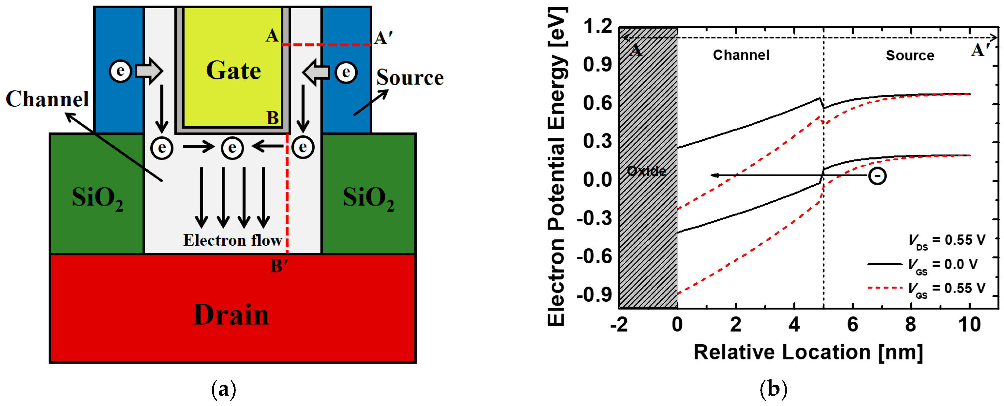
Figure 2 shows the mechanism of the current flow in the proposed device. As indicated in Figure 2a, the electrons are tunneled mainly from the source to the channel regions in the lateral path and the tunneled electrons drift toward the drain region by VDS. When the positive VGS is applied, the energy bands in the channel region are lowered and BTBT occurs at the channel–source interfaces as shown in Figure 2b. Therefore, the channel thickness (Tch) and the gate-metal height (Hg) were considered as design variables for optimization processes because Tch and Hg determine the tunneling probability and current drivability. Furthermore, the proposed gate-metal-core structure has the advantage that it proposes a wider source–channel junction area (A = 2π × (Rg + Tox + Tch) × Hg) than the conventional core–shell structure (A = 2π × Tch × Hg) in the same dimensions. Additionally, in the case of TFETs, a short source-to-drain distance causes the leakage current at the off-state and the ambipolar behavior when the negative VGS is applied. Thus, the channel height (Hch) was also considered as a design parameter. The silicon dioxide (SiO2) is placed between the source and drain regions to suppress the leakage current.
The device design and analysis are performed with the Sentaurus TCAD simulation. During the simulation process, various physical models were included for the higher accuracy. A nonlocal BTBT model was applied because the drive current of the proposed device is totally affected by the amount of tunneled electrons. The generation rate (Rnet) by the nonlocal BTBT mechanism can be obtained by the follow equation:
R net = A ( F F 0 ) P exp ( B F )
where F0 = 1 V/cm, P = 2.5 for the phonon-assisted tunneling process. At T = 300 K, the prefactor, A, and the exponential factor, B, for the phonon-assisted tunneling process can be expressed by the follow equations:
A = g ( m c m v ) 3 / 2 ( 1 + 2 N op ) D 2 op ( q F 0 ) 5 / 2 2 21 / 4 h 5 / 2 m r 5 / 4 ρ ε op E g 7 / 4
B = 2 7 / 2 π m r 1 / 2 E g 3 / 2 3 q h
where g is a degeneracy factor, h is Plank’s constant, and Dop, εop, and Nop are the deformation potential, energy, and number of optical phonons, respectively. ρ is the mass density. mC and mV are the effective mass in the conduction band and the valance band, respectively, with the relationship of 1 m r = 1 m V + 1 m C . According to the Equations (1)–(3), the proposed Ge-based TFET can achieve the higher Rnet due to the low me* and the low Eg. The Fermi–Dirac statistical model was applied because the electrons in thermal equilibrium with a semiconductor lattice obey Fermi–Dirac statistics. In addition, the Shockley–Read–Hall (SRH) recombination model, auger recombination model, and trap-assisted-tunneling (TAT) model were involved because the recombination/generation, which influences the leakage current in the device, is greatly affected by the SRH and TAT mechanism. Moreover, the bandgap narrowing model, doping dependent mobility model, and quantum confinement effect were considered to estimate the device performances more accurately [26].

3. Results and Discussion

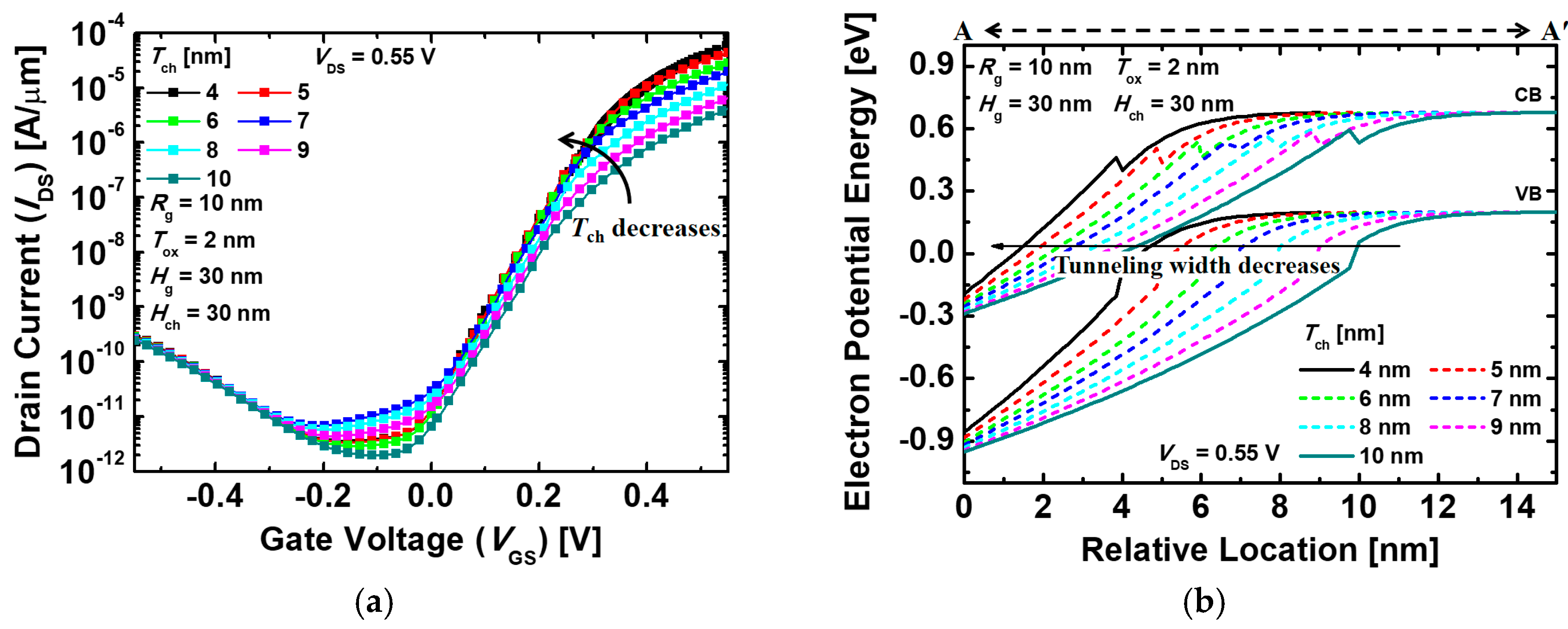
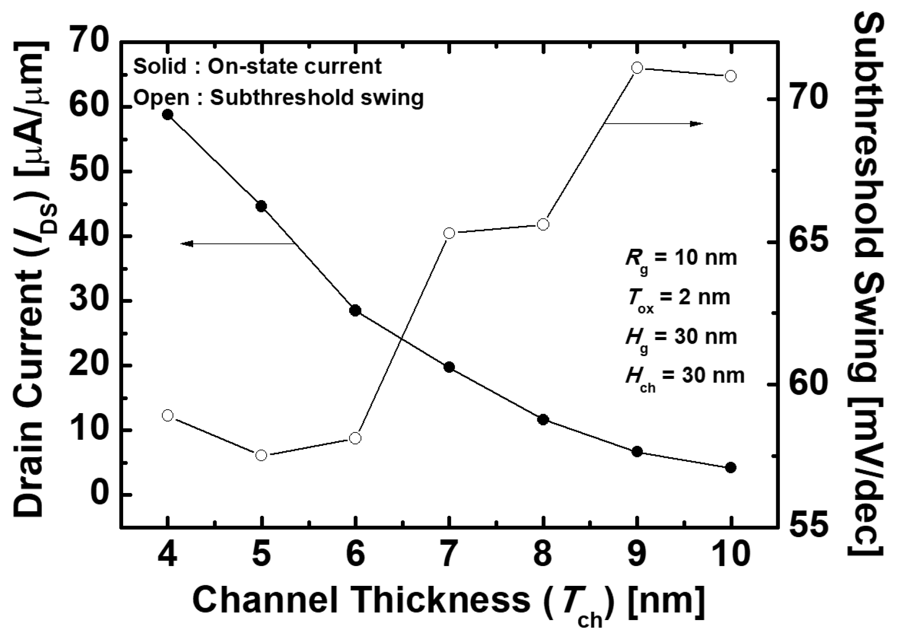
Figure 3a shows the IDSVGS transfer characteristics of the proposed gate-metal-core VNWTFETs that vary with different Tch. As Tch gets thinner, Ion increases since the effective tunneling barrier width decreases. Figure 3b depicts the energy band diagrams of the proposed devices with different Tch. The electric field across the channel region also gets stronger as Tch decreases, resulting in the enhancement of the gate controllability. Thus, the thinner Tch, having an energy band with a sharp slope, results in an increase of the electron tunneling rate. Moreover, Ioff also increases as Tch becomes thinner. When Tch is 6 nm, however, Ioff decreases because of the increment of the resistance of the channel (Rch), and then Ioff increases again as Tch further decreases. Figure 4 indicates the Ion and SS characteristics of the proposed devices with the different Tch. As described earlier, it is shown that Ion increases as Tch reduces. Unlike Ion, however, SS improved until Tch becomes 5 nm, having the minimum value of 57.5 mV/dec, and thereafter increases because of the increment of Ioff. On the other hand, the ambipolar behavior was scarcely affected by Tch, since Hch, which contributes to the leakage current when the negative VGS being applied is constant. Since SS is as crucial as Ion in the performance of the logic devices, it is desirable that Tch is adjusted to be 5 nm. Consequently, Ion = 4.46 × 10⁻⁵ A/μm, Ioff = 1.35 × 10⁻¹¹ A/μm, Vt = 0.24 V, Ion/Ioff = 3.3 × 10⁶, and SS = 57.5 mV/dec are obtained at Tch = 5 nm.
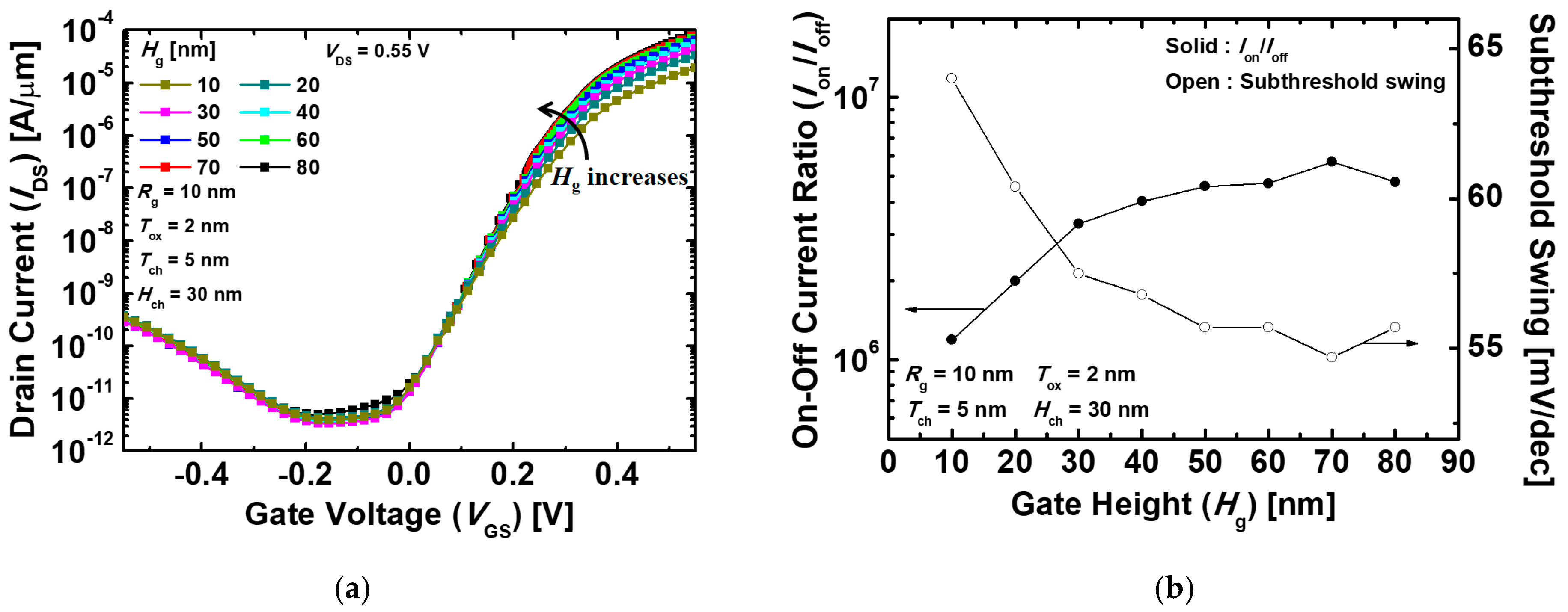
Figure 5a shows the IDSVGS transfer characteristics of the proposed devices according to variation in Hg. Each curve was extracted from the devices with the different Hg varying from 10 to 80 nm at Tch = 5 nm. The higher Hg widens the tunneling area, resulting in the enhancement of Ion because the IDS of TFETs is totally affected by the amount of the tunneled electrons. Meanwhile, Ioff also tends to increase slightly with the higher Hg for the same reason mentioned above. However, when Hg = 30 nm and Hg = 70 nm, Ioff decreased because the increment of Rch, which resulted from the longer current path, dominates over the increase of the amount of the electron tunneling at the off-state. Furthermore, the increase of Rch deteriorates the rate of the Ion increment, thus, Ion is gradually saturated. For these reasons, Ion/Ioff and SS have the largest value and the lowest value at Hg = 70 nm, respectively, as indicated in Figure 5b. Therefore, optimized values were obtained with Ion = 8.22 × 10⁻⁵ A/μm, Ioff = 1.45 × 10⁻¹¹ A/μm, Vt = 0.21 V, Ion/Ioff = 5.67 × 10⁶, and SS = 54.7 mV/dec at Tch = 5 nm and Hg = 70 nm.
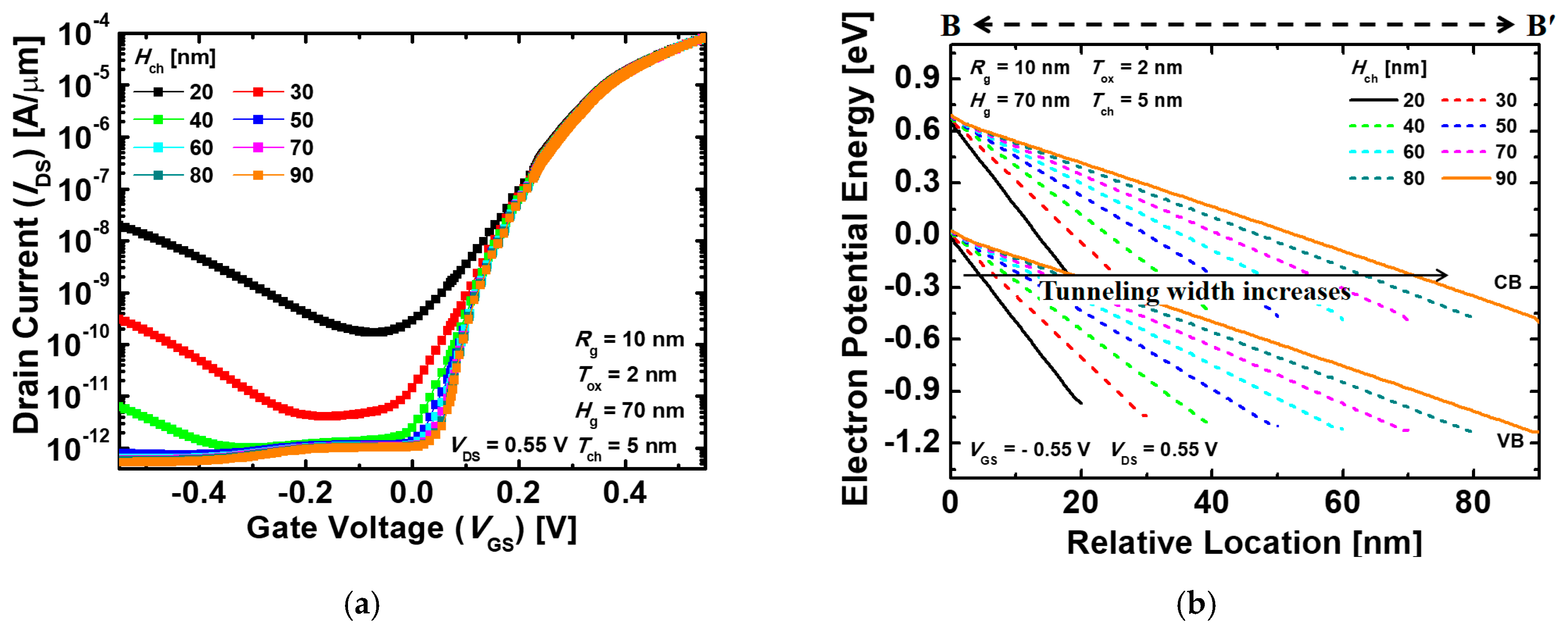
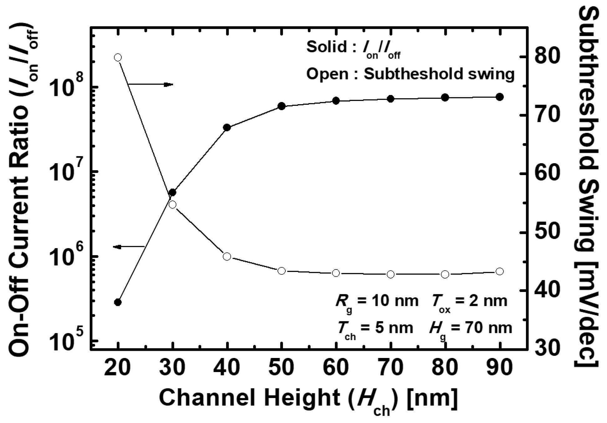
Figure 6a shows the IDSVGS transfer characteristics of the proposed devices that vary with Hch. In the proposed device, the ambipolar behavior, when the negative VGS is applied, is mainly affected by the amount of the electron tunneling from the source and channel region to the drain region. Figure 6b depicts the energy band diagrams of the proposed devices that vary with Hch at VGS = −0.55 V and VDS = 0.55 V. With the lower Hch, the energy band of the channel is lowered by VDS, as in the conventional short channel TFETs [27]. Therefore, the longer Hch where VDS has less effect on the channel has the thicker tunneling barrier width at the channel–drain junction and, thus, suppresses the electron tunneling from the channel to the drain. In addition to the foregoing, as Hch increases, Rch increases because the current path also becomes longer. As a result, Ioff decreases gradually with the Hch increasing. The increase in Rch also deteriorates Ion for the same reason. Figure 7 indicates Ion/Ioff and SS characteristics of the proposed devices with the different Hch varying from 20 to 90 nm. Ion/Ioff is gradually improved as Hch increases, and is then almost saturated when Hch = 80 nm. Moreover, SS has minimum values at Hch = 80 nm and then increases at Hch = 90 nm. As mentioned above, because of the effect of Rch, Ion and Ioff decrease constantly with increasing Hch, and the decrease in Ion dominates over Ioff when Hch = 80 nm. Finally, the optimized device is achieved with Ion = 8.09 × 10⁻⁵ A/μm, Ioff = 1.09 × 10⁻¹² A/μm, Vt = 0.21 V, Ion/Ioff = 7.45 × 10⁷, and SS = 42.8 mV/dec at Tch = 5 nm, Hg = 70 nm, and Hch = 80 nm.
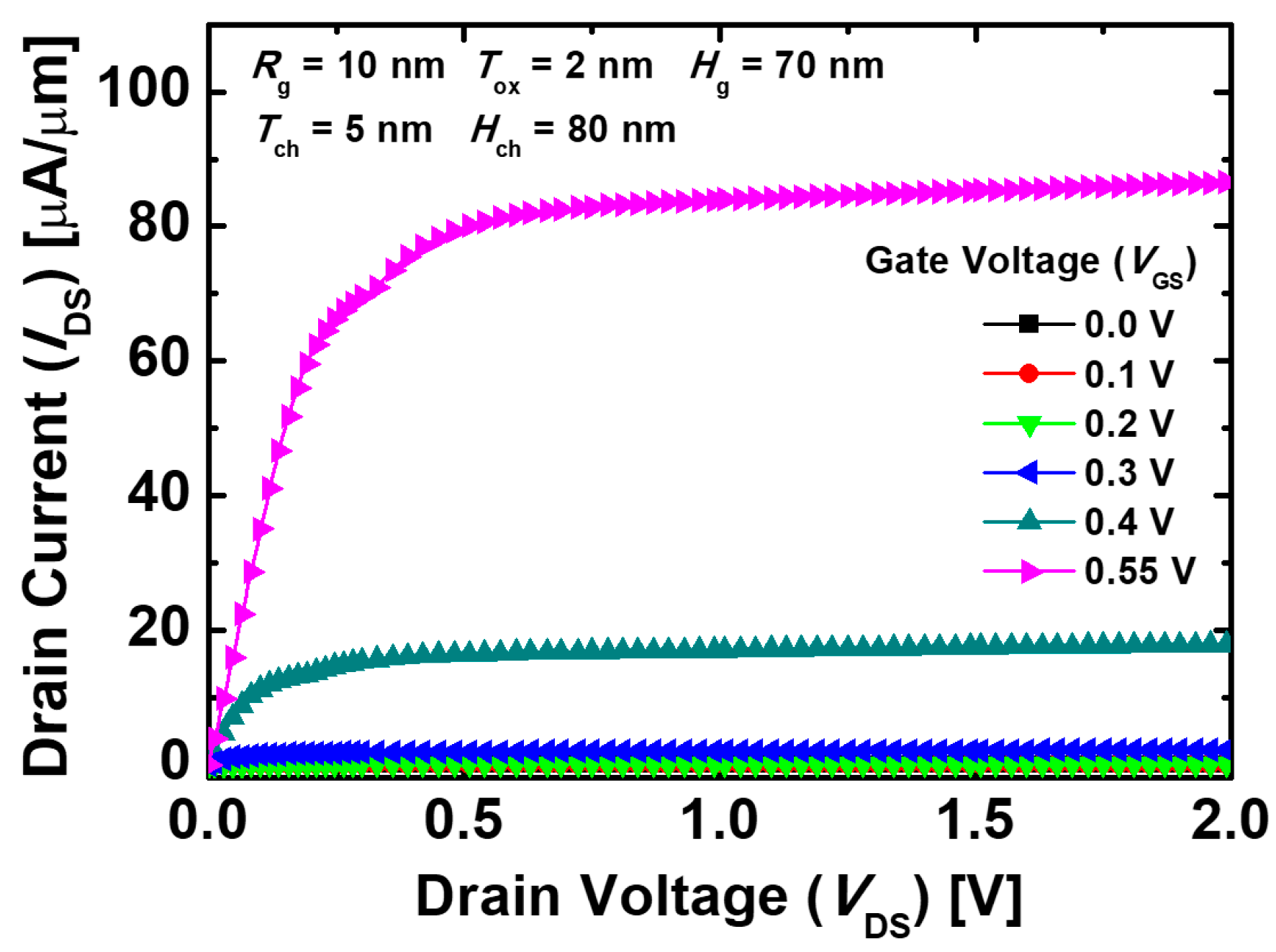
Figure 8 indicates the output characteristics of the proposed devices with different VGS. When a small VGS of 0.3 V or less is applied, IDS is almost constant and has a low value. IDS has a low value even though VDS increases because the amount of the electrons tunneled from the source to the channel region is small for a low VGS. When VGS is greater than 0.4 V, the tunneled electrons in the channel region drift toward the drain region by the positive VDS. IDS increases as a function of VDS for small VDS, then gets saturated and becomes less dependent on VDS when VDS is approximately 0.5 V, showing the proper output characteristics for circuit applications.
The comparison of the proposed device with the different works in terms of Ion, Vt, VDD, and SS is presented in Table 1. This proposed device has the highest Ion value with the low Vt and the low VDD value. Thus, the proposed Ge-based gate-metal-core VNWTFET is a suitable candidate for the logic devices with the low power consumption.

4. Conclusions

In this work, a Ge-based gate-metal-core VNWTFET was optimally designed and analyzed based on TCAD simulations. With wider BTBT junctions, a higher current drivability can be realized compared to the conventional TFETs. The proposed device demonstrated superior DC performances with Ion = 8.09 × 10⁻⁵ A/μm, Ioff = 1.09 × 10⁻¹² A/μm, Vt = 0.21 V, Ion/Ioff = 7.45 × 10⁷, and SS = 42.8 mV/dec at Hg = 70 nm, Tch = 5 nm, and Hch = 80 nm. It is ensured that the proposed device would be a promising logic device for the low-power applications.

Author Contributions

Conceptualization, W.D.J.; Investigation, W.D.J., J.H.J. and S.H.L.; Data analysis, W.D.J., Y.J.Y., M.S.C., J.J. and J.-H.B.; writing—original draft preparation, W.D.J.; writing—review and editing, I.M.K.

Funding

This work was supported by the National Research Foundation of Korea (NRF) grant funded by the Korea government (MSIT) (No. NRF-2019R1H1A1080165) and in part by Samsung Electronics Co. Ltd. This study was also supported by the BK21 Plus project funded by the Ministry of Education, Korea (21A20131600011). This work was also supported by the Ministry of Trade, Industry & Energy (MOTIE) (10080513). This work was supported by NRF grant funded by the Korean government (NRF-2018H1A2A1063117-Global Ph. D. Fellowship Program).

Acknowledgments

Korea Semiconductor Research Consortium (KSRC) support program for the development of the future semiconductor devices. The EDA tool was supported by the IC Design Education Center (IDEC), Korea.

Conflicts of Interest

The authors declare no conflict of interest.

References

  1. Avci, U.E.; Rios, R.; Kuhn, K.; Young, I.A. Comparison of performance, switching energy and process variations for the TFET and MOSFET in logic. In Proceedings of the 2011 Symposium on VLSI Technology-Digest of Technical Papers, Honolulu, HL, USA, 14–16 June 2011; pp. 124–125. [Google Scholar]
  2. Davari, B.; Dennard, R.H.; Shahidi, G.G. CMOS scaling for high performance and low power-the next ten years. Proc. IEEE 1995, 83, 595–606. [Google Scholar] [CrossRef] [Green Version]
  3. Khatami, Y.; Banerjee, K. Steep subthreshold slope n- and p-type tunnel-FET devices for low-power and energy-efficient digital circuits. IEEE Trans. Electron Devices 2009, 85, 2752–2761. [Google Scholar] [CrossRef]
  4. Choi, W.Y.; Park, B.G.; Lee, J.D.; Liu, T.J.K. Tunneling field-effect transistors (TFETs) with subthreshold swing (SS) less than 60 mV/dec. IEEE Electron Device Lett. 2007, 28, 743–745. [Google Scholar] [CrossRef]
  5. Nirschl, T.; Wang, P.F.; Weber, C.; Sedlmeir, J.; Heinrich, R.; Kakoschke, R.; Schrufer, K.; Holz, J.; Pacha, C.; Schulz, T.; et al. The tunneling field effect transistor (TFET) as an add-on for ultra-low-voltage analog and digital processes. In Proceedings of the 2004 IEEE International Electron Devices Meeting (IEDM), San Francisco, CA, USA, 13–15 December 2004; pp. 195–198. [Google Scholar]
  6. Wang, P.F.; Hilsenbeck, K.; Nirschl, T.; Oswald, M.; Stepper, C.; Weis, M.; Schmitt-Landsiedel, D.; Hansch, W. Complementary tunneling transistor for low power application. Solid-State Electron. 2004, 48, 2281–2286. [Google Scholar] [CrossRef]
  7. Avci, U.E.; Kuhn, K.J.; Young, I.A. Comparison of power and performance for the TFET and MOSFET and considerations for P-TFET. In Proceedings of the 2011 11th IEEE International Conference on Nanotechnology, Portland, OR, USA, 15–18 August 2011; pp. 869–872. [Google Scholar]
  8. Vladimirescu, A.; Amara, A.; Anghel, C. An analysis on the ambipolar current in Si double-gate tunnel FETs. Solid-State Electron. 2012, 70, 67–72. [Google Scholar]
  9. Moselund, K.E.; Ghoneim, H.; Bjork, M.T.; Schmid, H.; Karg, S.; Lortscher, E.; Riess, W.; Riel, H. Comparison of VLS grown Si NW tunnel FETs with different gate stacks. In Proceedings of the 2009 European Solid State Device Research Conference, Athens, Greece, 14–18 September 2009; pp. 448–451. [Google Scholar]
  10. Narang, R.; Saxena, M.; Gupta, R.S.; Gupta, M. Assessment of ambipolar behavior of a tunnel FET and influence of structural modifications. J. Semicond. Technol. Sci. 2012, 12, 482–491. [Google Scholar] [CrossRef]
  11. Wan, J.; Le, R.C.; Zaslavsky, A.; Cristoloveanu, S. Tunneling FETs on SOI: Suppression of ambipolar leakage, low-frequency noise behavior, and modeling. Solid-State Electron. 2011, 65, 226–233. [Google Scholar] [CrossRef]
  12. Krishnamohan, T.; Kim, D.; Raghunathan, S.; Saraswat, K. Double-gate strained-Ge heterostructure tunneling FET (TFET) with record high drive currents and ≪60mV/dec subthreshold slope. In Proceedings of the 2008 IEEE International Electron Devices Meeting (IEDM), San Francisco, CA, USA, 15–17 December 2008; pp. 1–3. [Google Scholar]
  13. Schenk, A.; Sant, S.; Moselund, K.; Riel, H. III–V-based hetero tunnel FETs: A simulation study with focus on non-ideality effects. In Proceedings of the 2016 Joint International EUROSOI Workshop and International Conference on Ultimate Integration on Silicon (EUROSOI-ULIS), Vienna, Austria, 25–27 January 2016; pp. 9–12. [Google Scholar]
  14. Hu, V.P.; Wang, C. Optimization of III–V heterojunction tunnel FET with non-uniform channel thickness for performance enhancement and ambipolar leakage suppression. Jpn. J. Appl. Phys. 2018, 57, 04FD18. [Google Scholar] [CrossRef]
  15. Dubey, P.K.; Kaushik, B.K. T-Shaped III-V Heterojunction Tunneling Field-Effect Transistor. IEEE Trans. Electron Devices 2017, 64, 3120–3125. [Google Scholar] [CrossRef]
  16. Walke, A.M.; Vandooren, A.; Rooyackers, R.; Leonelli, D.; Hikavyy, A.; Loo, R.; Verhulst, A.S.; Kao, K.; Huyghebaert, C.; Groeseneken, G.; et al. Fabrication and analysis of a Si/Si0.55Ge0.45 Heterojunction Line Tunnel FET. IEEE Trans. Electron Devices 2014, 61, 707–715. [Google Scholar] [CrossRef]
  17. Nah, J.; Liu, E.S.; Varahramyan, K.M.; Tutuc, E. Ge-SixGe1−x core-shell nanowire tunneling field-effect transistors. IEEE Trans. Electron Devices 2010, 57, 1883–1888. [Google Scholar] [CrossRef]
  18. Shih, P.C.; Hou, W.C.; Li, J.Y. A U-gate InGaAs/GaAsSb heterojunction TFET of tunneling normal to the gate with separate control over ON- and OFF-state current. IEEE Electron Device Lett. 2017, 38, 1751–1754. [Google Scholar] [CrossRef]
  19. Yang, Z. Tunnel field-effect transistor with an L-shaped gate. IEEE Electron Device Lett. 2016, 37, 839–842. [Google Scholar] [CrossRef]
  20. Seo, J.H.; Yoon, Y.J.; Lee, S.; Lee, J.H.; Cho, S.; Kang, I.M. Design and analysis of Si-based arch-shaped gate-all-around (GAA) tunneling field-effect transistor (TFET). Curr. Appl. Phys. 2015, 15, 208–212. [Google Scholar] [CrossRef]
  21. Bagga, N.; Kumar, A.; Dasgupta, S. Demonstration of a novel two source region tunnel FET. IEEE Trans. Electron Devices 2017, 64, 5256–5262. [Google Scholar] [CrossRef]
  22. Imenabadi, R.M.; Saremi, M.; Vandenberghe, W.G. A novel PNPN-like Z-shaped tunnel field-effect transistor with improved ambipolar behavior and RF performance. IEEE Trans. Electron Devices 2017, 64, 4752–4758. [Google Scholar] [CrossRef]
  23. Ko, E.; Lee, H.; Park, J.D.; Shin, C. Vertical tunnel FET: Design optimization with triple metal-gate layers. IEEE Trans. Electron Devices 2016, 63, 5030–5035. [Google Scholar] [CrossRef]
  24. Yoon, J.S.; Kim, K.; Meyyappan, M.; Baek, C.K. Bandgap engineering and strain effects of core-shell tunneling field-effect transistors. IEEE Trans. Electron Devices 2018, 65, 277–281. [Google Scholar] [CrossRef]
  25. Hu, C. Modern Semiconductor Devices for Integrated Circuits, International ed.; Prentice Hall: Upper Saddle River, NJ, USA, 2009; p. 206. [Google Scholar]
  26. Sentaurus User’s Manual; Version L-2016.03; Synopsys Inc.: Mountain View, CA, USA, 2016.
  27. Martino, M.D.; Martino, J.A.; Agopian, P.G. Drain induced barrier tunneling on TFETs with different source/drain engineering. In Proceedings of the 2014 29th Symposium on Microelectronics Technology and Devices (SBMicro), Aracaju, Brazil, 1–5 September 2014; pp. 1–4. [Google Scholar]
  28. Patel, J.; Sharma, D.; Yadav, S.; Lemtur, A.; Suman, P. Performance improvement of nano wire TFET by hetero-dielectric and hetero-material: At device and circuit level. Microelectron. J. 2019, 85, 72–82. [Google Scholar] [CrossRef]
  29. Kumar, N.; Mushtaq, U.; Amin, S.I.; Anand, S. Design and performance analysis of Dual-Gate All around Core-Shell Nanotube TFET. Superlattice Microstruct. 2019, 125, 356–364. [Google Scholar] [CrossRef]
  30. Li, W.; Wang, S.; Chen, S.; Yang, Z. Design of High performance Si/SiGe Heterojunction Tunneling FETs with a T-Shaped Gate. Nanoscale Res. Lett. 2017, 12, 198. [Google Scholar] [CrossRef] [PubMed]
  31. Vanlalawmpuia, K.; Bhowmick, B. Investigation of a Ge-Source Vertical TFET with Delta-Doped Layer. IEEE Trans. Electron Devices 2019, 66, 4439–4445. [Google Scholar] [CrossRef]
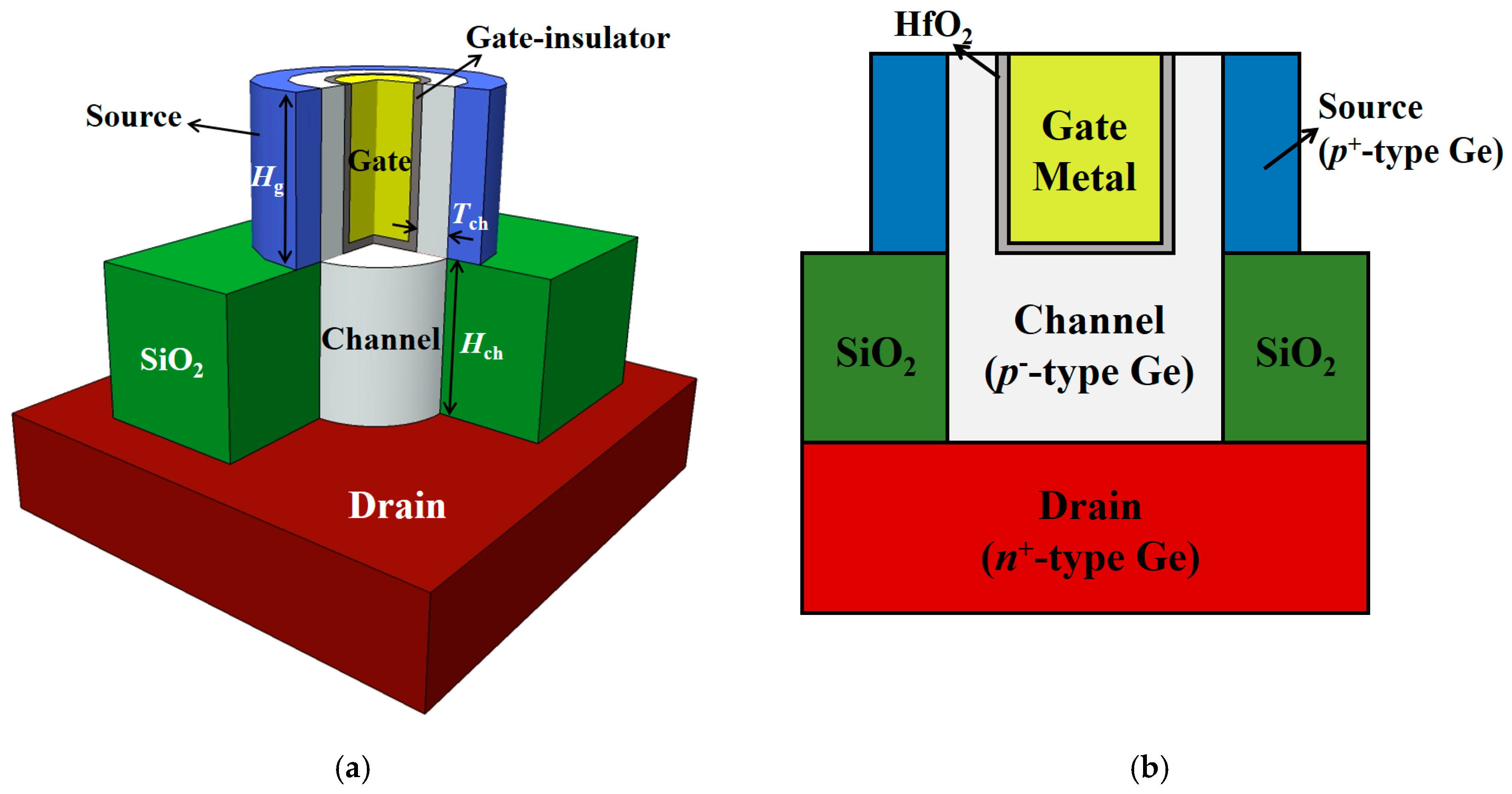
Figure 1. (a) Schematic view and (b) cross-sectional view of the proposed Ge-based gate-metal-core vertical nanowire tunnel field effect transistor (VNWTFET), respectively.
Micromachines 10 00749 g001
Figure 2. (a) The electron flow and (b) energy band diagrams of the proposed Ge-based gate-metal-core VNWTFETs. Energy band diagrams are extracted across the A–A’ line in Figure 2a.
Micromachines 10 00749 g002
Figure 3. (a) IDSVGS (drain current–gate voltage) transfer characteristics and (b) energy band diagrams of the proposed devices with different channel thicknesses (Tch). The energy band diagrams are extracted across the A–A’ line in Figure 2a.
Micromachines 10 00749 g003
Figure 4. Ion and subthreshold swing (SS) characteristics of the proposed Ge-based gate-metal-core VNWTFETs with different Tch.
Micromachines 10 00749 g004
Figure 5. (a) IDSVGS transfer characteristics and (b) Ion/Ioff (on-state current/off-state current) and SS of the proposed Ge-based gate-metal-core VNWTFETs with different gate-metal heights (Hg).
Micromachines 10 00749 g005
Figure 6. (a) IDSVGS transfer characteristics and (b) energy band diagrams of the proposed Ge-based gate-metal-core VNWTFETs with different channel heights (Hch). The energy band diagrams are extracted across the B–B’ line in Figure 2a at VGS = −0.55 V and VDS = 0.55 V (drain voltage).
Micromachines 10 00749 g006
Figure 7. Ion and SS characteristics of the proposed Ge-based gate-metal-core VNWTFETs with different Hch.
Micromachines 10 00749 g007
Figure 8. Output characteristics of the proposed Ge-based gate-metal-core VNWTFETs with different VGS.
Micromachines 10 00749 g008
Table 1. Comparison with the different works.
ParameterThis WorkSiGe-S-NW-TFET [28]Si-Based Nanotube TFET [29]Si/SiGe HTG-TFET [30]Ge-Source vTFET [31]
Ion (μA/μm)80.9 (at VGS = 0.55 V)11.66 (at VGS = 1.0 V)5.0 (at VGS = 1.5 V)7.02 (at VGS = 0.5 V)27.6 (at VGS = 0.5 V)
Vt (V)0.210.370.90.280.20
VDD (V)0.550.81.20.50.5
SS (mV/dec)42.823.7558.344.6421.2