Abstract
The paper presents the results concerning the influence of the thickness of the ITO and In2O3 layers deposited by the magnetron sputtering method on the physical parameters characterising their surface properties. The characterisation parameters were obtained by atomic force microscopy (AFM), X-ray photoelectron spectroscopy (XPS), and Kelvin probe. The increase in the layers’ thickness related to the time of their fabrication causes an increase in the surface roughness and the value of the work function, followed by a decrease in the concentration of elements and compounds in the near-surface area.
1. Introduction
One can find several definitions in the literature about contact potential, photo electricity, thermal emission of electrons, and band theory of electrical conductivity. It is possible to determine the work function of the other conductor by measuring the contact voltage, i.e., the voltage between the surface of the two conductors, knowing the work function for one of the conductors. The contact potential measurement can be performed in two ways [1,2,3,4,5,6,7].
The first one concerns the measurement of the contact value of the contact potential difference (CPD) with the reference electrode (RE) at the Kelvin probe stand and then the calculation of the work of the electron work function (Φ). Knowing the parameter Φ enables defining the Fermi level for the tested material (e.g., semiconductor). Concerning the material, it is also necessary to determine the type and condition of its surface. Such factors include temperature, type and thickness of the adsorbate, and ionisation of element atoms. The structure of the Kelvin Probe includes an electric circuit with a regulated voltage source connected, an ammeter, and a vibrating ER electrode above the test sample. A reference electrode (usually made of a golden mesh) is used [8] to eliminate the material oxidation process and change its work function. In work [8], this concept was defined as the value of the difference between the work function of the gold vibrating electrode RE and the work function of the tested sample divided by the elementary charge, where the electric capacity of sample C is equal to the Q charge accumulated on the sample (Table 1) [8].

Table 1.
Formulae and quantities characterising the tested sample’s work function [8,9,10,11].
The study used indium tin oxide (ITO), which is commonly known as n-type transparent conductive oxide (TCO). It combines good electrical conductivity with optical transparency in the visible range [12,13,14]. It is widely used as a high-work function electrode for optoelectronic applications such as solar cells or organic light-emitting diodes (OLED) [15,16]. Moreover, transparent conducting oxides (TCOs) are essential materials used in flat panel displays, photovoltaics, and electrochromic windows [17]. These papers [18,19,20,21,22,23,24] show the determination of the work function of commercially available and surface-modified ITO substrates using the Kelvin probe.
The issue of the contact potential difference (CPD) method with the use of a Kelvin probe for the application of thin layers of transparent conductive oxides (TCO) was analysed also based on data contained in the “Elsevier (Science Direct)”, Web of Science, and Scopus databases. Table 2 shows that the Elsevier database recorded the most significant number of published works for all the issues searched except for one. The WOS database took second place, and the Scopus database was third in terms of the analysed issues. Based on the available literature resources from these databases in the years 1968 to 2020 for the WOS base, 1960 to 2020 for the Scopus lilac, and 1998 to 2020 for the Elsevier base, it can be stated that this is a topic that scientists have been interested in for a long time (state of knowledge as of 28 March 2022).
Table 2.
List of published publications on general topics by three databases [22,23,24].
Table 3 summarises the results of specific issues in two WOS and Scopus databases from 2020. It can be concluded that a more significant number of published works related to issues related to background oxides are contained in the WOS database than in Scopus (the state of knowledge as of 4 May 2022). Analysing the obtained research results since information technology’s development, the creation of bibliographic lists has been moved to the virtual space, thanks to which the considered issues can be presented statistically. Databases help an increasing number of emerging scientific journals, which separate valuable scientific publications from those of poor quality of those that are unscientific.
Table 3.
List of published publications according to two databases, taking into account specific issues [23,24].
The investigation is based on experimental results of the In2O3 and ITO thin film samples, usually polycrystalline, highly defective layers produced by magnetron sputtering. To probe the potential of In2O3 and ITO for contact layers in thin solar cells based on metal oxides (e.g., CuO), which is the future aim of our works, it is necessary to investigate the electronic structure and properties of both thin layers. This work is a series of publications on this topic. Obtaining a ready electronic structure with the highest efficiency value is possible by the mutual correlation of parameters with layers created in the optimized technological process of its manufacturing. The mentioned correlation is important in the technology of their products because various processes take place during their manufacture, which can cause both an increase and a decrease in the desired external parameters of the electronic structure. The decline may be due to the degradation of the physical parameters of the layers of the electronic structure. It belongs to the decisive following parameters [25]: electromagnetic radiation reflection coefficient, solar cell base material thickness, charge carrier concentration and its mobility, charge carrier effective lifetime, carrier diffusion path length charge, surface recombination speed, electromagnetic radiation absorption coefficient, spectral sensitivity, resistances of areas and structural elements of the solar cell, type, and concentration of defects and the resulting density of recombination centers. Electrical optical, and structural properties are integral measurements of the whole material. This paper does not present the results concerning the examination of the optical properties of the discussed materials as they were included in earlier papers [26,27].
2. Materials for Investigation
The magnetron sputtering method was applied to the deposition ITO and In2O3 layers. A constant current value (100 W) determining the set power was used for the samples. The thickness of the applied layers was also changed from 15 to 135 nm. The layering rate was monitored with a quartz microbalance. Into the investigation were applied p-type Cz-Si wafers ((100) orientation) with a thickness of 380 μm ± 25 μm and resistivity of 7.5–8 Ωcm. Borosilicate optical glasses and two ITO targets, suitable for producing mixed indium tin oxide (ITO) layers with a composition-dependent resistivity, were used for the tests. In this work, the following alloy composition was applied: In and Sn alloy type, 99.99% purity and 99:10 (wt.%). Preparation of samples for investigation included: silicon wafers, which were subjected to chemical etching processes, and optical glasses, which were chemically washed in an ultrasonic cleaner.
3. Methodology
Measurement of the contact value of the contact potential difference (CPD) investigated samples concerning the reference electrode (RE) (for gold of 4.815 eV) was performed on a Kelvin probe, and then work function (Φ) was calculated. The thickness of thin layers was measured at the Sentech SE 800PV spectral ellipsometer(Berlin, Germany) based on the Step Scan Analyzer measurement mode. Measurements were in the range of 240–980 nm, and the angles of incidence were 50, 60, and 70 degrees. To study the morphology of the investigated samples (the roughness) a Park System XE-100 (Suwon, Korea) atomic force microscope was used. A non-contact mode was applied with a probe elastic constant of 40 N/m and a resonance frequency of 300 kHz. The investigations were performed in the area of 10 × 10 and 1 × 1 micrometres. The X-ray photoelectron spectra (XPS) were acquired using hemispherical analyser EA 15 (PREVAC) equipped with dual anode X-ray source RS 40B1 (PREVAC, Brzeziny, Poland). The measurements were performed using Al Kα (1486.6 eV) radiation and an analyser pass energy of 100 eV. The spectra were recorded in normal emission geometry with an energy resolution of 0.9 eV. The binding energy scale of the analyzer was calibrated concerning Au 4f7/2 (84.0 eV) region of the gold-covered sample placed at the same sample stage [28]. The ultra-high vacuum (UHV) conditions of 8 × 10⁻¹⁰ mbar were maintained during the measurements. The analysis area was approximately 3 mm2, and the depth of analysis was about 10 nm. The spectra were analysed with the use of CasaXPS 2.3.24 software(Casa Software Ltd, Devon, United Kingdom). The electron binding energy (BE) scale was calibrated for the Fermi edge at 0.0 eV. The Shirley-type spectrum background was used.
Spectra were fitted using CASA XPS® software with the use of embedded algorithms. If not specified, the components were fitted with a product of Gauss (30%) and Lorenz (70%). The spectra were compared to the background level.
4. Results and Discussion
Kelvin probe work function and thickness analysis were used. Using a Kelvin probe, the CPD was measured for the thin layers of In2O3 and ITO deposited by the magnetron sputtering technique on glass substrates. Each sample was measured in several places. Table 4 presents the Φ results of the obtained layers.
Table 4.
The results of the work function, thickness, and roughness of the investigated samples [7,8,9,10].
The work function for each sample was calculated based on the investigation results. For the indium oxide layer, no significant differences were observed in the calculated value of ϕ for different thicknesses. The experimentally determined work function for deposited In2O3 is about 4.6 eV, while the literature value is about 5 eV [29]. In the case of indium-doped tin oxide, the ϕ values seem to depend to some extent on the thickness of the layer. The highest work function among the measured oxides was shown by indium tin oxide for the thickest layers (70 and 100 nm), while indium oxide showed the lowest value for the layer thickness of 20 nm. Higher work function values of ITO layers compared to the value of the reference sample result from network defects. Thin layers are characterised by a lower work function value (4.33 eV for 25 nm and 4.37 eV for 45 nm), which may result from their surface composition and/or defects. Thicker layers (especially 135 nm) are characterised by the work function close to the theoretical value of 4.7–4.8 eV. The work function of the commercial ITO (Ossilla-product Code S111) reference sample was 4.85 eV.
AFM analysis is considered next. The topography of the deposited layers was investigated by AFM and presented in Figure 1 and Figure 2. Based on obtained In2O3 and ITO results, it was found that the layers with the most negligible thickness have a finer-crystalline structure than the layers with the most significant thickness. The results showed that ITO and In2O3 thin layers have a crystalline structure with a domain that increases in size with increasing thickness. Grown layers’ completeness depends on the quality of interfaces, which in turn depends on the number of properties, such as crystal structure and defects existing in a thin layer. Parameters, such as thickness, doping type, level, and other deposited conditions, should be optimized to optimize electrical parameters—for instance, the potential of the contact layer, low electrical resistance, as well optical parameters such as high transparency [30]. The roughness measurements showed an increase in In2O3 and ITO roughness with the layer thickness (Table 4).
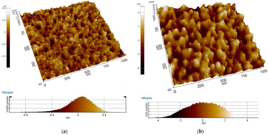
Figure 1.
Topography of the applied In2O3 layers with thickness (a) 25 nm, (b) 135 nm (chosen example) (AFM).
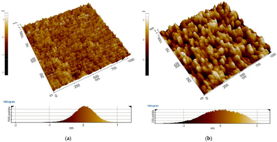
Figure 2.
Topography of the applied ITO layers with thickness (a) 25 nm, (b) 135 nm (chosen example) (AFM).
XPS analysis is next considered. The surface composition and electronic states of the elements were analyzed for the fabricated samples. The acquired spectra were deconvoluted, taking into account the lowest number of components possible, the full width at half maximum (FWHM) of the analyzed peaks related to physically possible values for the given elements, the analyser resolution, and the chemical composition of the samples.
Results for In2O3 and ITO are next considered. The results of In2O3 and ITO surface composition analysis on a basis of survey spectra are collected in Table 5 and Figure 3. The performed analysis shows that In2O3 layer of 135 nm is approximately twice more contaminated with the carbon species than the 25 nm sample. Such a result suggests that the In2O3 target is contaminated with carbon species, which are sputtered together with the main target component, i.e., In2O3. In case of ITO layers, the carbon contamination of the surfaces is independent of the deposition time. Moreover, the oxygen concentration remains constant for the same deposition conditions, which confirms that the sputtering targets of ITO and In2O3 are different.
Table 5.
The results of survey spectra of In2O3 and ITO sample surfaces samples.
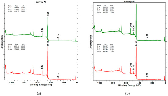
Figure 3.
Survey spectra of (a) In2O3, (b) ITO sample surfaces (where: at the bottom −25 nm, at the top 135 nm).
An analysis of the high-resolution spectra for In2O3 sample (Figure 4) corroborate the conclusion on a basis of survey spectra analysis.
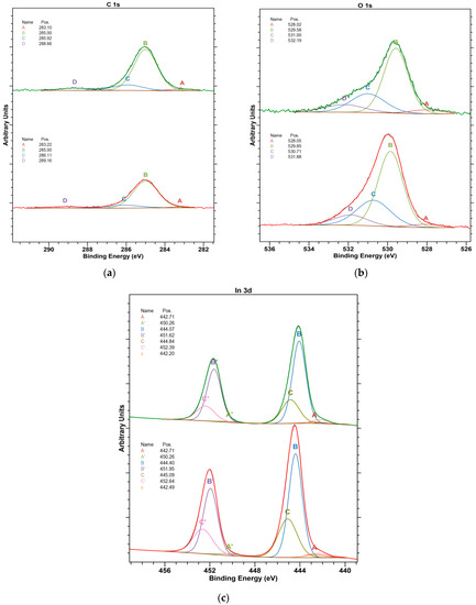
Figure 4.
High-resolution XP spectra of In2O3layers (a) C 1s (A: C-metal; carbon-metal bonding, carbides, B: C-C; organic carbon, the BE suggests that it can be sp2 in majority, C: C-O; alcohol or ether groups, D: COOH, carboxylic or peptide groups), (b) O 1s (A: O-metal, defected oxide structure, presence of oxygen vacancies, B: O-metal, lattice oxides, C: OH, hydroxyl groups at the surface, D: O-C + H2O, organic compounds and water, oxygen bonded to short aliphatic chains + adsorbed water), (c) In 3d (A: In-C; surface carbides, B: In3+-O; In2O3 lattice oxide, C: In3+-OH; In(OH)3) (where: name-spectrum component (in case of doublet excitation, the maxima are depicted as A and A’, etc.).
The high-resolution spectra for ITO samples are collected in Figure 5a.
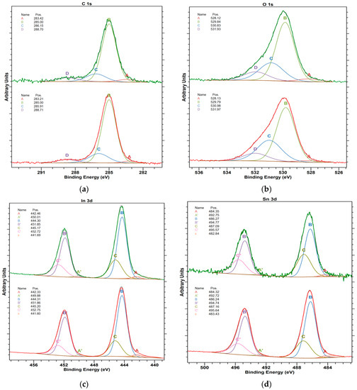
Figure 5.
High-resolution XP spectra of ITO layers (a) C 1s (A: C-metal; carbon-metal bonding, carbides, B: C-C; organic carbon, the BE suggests that it can be sp2 in the majority, C: C-O; alcohol or ether groups, D: COOH, carboxylic or peptide groups), (b) O 1s (A: O-metal, defected oxide structure, presence of oxygen vacancies, B: O-metal, lattice oxides, C: OH, hydroxyl groups at the surface, D: O-C + H2O, organic compounds and water, oxygen bonded to short aliphatic chains + adsorbed water), (c) In three dimensions (A: In-C; surface carbides, B: In3+-O; In2O3 lattice oxide, C: In3+-OH; In(OH)3, (d) Sn 3d spectra of 25 nm ITO (bottom) and 135 nm ITO (top) sample surfaces (A: Sn-C, tin carbides, B: Sn4+-O; SnO2, C: Sn4+-OH; Sn(OH)4).
The deconvolution of C 1s spectra shows four spectrum components, where the one at lowest electron binding energy (BE) of app. 283 eV is assigned to carbon–metal bonding (Figure 4a). The amount of carbon–metal bonds increases with the layer thickness. This suggests the presence of carbide species at the surface of deposited layers and supports the conclusion that these species result from the target composition, i.e., from bonding agent of In2O3 powder in the target body. The O 1s spectra acquired at both studied surfaces show the presence of oxygen vacancies (component A) (Figure 4b). The amount of vacancies increases with the layer thickness, which suggests that the vacuum conditions applied during the deposition process have an impact on vacancy formation. On the other hand, the main surface component is still a lattice oxide, as indicated by B component of O 1s spectra. Based on the analysis of In 3d (Figure 4c), where the spectrum shows three doublet components, it can be stated that the main surface component is oxide. The surfaces of In2O3 contain hydroxyl groups (component C), which is in good agreement with O 1s spectra.
The deconvolution of C 1s spectrum confirms that similar carbon species are found on both studied surfaces independently of the thickness. Similarly to C 1s, the O 1s core excitations (Figure 5b) for both studied surfaces show limited difference and presence of oxygen vacancies (component A). The amount of vacancies slightly increases with the layer thickness. The In 4d spectrum (Figure 5c) shows three doublet components, where the most intensive one is ascribed to the lattice indium oxide. The surfaces of In2O3 also contain hydroxyl groups (component C), which are in good agreement with O 1s spectra. Based on the analysis of Figure 5d for Sn 4d spectra, three electronic states of tin are found on the studied surfaces. The most intensive peak (B) can be ascribed to tin(IV) bonded to oxygen in SnO2 structures. The thinner film shows lower intensity of the peaks assigned to hydroxyl groups (component C), which can be well related to increasing surface roughness (surface development) with the layer thickness.
5. Conclusions
The material parameters of the individual layers of the electronic structure have a decisive influence on the electrical parameters of the solar cell. The material parameters include the type, thickness, and density of the anti-reflective layer electronic structure, paste composition (metallic material, organic carriers, and oxides), surface morphology, and other metallic layers, electronic structures, and distribution profile emitter admixture–dopant concentrations in the near-surface area. Technological parameters include-temperature distribution as a function of stage time drying, temperature–time distribution of the contact-making step paste-substrate, distribution of temperature as a function of time of the electronic structure cooling stage and pastes, gas composition, flow in heating zones, and sources temperature in the reactor. Obtaining a photovoltaic cell with the highest efficiency value is possible by the mutual correlation of the aforementioned parameters.
As can be seen from the measurements using the Kelvin probe, the work function Φ of In2O3 does not depend on the layer thickness, and it is at the level of 4.6 eV. This is in contrast to ITO, for which the Φ increases with layer thickness change in the range from 25 nm to 135 nm. The work function for the thickest ITO layer is 4.8 eV, which corresponds to the commercial products. AFM analysis reveals that the crystalline structure of investigated samples strongly depends on the thickness of the deposited layers. Not just the thickness, but also the optimization of doping concentration, can also influence the selection of particular grain sizes. X-ray photoelectron spectrometry (XPS) was performed to analyze the surface composition of the obtained layers. Based on the survey spectra analysis of In2O3, it was found that the sample with the thicker layer is twice more contaminated with the carbon species than a sample with a thinner layer. Based on the survey spectra analysis of ITO, it was found that both surfaces are very similar in chemical composition.
6. Summary
Based on the research results, it was found that:
- From the measurements using the Kelvin probe, the work function Φ of In2O3 does not depend on the layer thickness, while the work function Φ of ITO seems to depend on the thickness of the layer.
- The results of coating morphology investigations with the use of AFM show the dependence of the coating structure on thickness. It was found that thinner coatings have a structure with a smaller grain size than thicker coatings. It proves that the grains of the tested coating material grow along with the increasing thickness of the coating. Similar phenomena were explained in other works by the Ostwald-Lussac law, for example, in the work [31].
- The Kelvin probe equipped with a light source allows for testing the surface conditions of samples. For example, in photovoltaic materials, surface states play an important role in charge transfer. The depth of analysis of the investigated material is about 2 nm for the Kelvin probe and about 10 nm for XPS. The XPS method shows high sensitivity surface, which comes down to a small analytical depth, which, in the case of metals, is about 5 nm.
- Obtaining a photovoltaic cell with the highest efficiency value is possible by the mutual correlation of the material and technological parameters. The work function, valence band maximum, and electronic states in the band gap are other parameters that need to be investigated in In2O3 and ITO layers, which is also the future aim of the author’s works. We are going to discuss changes in the electronic structure induced by the defects to evaluate the applicability of band gap corrections.
Author Contributions
Conceptualization, M.M.-S. and P.P.; methodology, M.M.-S.; validation, M.M.-S., R.S. and K.G.-N.; formal analysis, M.M.-S.; investigation, M.M.-S., R.S. and K.G.-N.; writing—original draft preparation, M.M.-S. and P.P.; writing—review and editing, M.M.-S. and P.P.; funding acquisition, M.M.-S. All authors have read and agreed to the published version of the manuscript.
Funding
Publication supported under the Rector’s pro-quality grant. Silesian University of Technology, grant number: 10/050/RGJ22/1028.
Institutional Review Board Statement
Not applicable.
Informed Consent Statement
Not applicable.
Data Availability Statement
Not applicable.
Conflicts of Interest
The authors declare no conflict of interest.
References
- Schroder, D.K. Semiconductor Material and Device Characterisation, 3rd ed.; Wiley-IEEE Press: Hoboken, NJ, USA, 2006; ISBN 9780471749080. [Google Scholar]
- Wojas, W.; Wojas, J. Part II: The Main Measurement Methods of Physical Surface Parameters. In Physical Parameters of Solid Surfaces and Their Dependence on the Outside Conditions; Universal Decimal Classification: The Hague, The Netherlands, 2009; pp. 391–405. [Google Scholar]
- Li, M.; Wang, Y.; Tian, N.; Huang, H. Heterojunction and ferroelectric polarisation co-promoting photocatalytic activity. Appl. Surf. Sci. 2022, 587, 1–11. [Google Scholar] [CrossRef]
- Zhukov, A.A.; Bozhko, S.I.; Eliseev, A.A. Measurements of the work function of AgI intercalated carbon nanotubes using different scanning techniques. Phys. E Low Dimens. Syst. Nanostruct. 2022, 135, 114943. [Google Scholar] [CrossRef]
- Yue, X.; Cheng, L.; Fan, J.; Xiang, Q. 2D/2D BiVO4/CsPbBr3 S-scheme heterojunction for photocatalytic CO2 reduction: Insights into structure regulation and Fermi level modulation. Appl. Catal. B Environ. 2022, 304, 120979. [Google Scholar] [CrossRef]
- Singh, R.; Dutta, A.; Basu, N.; Lahiri, J.; Som, T. Improved photovoltaic performance of CdTe-based solar cells: Roles of using a hole-blocking layer and nanoscale imaging of barrier height at interfaces. Sol. Energy 2021, 215, 1–11. [Google Scholar] [CrossRef]
- Elakia, M.; Gobinath, M.; Sivalingam, Y.; Palani, E.; Ghosh, S.; Nutalapati, V.; Surya, V.J. Investigation on visible light assisted gas sensing ability of multi-walled carbon nanotubes coated with pyrene based organic molecules. Phys. E Low Dimens. Syst. Nanostruct. 2020, 124, 114232. [Google Scholar] [CrossRef]
- Gawlińska-Nęcek, K.; Majchrowicz, Ł.; Starowicz, Z.; Wlazło, M.; Putynkowski, G.; Socha, R.; Panek, P. Innovative Methods of Production of Photovoltaic Cells and Modules, Publisher; Attyka: Warsaw, Poland, 2021; p. 119. [Google Scholar]
- Riviere, J.C. Work Function: Measurements and Results. In Solid State Surface Science; Decker: New York, NY, USA, 1969. [Google Scholar]
- Hansen, W.N.; Hausen, G.J. Standard reference surfaces for work function measurements in air. Surf. Sci. 2001, 481, 172–184. [Google Scholar] [CrossRef]
- Wojas, J. Physics of Semiconductor Surfaces; PLJ: Warsaw, Poland; Academic Publishing House: Warsaw, Poland, 1995. [Google Scholar]
- Ciszewski, A.; Kiejna, A. The Work Function in Metals; University of Wroclaw: Wroclaw, Poland, 1986. [Google Scholar]
- Hamberg, I.; Granqvist, C.G. Evaporated Sn-doped In2O3 films: Basic optical properties and applications to energy-efficient windows. J. Appl. Phys. 1986, 60, R123–R159. [Google Scholar] [CrossRef]
- Hung, L.S.; Chen, C.H. Recent progress of molecular organic electroluminescent materials and devices. Mater. Sci. Eng. R Rep. 2002, 39, 143–222. [Google Scholar] [CrossRef]
- Tak, Y.H.; Kim, K.B.; Park, H.G.; Lee, K.H.; Lee, J.R. Criteria for ITO (Indium–Tin–Oxide) thin film as the bottom electrode of an organic light emitting diode. Thin Solid Film 2002, 411, 12–16. [Google Scholar] [CrossRef]
- Minami, T. Present status of transparent conducting oxide thin-film development for Indium-Tin-Oxide (ITO) substitutes. Thin Solid Film 2008, 516, 5822–5828. [Google Scholar] [CrossRef]
- Taylor, M.P.; Readey, D.W.; van Hest, M.F.A.M.; Teplin, C.W.; Alleman, J.L.; Dabney, M.S.; Gedvilas, L.M.; Keyes, B.M.; To, B.; Perkins, J.D.; et al. The Remarkable Thermal Stability of Amorphous In-Zn-O Transparent Conductors. Adv. Funct. Mater. 2008, 18, 3169–3178. [Google Scholar] [CrossRef]
- Chaney, J.A.; Koh, S.E.; Dulcey, C.S.; Pehrsson, P.E. Surface Chemistry of Carbon Removal from Indium Tin Oxide by Base and Plasma Treatment, with Implications on Hydroxyl Termination. Appl. Surf. Sci. 2003, 218, 258–266. [Google Scholar] [CrossRef]
- Chaney, J.A.; Pehrsson, P.E. Work function changes and surface chemistry of oxygen, hydrogen, and carbon on indium tin oxide. Appl. Surf. Sci. 2001, 180, 214–226. [Google Scholar] [CrossRef]
- Chen, S.H.; Bogaerts, A. Laser ablation of Cu and plume expansion into 1 atm ambient gas. J. Appl. Phys. 2005, 97, 063305. [Google Scholar] [CrossRef]
- Beerbom, M.M.; Lägel, B.; Cascio, A.J.; Doran, B.V.; Schlaf, R. Direct comparison of photoemission spectroscopy and in situ Kelvin probe work function measurements on indium tin oxide films. J. Electron Spectrosc. Relat. Phenom. 2006, 152, 12–17. [Google Scholar] [CrossRef]
- Available online: https://www-1sciencedirect-1com-1pjn01ni70007.han.polsl.pl (accessed on 28 March 2021).
- Available online: https://www-1scopus-1com-1gui8jpi70016.han.polsl.pl (accessed on 28 March 2021).
- Available online: https://www.webofscience.com (accessed on 28 March 2021).
- Szlufcik, J. Principles of Crystalline Silicon Solar Cells. In Photovoltaic and Photoactive Materials—Properties, Technology and Applications; Lecture in NATO Advanced Study Institute: Sozopol, Bulgaria, 2001. [Google Scholar]
- Musztyfaga-Staszuk, M.; Pudis, D.; Socha, R.; Gawlińska-Nęcek, K.; Panek, P. Optimised Magnetron Sputtering Method for the Deposition of Indium Tin Oxide Layers. Bull. Pol. Acad. Sci. Tech. Sci. 2021, 69, e139005. [Google Scholar]
- Musztyfaga-Staszuk, M.; Starowicz, Z.; Panek, P.; Socha, R.; Gawlińska-Nęcek, K. The Influence of Material Parameters on Optical and Electrical Properties of Indium-Tin Oxide (ITO) Layer. In Journal of Physics—Conference Series; IOP Publishing: Bristol, UK, 2020; Volume 1534, p. 012001. [Google Scholar]
- Lindau, I.; Pianetta, P.; Yu, K.Y.; Spicer, W.E. Photoemission of gold in the energy range 30–300 eV using synchrotron radiation. Phys. Rev. B 1976, 13, 492–495. [Google Scholar] [CrossRef]
- Pan, C.A.; Ma, T.P. CW carbon monoxide laser with microwave excitation in the supersonic flow. Appl. Phys. Lett. 1980, 37, 672–674. [Google Scholar]
- Parsianpour, E.; Raoufi, D.; Roostaei, M.; Sohrabi, B.; Samavat, F. Characterization and Structural Property of Indium Tin Oxide Thin Films. Adv. Mater. Phys. Chem. 2017, 7, 42–57. [Google Scholar] [CrossRef]
- Staszuk, M. Investigations of CrN+Cr2O3/TiO2 coatings obtained in a PVD/ALD hybrid method on austenitic 316L steel substrate. Vacuum 2023, 207, 111653. [Google Scholar] [CrossRef]
Disclaimer/Publisher’s Note: The statements, opinions and data contained in all publications are solely those of the individual author(s) and contributor(s) and not of MDPI and/or the editor(s). MDPI and/or the editor(s) disclaim responsibility for any injury to people or property resulting from any ideas, methods, instructions or products referred to in the content. |
© 2023 by the authors. Licensee MDPI, Basel, Switzerland. This article is an open access article distributed under the terms and conditions of the Creative Commons Attribution (CC BY) license (https://creativecommons.org/licenses/by/4.0/).