

SiC Doping Impact during Conducting AFM under Ambient Atmosphere
 ,
, 
Abstract
1. Introduction
2. Materials and Methods
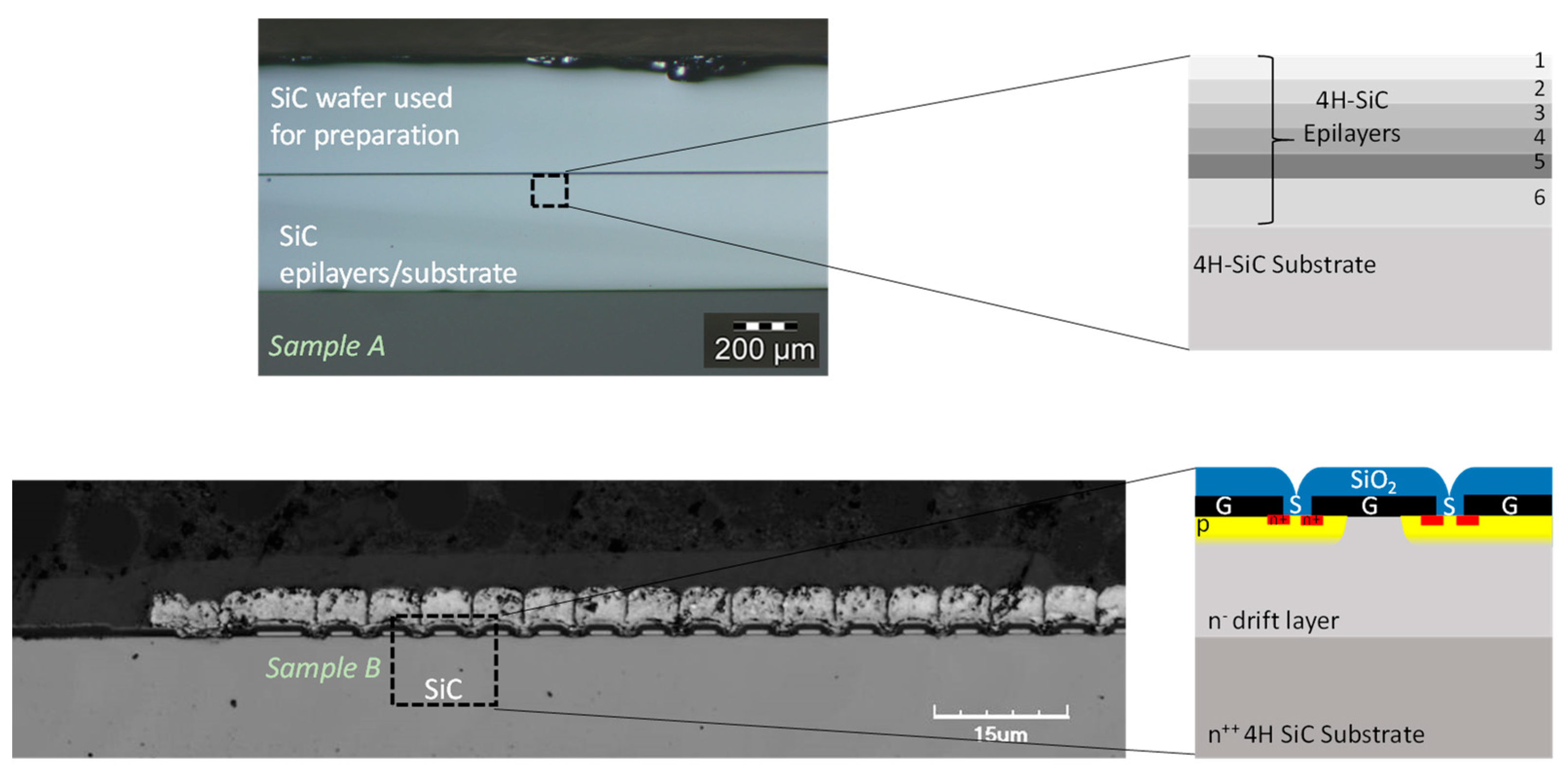
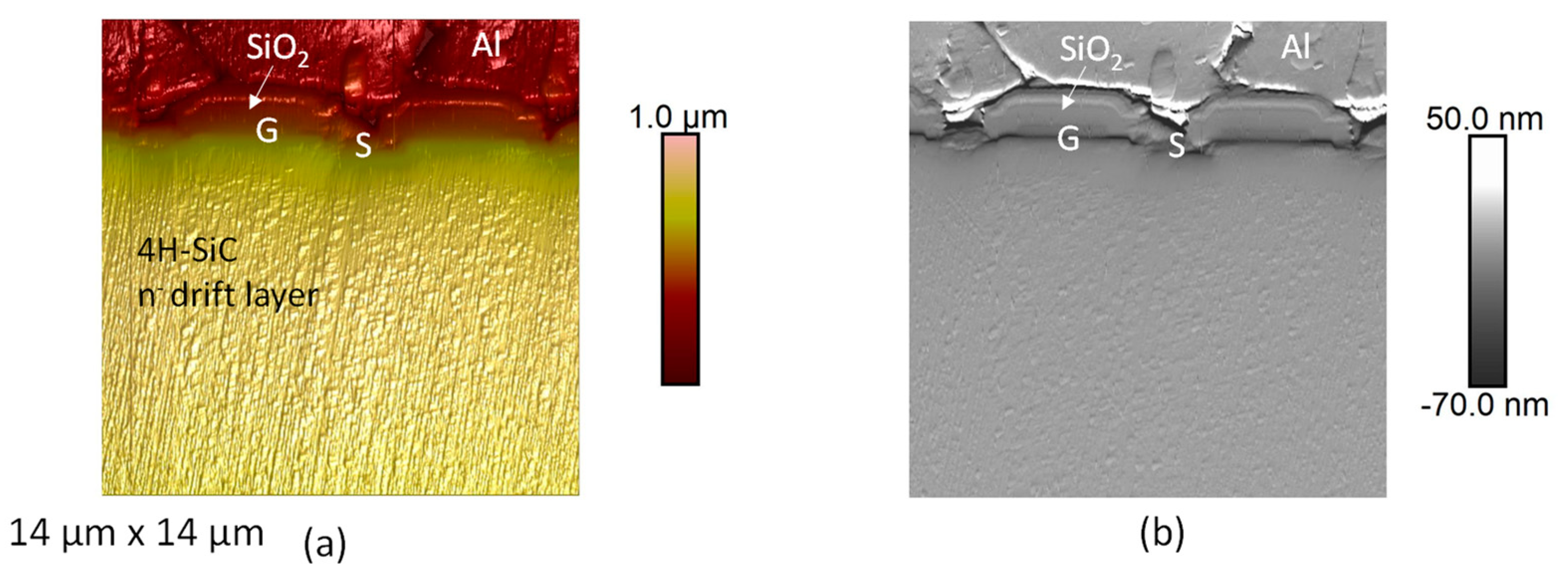
2.1. Description of the SiC Staircase Sample and MOSFET Device
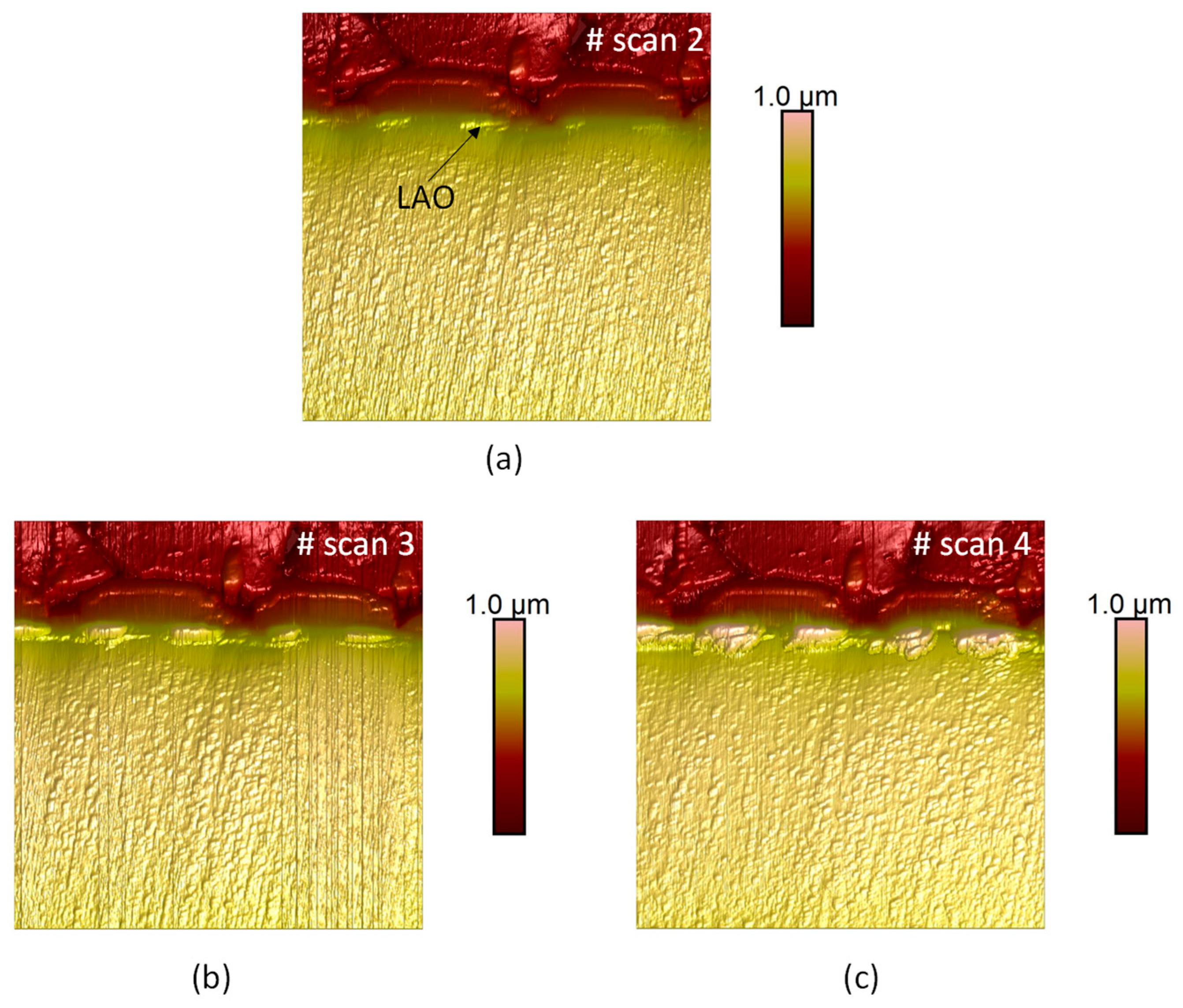
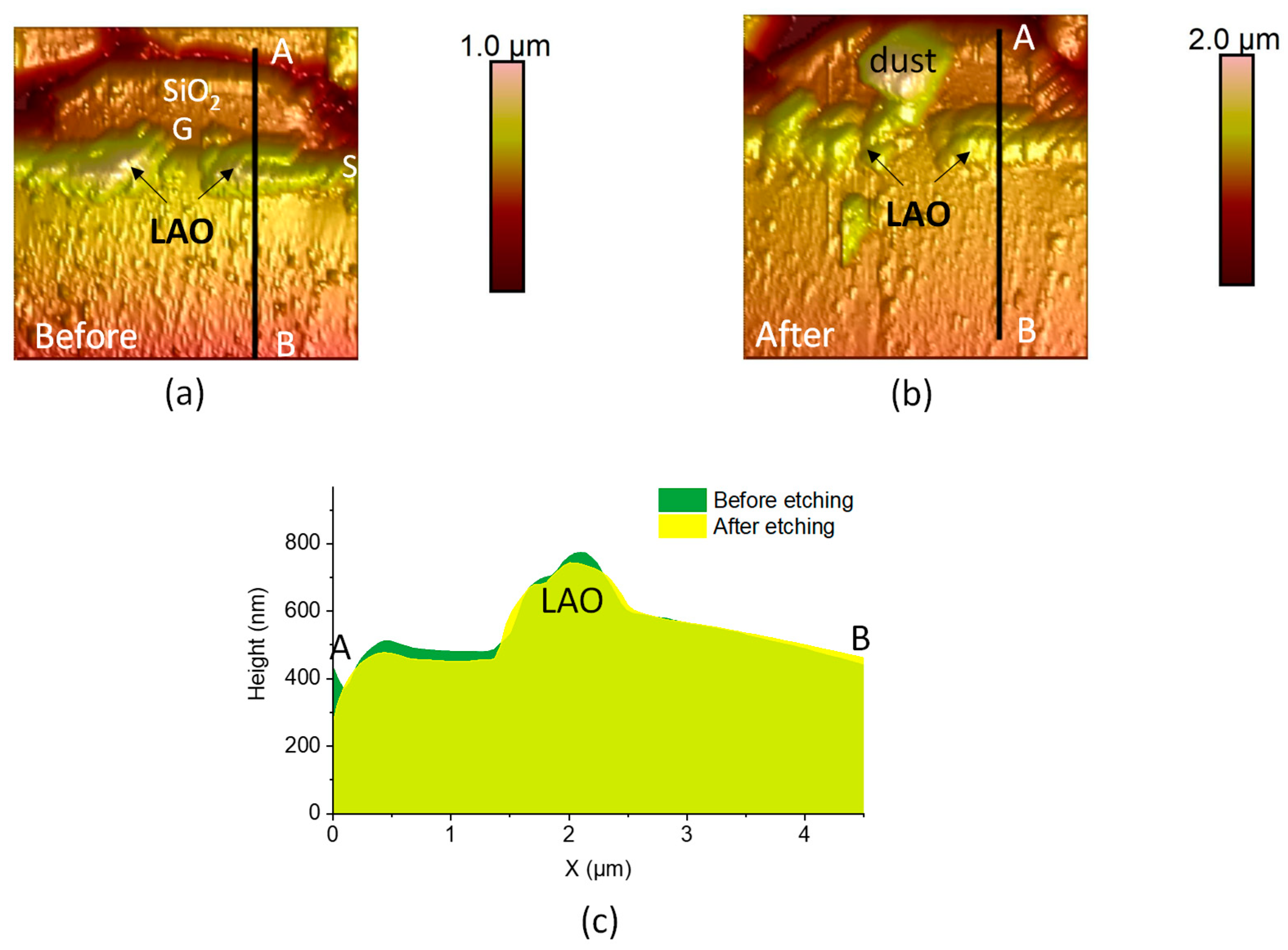
2.2. Atomic Force Measurement Details
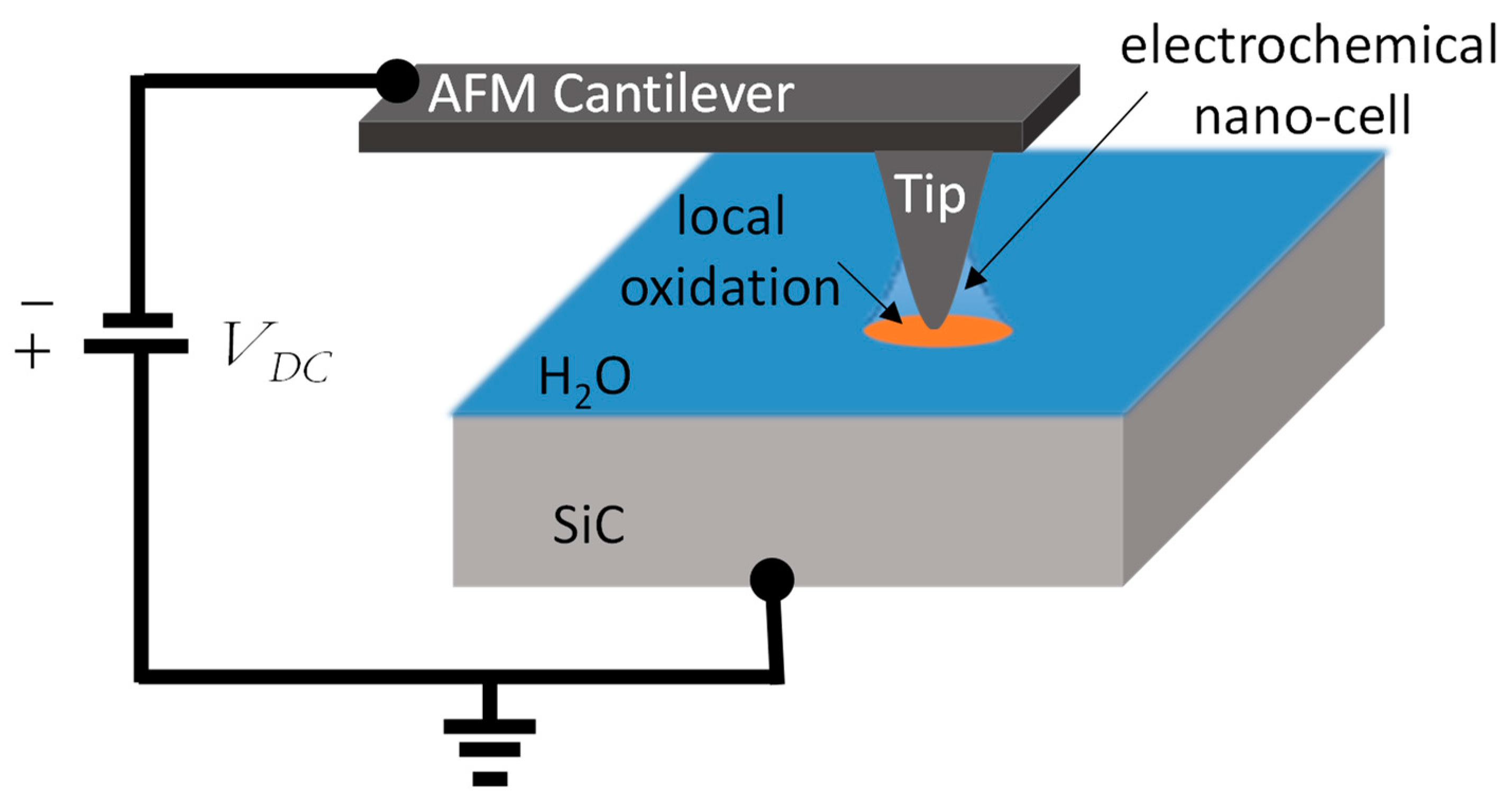
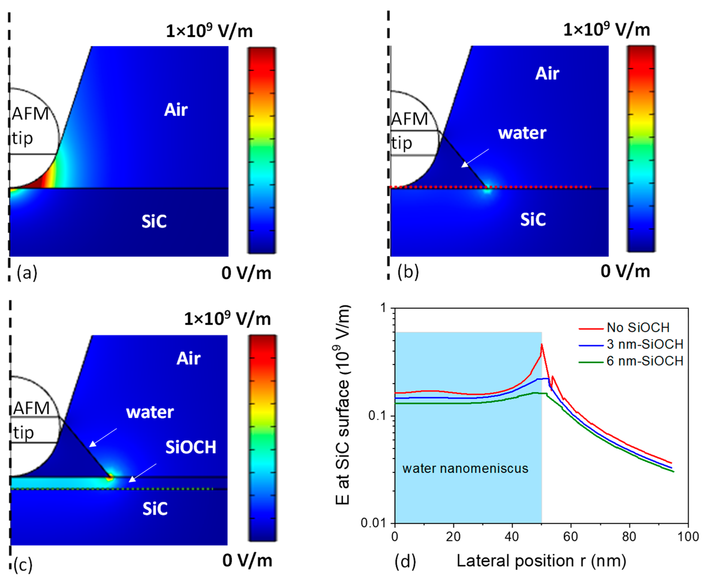
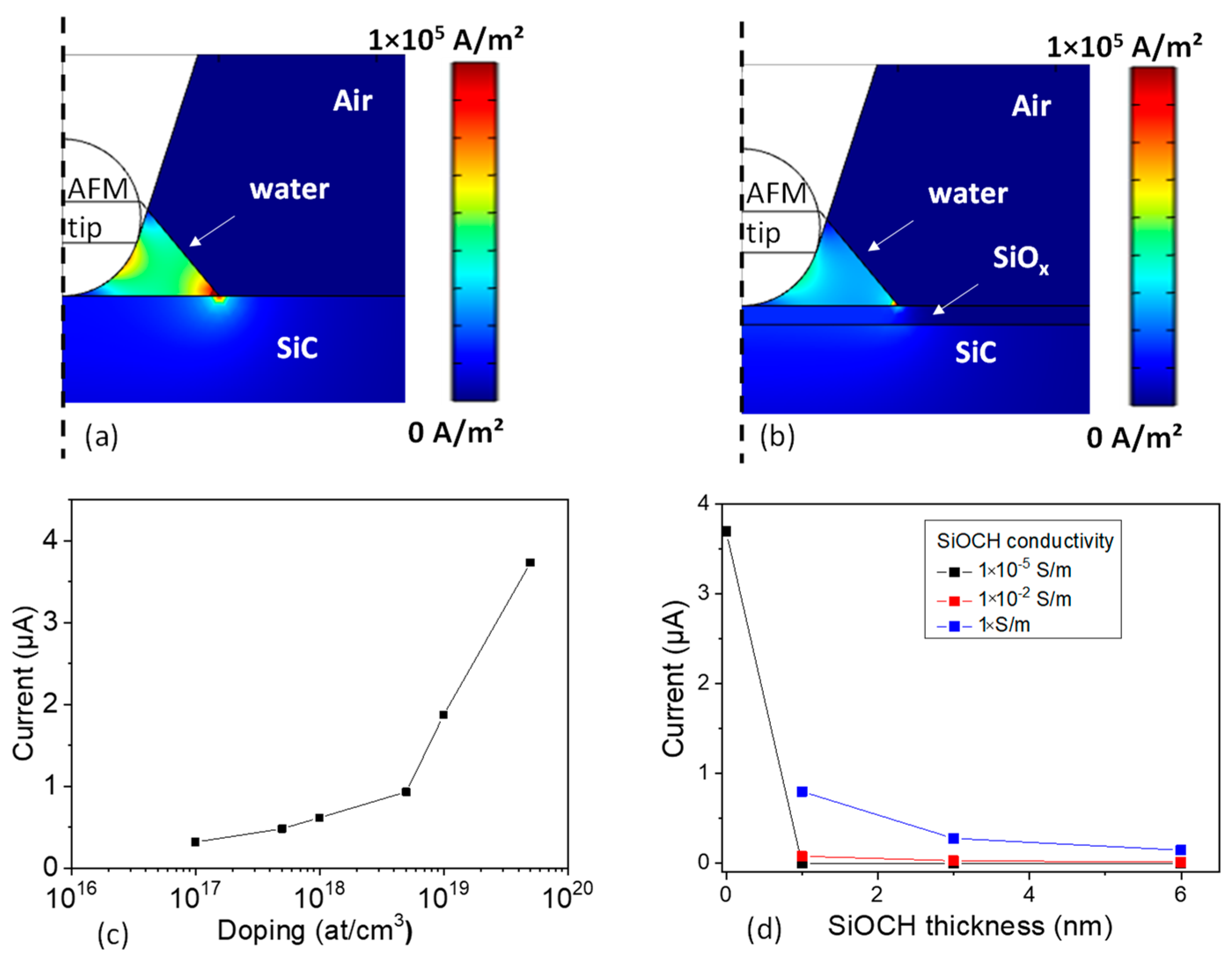
2.3. Simulations of the Electric Field and Current Distribution under the Tip–SiC Nanocontact
3. Results and Discussion
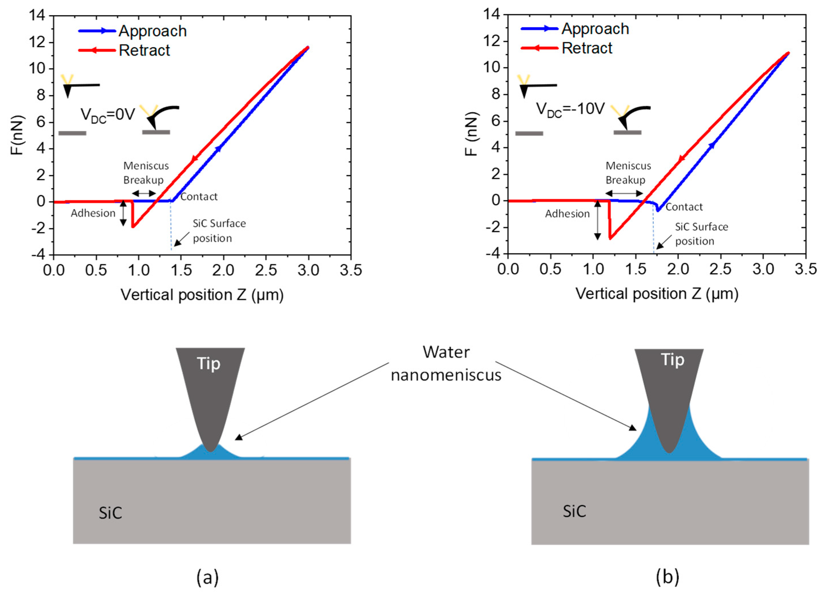
3.1. The Tip–Sample Interaction in Ambient Conditions: Signature of the Water Meniscus
3.2. Electrical Conduction at the Nanoscale
4. Results for the SiC-MOSFET
5. Conclusions
Author Contributions
Funding
Institutional Review Board Statement
Informed Consent Statement
Data Availability Statement
Acknowledgments
Conflicts of Interest
References
- Kumar, A.; Moradpour, M.; Losito, M.; Franke, W.-T.; Ramasamy, S.; Baccoli, R.; Gatto, G. Wide Band Gap Devices and Their Application in Power Electronics. Energies 2022, 15, 9172. [Google Scholar] [CrossRef]
- Neudeck, P.G.; Spry, D.J.; Chen, L.; Prokop, N.F.; Krasowski, M.J. Demonstration of 4H-SiC Digital Integrated Circuits Above 800 °C. IEEE Electron Device Lett. 2017, 38, 1082–1085. [Google Scholar] [CrossRef]
- Casady, J.; Johnson, R. Status of silicon carbide (SiC) as a wide-bandgap semiconductor for high-temperature applications: A review. Solid-State Electron. 1996, 39, 1409–1422. [Google Scholar] [CrossRef]
- Umegami, H.; Harada, T.; Nakahara, K. Performance Comparison of Si IGBT and SiC MOSFET Power Module Driving IPMSM or IM under WLTC. World Electr. Veh. J. 2023, 14, 112. [Google Scholar] [CrossRef]
- High-Voltage SiC Power Devices for Improved Energy Efficiency. Available online: https://www.jstage.jst.go.jp/article/pjab/98/4/98_PJA9804B-02/_article (accessed on 2 June 2023).
- Murray, H.; Germanicus, R.; Doukkali, A.; Martin, P.; Domenges, B.; Descamps, P. Analytic description of scanning capacitance microscopy. J. Vac. Sci. Technol. B Microelectron. Nanometer Struct. Process. Meas. Phenom. 2007, 25, 1340–1352. [Google Scholar] [CrossRef]
- Suda, J.; Nakamura, S.-I.; Miura, M.; Kimoto, T.; Matsunami, H. Scanning Capacitance and Spreading Resistance Microscopy of SiC Multiple-pn-Junction Structure. Jpn. J. Appl. Phys. 2002, 41, L40. [Google Scholar] [CrossRef]
- Cho, Y.C.Y.; Kazuta, S.K.S.; Ohara, K.O.K.; Odagawa, H.O.H. Quantitative Measurement of Linear and Nonlinear Dielectric Characteristics Using Scanning Nonlinear Dielectric Microscopy. Jpn. J. Appl. Phys. 2000, 39, 3086. [Google Scholar] [CrossRef]
- Chinone, N.; Cho, Y. Visualization of Gate-Bias-Induced Carrier Redistribution in SiC Power DIMOSFET Using Scanning Nonlinear Dielectric Microscopy. IEEE Trans. Electron Devices 2016, 63, 3165–3170. [Google Scholar] [CrossRef]
- Yamasue, K.; Cho, Y. Surface Potential Fluctuations of SiO2/SiC Interfaces Investigated by Local Capacitance-Voltage Profiling Based on Time-Resolved Scanning Nonlinear Dielectric Microscopy. Mater. Sci. Forum 2022, 1062, 335–340. [Google Scholar] [CrossRef]
- Giannazzo, F.; Shtepliuk, I.; Ivanov, I.G.; Iakimov, T.; Kakanakova-Georgieva, A.; Schilirò, E.; Fiorenza, P.; Yakimova, R. Probing the uniformity of hydrogen intercalation in quasi-free-standing epitaxial graphene on SiC by micro-Raman mapping and conductive atomic force microscopy. Nanotechnology 2019, 30, 284003. [Google Scholar] [CrossRef]
- Eriksson, J.; Roccaforte, F.; Giannazzo, F.; Nigro, R.L.; Raineri, V.; Lorenzzi, J.; Ferro, G. Improved Ni/3C-SiC contacts by effective contact area and conductivity increases at the nanoscale. Appl. Phys. Lett. 2009, 94, 112104. [Google Scholar] [CrossRef]
- Giannazzo, F.; Fiorenza, P.; Saggio, M.; Roccaforte, F. Nanoscale Characterization of SiC Interfaces and Devices. Mater. Sci. Forum 2014, 778–780, 407–413. [Google Scholar] [CrossRef]
- Fiorenza, P.; Schilirò, E.; Giannazzo, F.; Bongiorno, C.; Zielinski, M.; La Via, F.; Roccaforte, F. On the origin of the premature breakdown of thermal oxide on 3C-SiC probed by electrical scanning probe microscopy. Appl. Surf. Sci. 2020, 526, 146656. [Google Scholar] [CrossRef]
- Park, G.; Choi, Y.; Shin, S.; Lee, Y.; Hong, S. Nanoscale Visualization of the Electron Conduction Channel in the SiO/Graphite Composite Anode. ACS Appl. Mater. Interfaces 2022, 14, 30639–30648. [Google Scholar] [CrossRef]
- Elpelt, R.; Zippelius, B.; Doering, S.; Winkler, U. Employing Scanning Spreading Resistance Microscopy (SSRM) for Improving TCAD Simulation Accuracy of Silicon Carbide. Mater. Sci. Forum 2017, 897, 295–298. [Google Scholar] [CrossRef]
- Germanicus, R.C.; Leclère, P.; Guhel, Y.; Boudart, B.; Touboul, A.D.; Descamps, P.; Hug, E.; Eyben, P. On the effects of a pressure induced amorphous silicon layer on consecutive spreading resistance microscopy scans of doped silicon. J. Appl. Phys. 2015, 117, 244306. [Google Scholar] [CrossRef]
- Song, X.; Michaud, J.F.; Cayrel, F.; Zielinski, M.; Portail, M.; Chassagne, T.; Collard, E.; Alquier, D. Evidence of electrical activity of extended defects in 3C–SiC grown on Si. Appl. Phys. Lett. 2010, 96, 142104. [Google Scholar] [CrossRef]
- Chang, A.S.; Li, B.; Wang, S.; Frisone, S.; Goldman, R.S.; Han, J.; Lauhon, L.J. Unveiling the influence of selective-area-regrowth interfaces on local electronic properties of GaN p-n junctions for efficient power devices. Nano Energy 2022, 102, 107689. [Google Scholar] [CrossRef]
- Germanicus, R.C.; De Wolf, P.; Lallemand, F.; Bunel, C.; Bardy, S.; Murray, H.; Lüders, U. Mapping of integrated PIN diodes with a 3D architecture by scanning microwave impedance microscopy and dynamic spectroscopy. Beilstein J. Nanotechnol. 2020, 11, 1764–1775. [Google Scholar] [CrossRef]
- Millán-Barba, J.; Bakkali, H.; Lloret, F.; Gutiérrez, M.; de Villoria, R.G.; Domínguez, M.; Haenen, K.; Araujo, D. Boron-doped diamond growth on carbon fibre: Enhancing the electrical conductivity. Appl. Surf. Sci. 2023, 615, 156382. [Google Scholar] [CrossRef]
- Rius, G.; Lorenzoni, M.; Matsui, S.; Tanemura, M.; Perez-Murano, F. Boosting the local anodic oxidation of silicon through carbon nanofiber atomic force microscopy probes. Beilstein J. Nanotechnol. 2015, 6, 215–222. [Google Scholar] [CrossRef] [PubMed]
- Gordon, A.E.; Fayfield, R.T.; Litfin, D.D.; Higman, T.K. Mechanisms of surface anodization produced by scanning probe microscopes. J. Vac. Sci. Technol. B Microelectron. Nanometer Struct. Process. Meas. Phenom. 1995, 13, 2805–2808. [Google Scholar] [CrossRef]
- Ma, Y.-R.; Yu, C.; Yao, Y.-D.; Liou, Y.; Lee, S.-F. Tip-induced local anodic oxidation on the native SiO2 layer of Si(111) using an atomic force microscope. Phys. Rev. B 2001, 64, 195324. [Google Scholar] [CrossRef]
- Jo, Y.-D.; Seo, S.-H.; Bahng, W.; Kim, S.-C.; Kim, N.-K.; Koo, S.-M. Improved local oxidation of silicon carbide using atomic force microscopy. Appl. Phys. Lett. 2010, 96, 082105. [Google Scholar] [CrossRef]
- Gao, J.; Luo, X.; Chang, W.; Qin, Y.; Xie, W.; Fan, P.; Hasan, R.M.M.; Geng, Y.; Yan, Y. Three-Dimensional Nanostructures Enabled by Customised Voltage Waveform-Induced Local Anodic Oxidation Lithography. In Proceedings of the 22nd EUSPEN International Conference and Exhibition, Geneva, Switzerland, 30 May–3 June 2022; pp. 285–288. [Google Scholar]
- Ryu, Y.K.; Knoll, A.W. Oxidation and Thermal Scanning Probe Lithography for High-Resolution Nanopatterning and Nanodevices. Electrical Atomic Force Microscopy for Nanoelectronics. In NanoScience and Technology; Celano, U., Ed.; Springer International Publishing: Cham, Switzerland, 2019; pp. 143–172. [Google Scholar] [CrossRef]
- Colangelo, F.; Piazza, V.; Coletti, C.; Roddaro, S.; Beltram, F.; Pingue, P. Local anodic oxidation on hydrogen-intercalated graphene layers: Oxide composition analysis and role of the silicon carbide substrate. Nanotechnology 2017, 28, 105709. [Google Scholar] [CrossRef]
- Xie, X.N.; Chung, H.J.; Sow, C.H.; Wee, A.T.S. Native oxide decomposition and local oxidation of 6H-SiC (0001) surface by atomic force microscopy. Appl. Phys. Lett. 2004, 84, 4914–4916. [Google Scholar] [CrossRef]
- Lorenzoni, M.; Torre, B. Scanning probe oxidation of SiC, fabrication possibilities and kinetics considerations. Appl. Phys. Lett. 2013, 103, 163109. [Google Scholar] [CrossRef]
- Lee, J.H.; Ahn, J.J.; Hallén, A.; Zetterling, C.M.; Koo, S.M. Local Anodic Oxidation of Phosporous-Implanted 4H-SiC by Atomic Force Microscopy. Mater. Sci. Forum 2012, 717–720, 905–908. [Google Scholar] [CrossRef]
- Germanicus, R.C.; Jouha, W.; Moultif, N.; De Wolf, P.; Shah, V.A.; Gammon, P.M.; Luders, U.; Latry, O. Parametric nano-electrical analysis for SiC junctions of a packaged device. In Proceedings of the 2022 IEEE Workshop on Wide Bandgap Power Devices and Applications in Europe (WiPDA Europe), Coventry, UK, 18–20 September 2022; pp. 1–6. [Google Scholar] [CrossRef]
- Ryu, Y.K.; Garcia, R. Advanced oxidation scanning probe lithography. Nanotechnology 2017, 28, 142003. [Google Scholar] [CrossRef]
- Liu, H.; Hoeppener, S.; Schubert, U.S. Nanoscale Materials Patterning by Local Electrochemical Lithography. Adv. Eng. Mater. 2016, 18, 890–902. [Google Scholar] [CrossRef]
- Villeneuve-Faure, C.; Makasheva, K.; Boudou, L.; Teyssedre, G. Charge injection in thin dielectric layers by atomic force microscopy: Influence of geometry and material work function of the AFM tip on the injection process. Nanotechnology 2016, 27, 245702. [Google Scholar] [CrossRef]
- Xi, J.; Liu, C.; Morgan, D.; Szlufarska, I. An Unexpected Role of H During SiC Corrosion in Water. J. Phys. Chem. C 2020, 124, 9394–9400. [Google Scholar] [CrossRef]
- HButt, H.-J.; Cappella, B.; Kappl, M. Force measurements with the atomic force microscope: Technique, interpretation and applications. Surf. Sci. Rep. 2005, 59, 1–152. [Google Scholar] [CrossRef]
- Cappella, B.; Dietler, G. Force-distance curves by atomic force microscopy. Surf. Sci. Rep. 1999, 34, 1–104. [Google Scholar] [CrossRef]
- Rozhok, S.; Sun, P.; Piner, R.; Lieberman, M.; Mirkin, C.A. AFM Study of Water Meniscus Formation between an AFM Tip and NaCl Substrate. J. Phys. Chem. B 2004, 108, 7814–7819. [Google Scholar] [CrossRef]
- Bartošík, M.; Kormoš, L.; Flajšman, L.; Kalousek, R.; Mach, J.; Lišková, Z.; Nezval, D.; Švarc, V.; Šamořil, T.; Šikola, T. Nanometer-Sized Water Bridge and Pull-Off Force in AFM at Different Relative Humidities: Reproducibility Measurement and Model Based on Surface Tension Change. J. Phys. Chem. B 2017, 121, 610–619. [Google Scholar] [CrossRef]
- Sirghi, L.; Szoszkiewicz, R.; Riedo, E. Volume of a Nanoscale Water Bridge. Langmuir 2006, 22, 1093–1098. [Google Scholar] [CrossRef]
- Cabrera, N.; Mott, N.F. Theory of the oxidation of metals. Rep. Prog. Phys. 1949, 12, 163. [Google Scholar] [CrossRef]
- NNasir, N.M.; Shah, C.; Leech, P.; Reeves, G.; Pirogova, E.; Istivan, T.; Tanner, P.; Holland, A. Fabrication of 3C-silicon carbide membranes: Towards development of novel microdevices for biomedical applications. In Proceedings of the 2012 International Conference on Biomedical Engineering (ICoBE), Penang, Malaysia, 27–28 February 2012; pp. 589–593. [Google Scholar] [CrossRef]


Disclaimer/Publisher’s Note: The statements, opinions and data contained in all publications are solely those of the individual author(s) and contributor(s) and not of MDPI and/or the editor(s). MDPI and/or the editor(s) disclaim responsibility for any injury to people or property resulting from any ideas, methods, instructions or products referred to in the content. |
© 2023 by the authors. Licensee MDPI, Basel, Switzerland. This article is an open access article distributed under the terms and conditions of the Creative Commons Attribution (CC BY) license (https://creativecommons.org/licenses/by/4.0/).
Share and Cite
Villeneuve-Faure, C.; Boumaarouf, A.; Shah, V.; Gammon, P.M.; Lüders, U.; Coq Germanicus, R. SiC Doping Impact during Conducting AFM under Ambient Atmosphere. Materials 2023, 16, 5401. https://doi.org/10.3390/ma16155401
Villeneuve-Faure C, Boumaarouf A, Shah V, Gammon PM, Lüders U, Coq Germanicus R. SiC Doping Impact during Conducting AFM under Ambient Atmosphere. Materials. 2023; 16(15):5401. https://doi.org/10.3390/ma16155401
Chicago/Turabian StyleVilleneuve-Faure, Christina, Abdelhaq Boumaarouf, Vishal Shah, Peter M. Gammon, Ulrike Lüders, and Rosine Coq Germanicus. 2023. "SiC Doping Impact during Conducting AFM under Ambient Atmosphere" Materials 16, no. 15: 5401. https://doi.org/10.3390/ma16155401
APA StyleVilleneuve-Faure, C., Boumaarouf, A., Shah, V., Gammon, P. M., Lüders, U., & Coq Germanicus, R. (2023). SiC Doping Impact during Conducting AFM under Ambient Atmosphere. Materials, 16(15), 5401. https://doi.org/10.3390/ma16155401