Article

Adoption of the Wet Surface Treatment Technique for the Improvement of Device Performance of Enhancement-Mode AlGaN/GaN MOSHEMTs for Millimeter-Wave Applications

1
Department of Material Science Engineering, National Yang Ming Chiao Tung University, 1001 Tah Hsueh Road, Hsinchu 30010, Taiwan
2
Department of Electrical Engineering, National Yang Ming Chiao Tung University, 1001 Tah Hsueh Road, Hsinchu 30010, Taiwan
3
International College of Semiconductor Technology, National Yang Ming Chiao Tung University, 1001 Tah Hsueh Road, Hsinchu 30010, Taiwan
4
Institute of Microengineering and Nanoelectronics (IMEN) Level 4, Research Complex, University Kebangsaan Malaysia, Bangi 43600, Malaysia
*
Author to whom correspondence should be addressed.
Materials 2021, 14(21), 6558; https://doi.org/10.3390/ma14216558
Submission received: 2 October 2021 / Revised: 23 October 2021 / Accepted: 28 October 2021 / Published: 1 November 2021
(This article belongs to the Special Issue Advances in III-V Integration Materials and Devices)

Abstract

:
In this work, a low-power plasma oxidation surface treatment followed by Al2O3 gate dielectric deposition technique is adopted to improve device performance of the enhancement-mode (E-mode) AlGaN/GaN metal-oxide-semiconductor high-electron-mobility transistors (MOSHEMTs) intended for applications at millimeter-wave frequencies. The fabricated device exhibited a threshold voltage (Vth) of 0.13 V and a maximum transconductance (gm) of 484 (mS/mm). At 38 GHz, an output power density of 3.22 W/mm with a power-added efficiency (PAE) of 34.83% were achieved. Such superior performance was mainly attributed to the high-quality Al2O3 layer with a smooth surface which also suppressed the current collapse phenomenon.

1. Introduction

The quest for a high-capacity 5G network for increased data transmission requires wide bandwidth and high signal-to-noise ratio (SNR) to maintain the quality of service (QoS) of the system. Since the spectrum below 20 GHz has been crowded with commercial applications, allocation of bandwidth wide enough to accommodate the required channel capacity is almost impossible. As a result, operating at millimeter-wave frequencies has been the only solution for next-generation communication systems targeting at multi-giga-bit data transmission with minimum latency. In comparison with Si- and GaAs-based transistors, GaN-based HEMTs exhibit superior performance at high frequencies in terms of power density and efficiency due to the characteristics of the wide bandgap, high electron mobility and large breakdown field of GaN material. Successful demonstrations of the depletion-mode (D-mode) devices have been reported in [1,2,3].
Other than the D-mode devices, the E-mode devices exhibit certain advantages in terms of practical operations at system level. Since the devices require only positive supply, the complexity of the biasing network can greatly be reduced. Moreover, elimination of the negative supply also helps the suppression of the system noise. In the past, several approaches were reported for the development of E-mode devices. Fluorine plasma treatment was applied to insert negative charges into the barrier layer, resulting in a positive shift with the threshold voltage as a depletion region was formed in the 2DEG channel. A maximum output power density of 3.6 W/mm and peak PAE of 42% were measured at 18 GHz from the E-mode AlGaN/GaN heterojunction FET (HFET) [4]. However, the current collapse is a big issue caused by the plasma implantation. The technique of applying a p-type GaN layer under the gate region can help avoiding the damage caused by plasma. Normally-off HEMTs with the formation of the p-n junction exhibited the cut-off frequency (fT) and maximum oscillation frequency (fmax) of 6.0 and 9.8 GHz by adopting a gate-all-around structure in [5].
Gate recess is the major technology for the realization of the E-mode devices [6,7,8]. The barrier thickness under 8 nm with a proper gate-recessed process exhibited excellent RF characteristics in terms of the fT and fmax in [8]. The major issue with a gate recess process is the unavoidable damage to the surface leading to possible performance degradations. Thus, techniques of surface treatment, damage-free gate recess, and dielectric passivation have been proposed to suppress the possible damage that causes the current collapse phenomenon [9,10,11,12,13,14,15]. There are various surface treatments and cleaning methods, such as UV/ozone [16], wet chemical [17], plasma [18], descum [19] and O2 treatment [20] which have been adopted for the improvement of the surface states. For instance, with the SF6 plasma treatment, the gate leakage and pulse I–V characteristics were improved effectively due to the reduction in the amount of carbon on the semiconductor surface [18]. Besides, an Al2O3 dielectric layer under the gate region was adopted to suppress the hydrogen-induced weak bonds for leakage current reduction in [11]. The fabricated E-mode metal-insulator-semiconductor HEMTs (MISHEMTs) demonstrated an output power density of 5.76 W/mm and a PAE of 57% at 4 GHz.
In this work, we fabricated an enhancement-mode AlGaN/GaN metal-oxide-semiconductor high-electron-mobility transistor (MOSHEMT) using the wet surface treatment technology followed by the deposition of a high-quality Al2O3 layer. Compared with hydrochloric acid cleaning, a better surface morphology was achieved after the adoption of the wet surface treatment. Moreover, the imperfect layer of the gate region surface which included the native oxide and the bombardment damage caused by the plasma etching process could be effectively removed. Improvement in the device performance was observed with such surface treatment due to the suppression of the current collapse phenomenon. The maximum output power density and peak PAE were measured to be 3.22 W/mm and 34.83%, respectively, at 38 GHz.

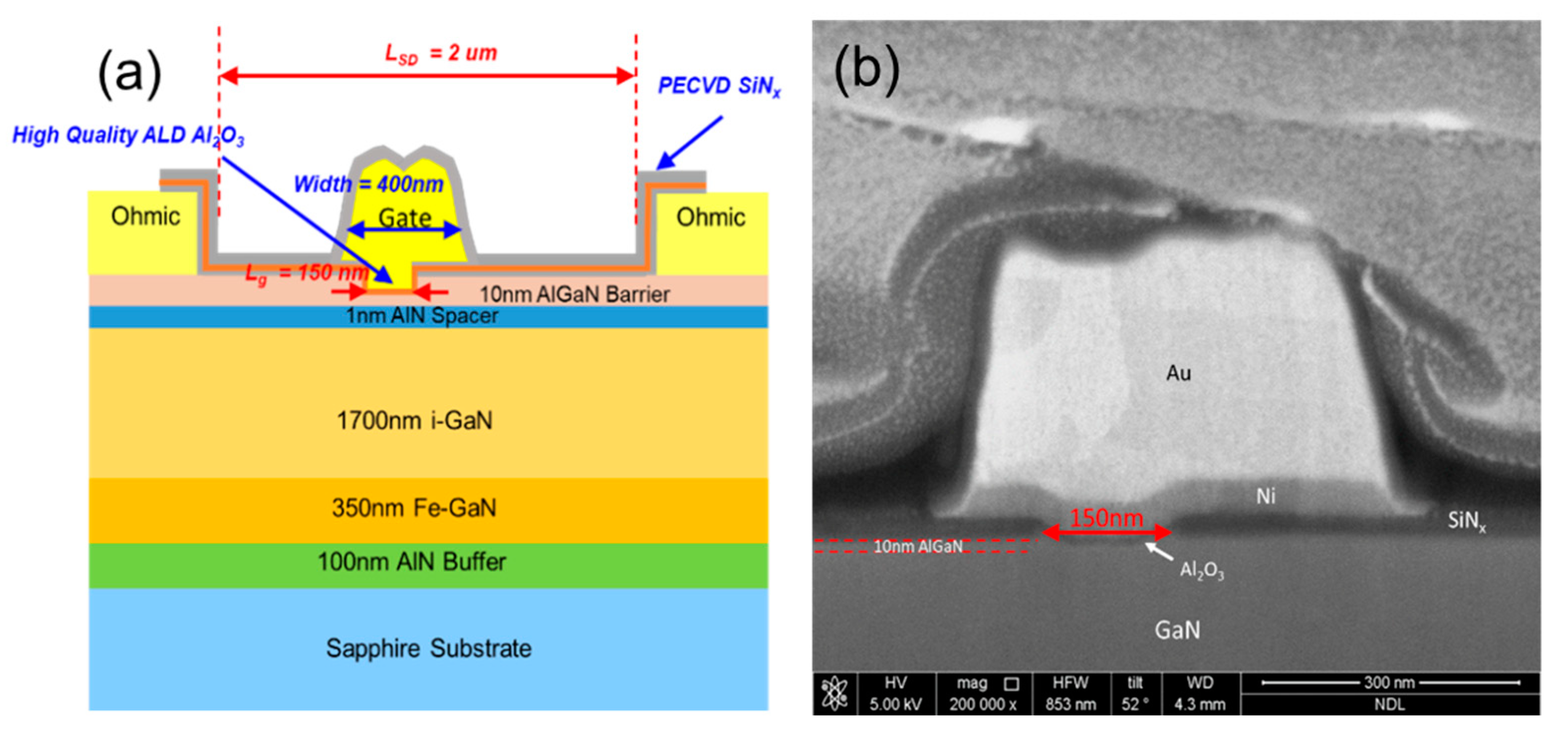
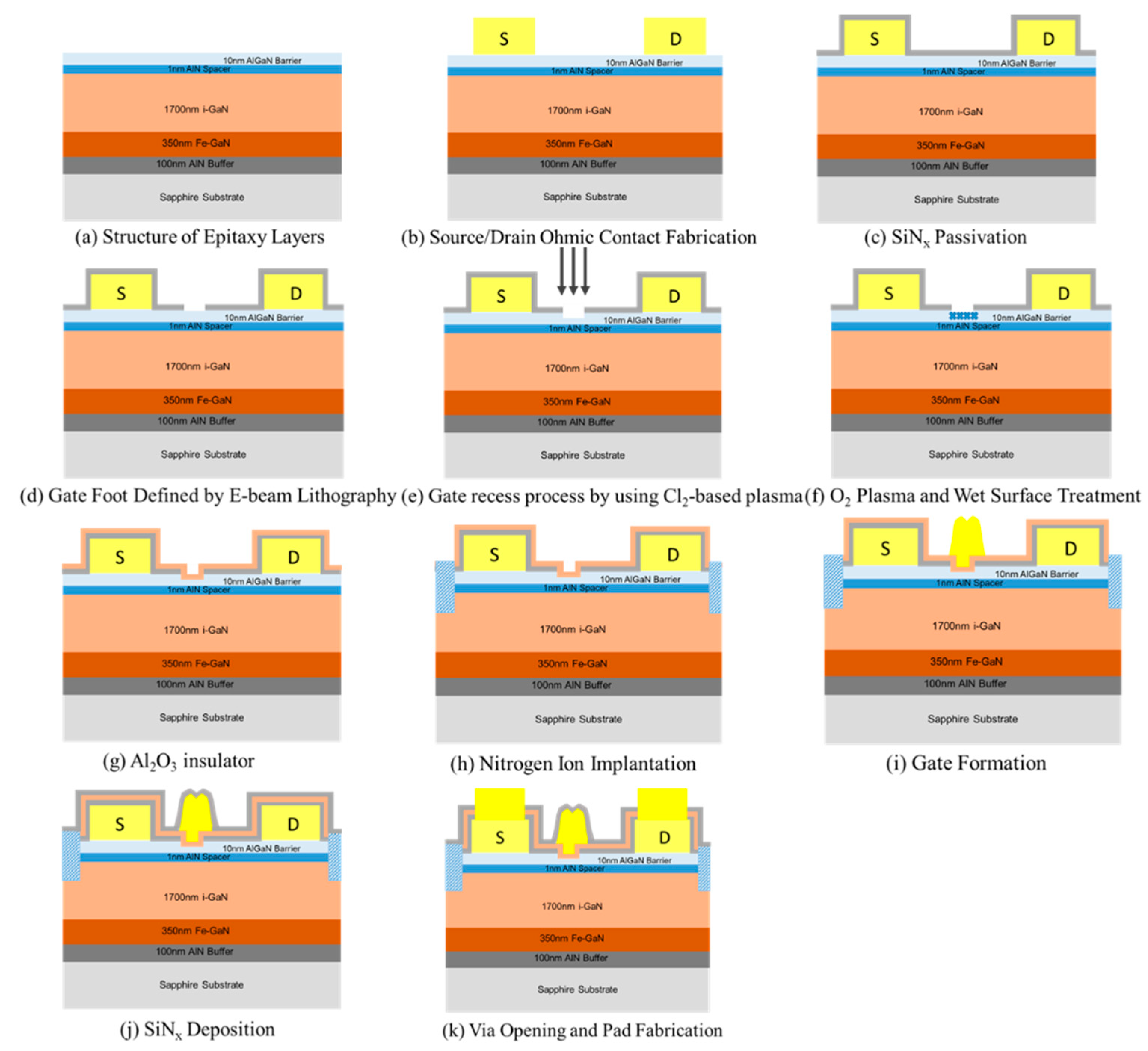
2. Materials and Methods

Figure 1 shows the cross section of the thin-barrier AlGaN/GaN MOSHEMT grown on 4-inch Sapphire substrate by metal-organic chemical vapor deposition. The T-gate with asymmetric head toward the drain side was adopted for the purpose of the breakdown-voltage enhancement. Figure 2 displays the top view SEM images of AlGaN/GaN MOSHEMTs at different magnifications. The epitaxial structure consists of a 100 nm AlN nucleation layer, a 350 nm iron-doped GaN buffer layer, a 1700 nm i-GaN layer, a 1 nm AlN spacer layer, and a 10 nm Al0.26Ga0.74N barrier layer. Room temperature Hall effect measurement exhibits a sheet carrier density of 9.7 × 1012 cm−2, a sheet resistance of 324 Ω/□, and an electron mobility of 1980 cm2/V·s, respectively. Figure 3 shows EDX analysis of aluminum and gallium elements. It is observed that the aluminum was rich in the AlGaN barrier and gradually decreased when it reached the GaN buffer layer. The cross-section HRTEM image is also shown in Figure 4.
Device fabrication started with the wafer cleaning by dipping in the acetone and isopropanol solution to remove the organic particles or contaminations. The ohmic contact consisted of a Ti/Al/Ni/Au metal stack deposited by ULVAC EVA650 E-gun evaporation system (EVA650, Ulvac, Hsinchu, Taiwan). Ohmic metal alloying was then formed at 820 °C for 30 s in N2 ambient using a Premtek RTP-T41 rapid thermal annealing (RTA) system. A 25 nm-SiNx was deposited by STS310PC plasma-enhanced chemical vapor deposition (PECVD) with in-situ nitrogen plasma treatment prior to the film deposition [21]. The SiNx film could reduce the dangling bond on the surface and act as hard mask at the recess region. The 150 nm gate foot was defined by using a 50 kV JEOL e-beam lithography (EBL) system (JBX 6000 FS) and the gate region was opened by fluorine-based ICP dry etching to remove SiNx film. Next, the gate recess process was performed using Cl2-based plasma with the following parameters: 40 sccm flow rate, 0.1 Pa pressure, and 200 W of RF power with 5 W of bottom bias. O2 plasma was performed by the ICP system (Nesca-20 plus, Cello Technology, Hsinchu, Taiwan) with low RF power of 50 W and the 5 W for the bottom bias. Afterwards, a thin oxide layer was formed on the surface. Then, the oxide layer was removed by wet surface treatment using NH4OH solution for 5 min. A 7 nm Al2O3 insulator was deposited by a Fujitec G2 atomic layer deposition (ALD) system (Fujitec G2, Veeco, Plainview, NYC, USA) immediately after the surface treatment. The growth rate was 1 Å/cycle for 70 cycles and the temperature was kept at 250 °C. Afterwards, the active region was defined by nitrogen ion implantation. With the use of the ZEP/GL-2000 photoresists, the T-shape gate was formed as shown in Figure 1 and the width of the foot and head were 150 nm and 400 nm. A 15 nm SiNx layer was deposited by PECVD after Ni/Au gate metal deposition and the lift-off process. The recessed depth of the gate region was approximately 4 nm. Finally, Ti/Au was deposited as an interconnect metal. The process flow is shown in Figure 5. The gate-source and gate-drain distance were 0.7 μm, and 1.1 μm, respectively.
Figure 6 shows the root mean square roughness of the AlGaN layer surface morphology by an atomic force microscope. Substantial reduction in the surface roughness from 0.66 nm to 0.4 nm was observed for the device with surface treatment. Moreover, an AFM image with an atomically clean morphology was achieved after applying the treatment.

3. Results and Discussion

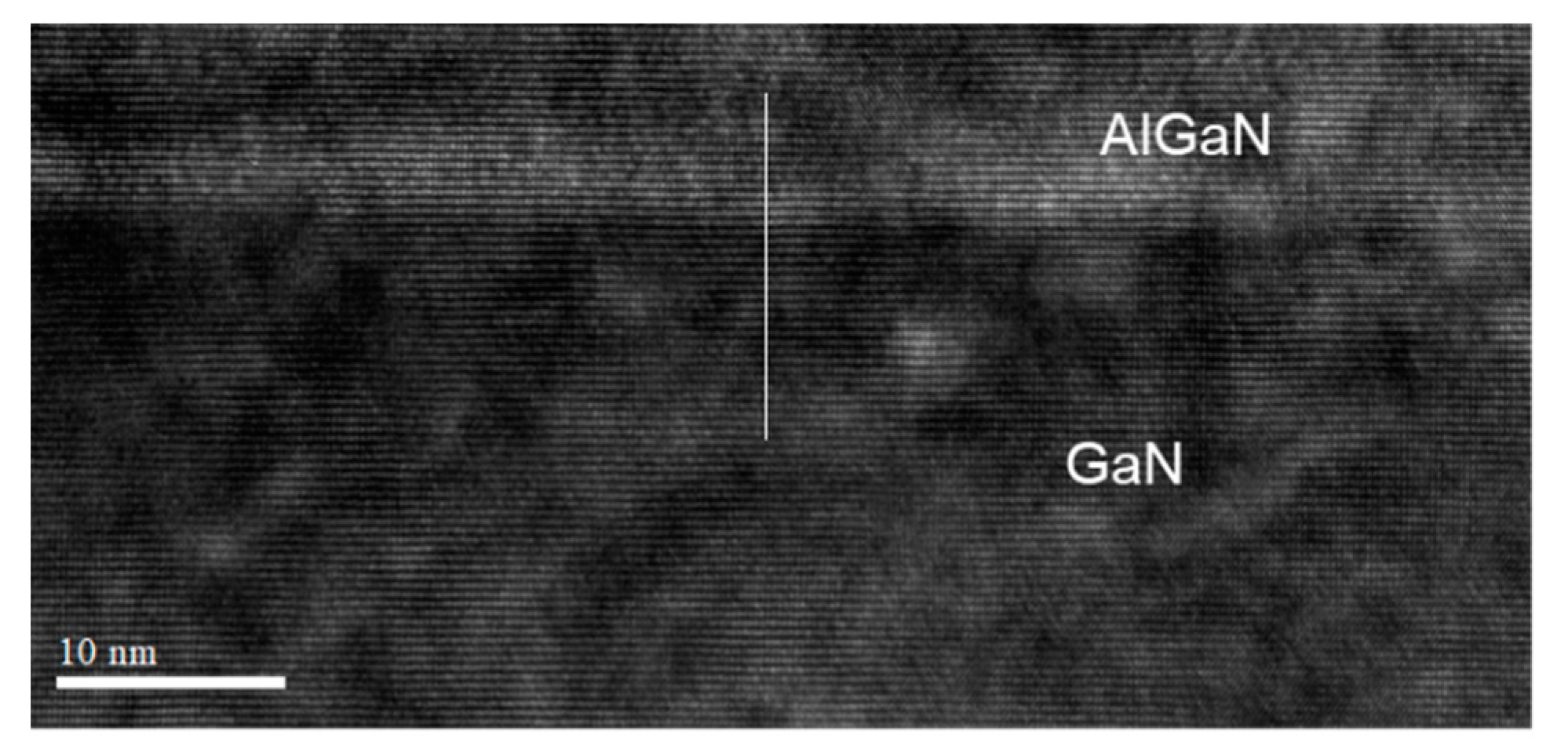
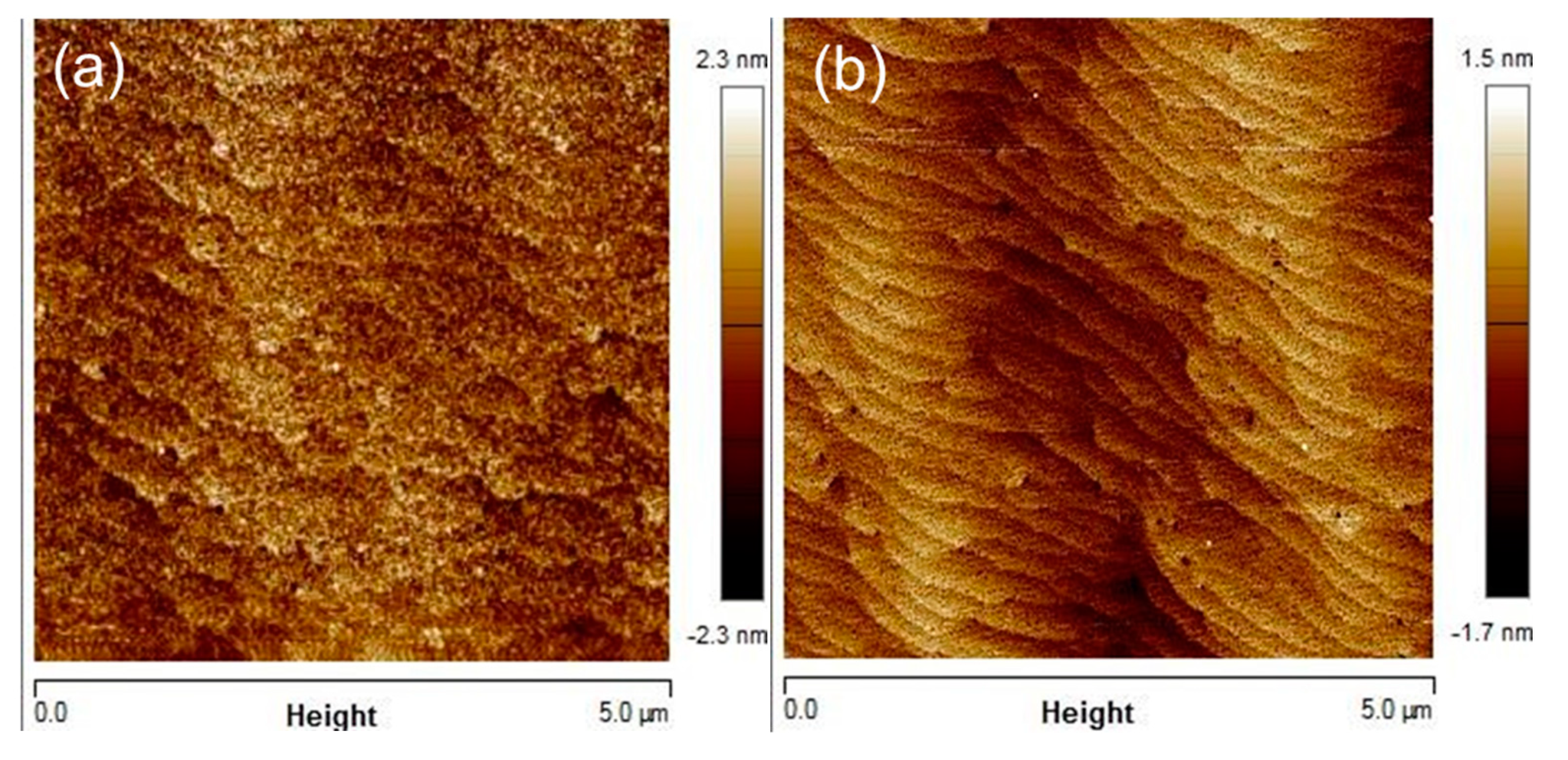
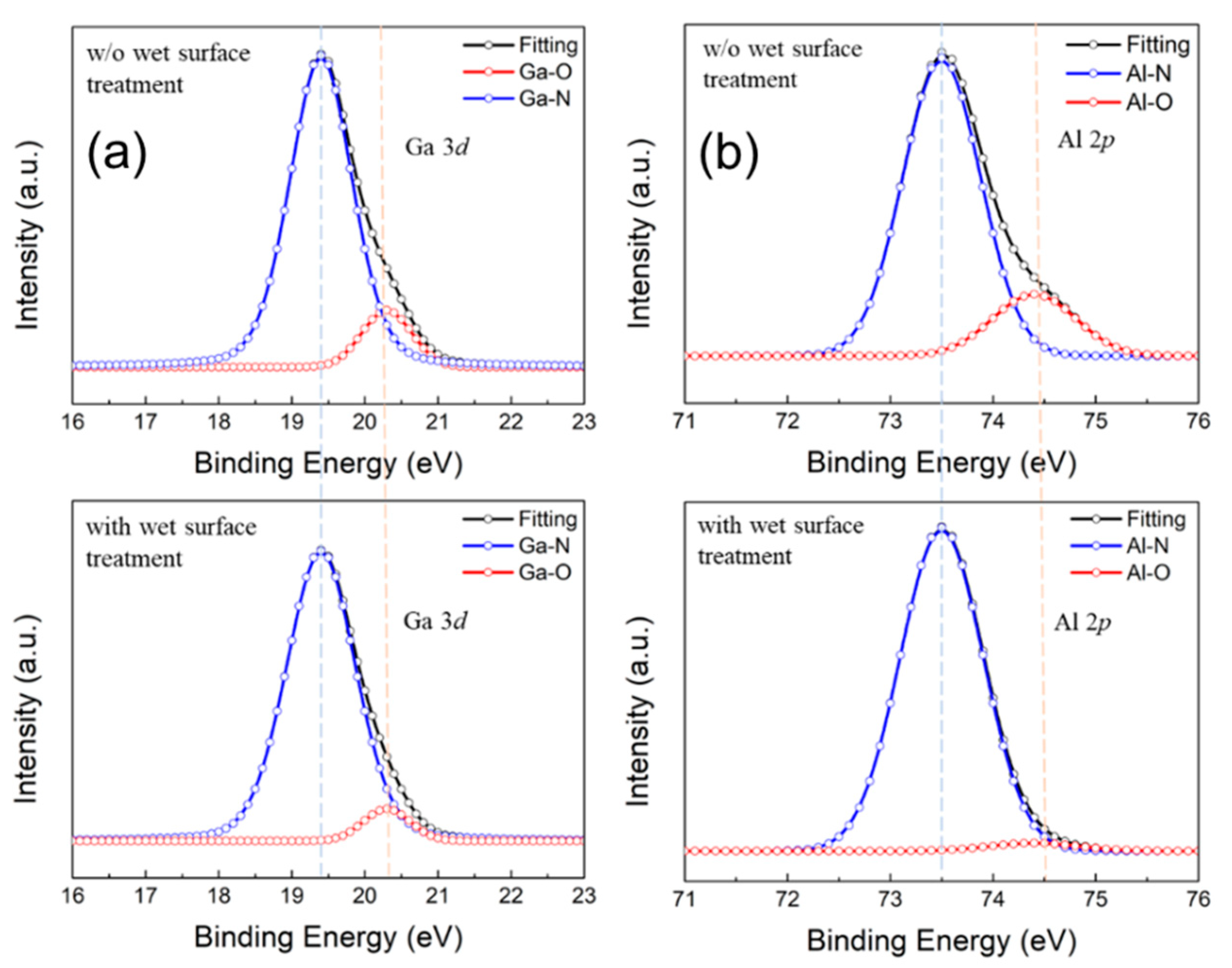
3.1. X-ray Photoelectron Spectroscopy (XPS) Measurement

X-ray photoelectron spectroscopy (XPS) was adopted to investigate the surface chemical composition after applying the wet surface treatment. Generally, an imperfect layer caused by the environment pollutants, the native oxide, and the bombardment damage existed after the gate recess process. The existence of such a layer would degrade the device characteristics. It is thus of crucial importance to address this issue especially for devices at millimeter-wave frequencies. Figure 7 shows the Ga 3d and Al 2p core-level spectra of the control sample with HCl surface treatment and the sample with wet surface treatment, respectively. The Ga 3d and Al 2p peaks were separated into four main peaks Ga–O, Ga–N, Al–O and Al–N bonds. It is obvious that the intensity of the Ga–O and Al–O with a larger binding energy are much lower in the experimental sample. In other words, the Ga–O and Al–O bonding proportion decreased at the surface region. Such an effect indicates that with the application of wet surface treatment, the imperfect layer can be effectively removed. In [17], the XPS analysis showed the reduction of the Ga–O and Al–O percentage after the TMAH treatment, which was considered to be the removal of the damage and the oxides at the AlGaN gate surface region.

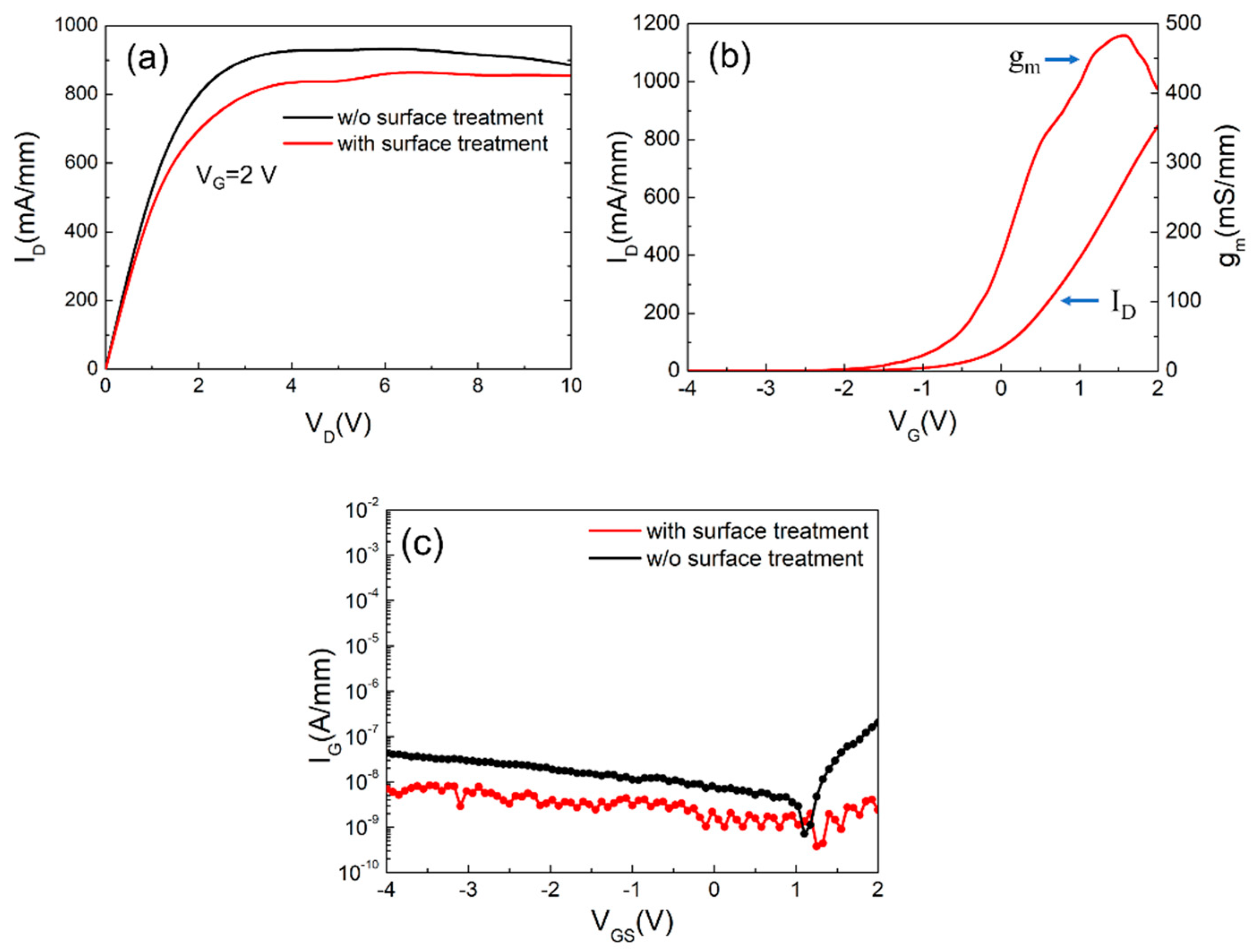
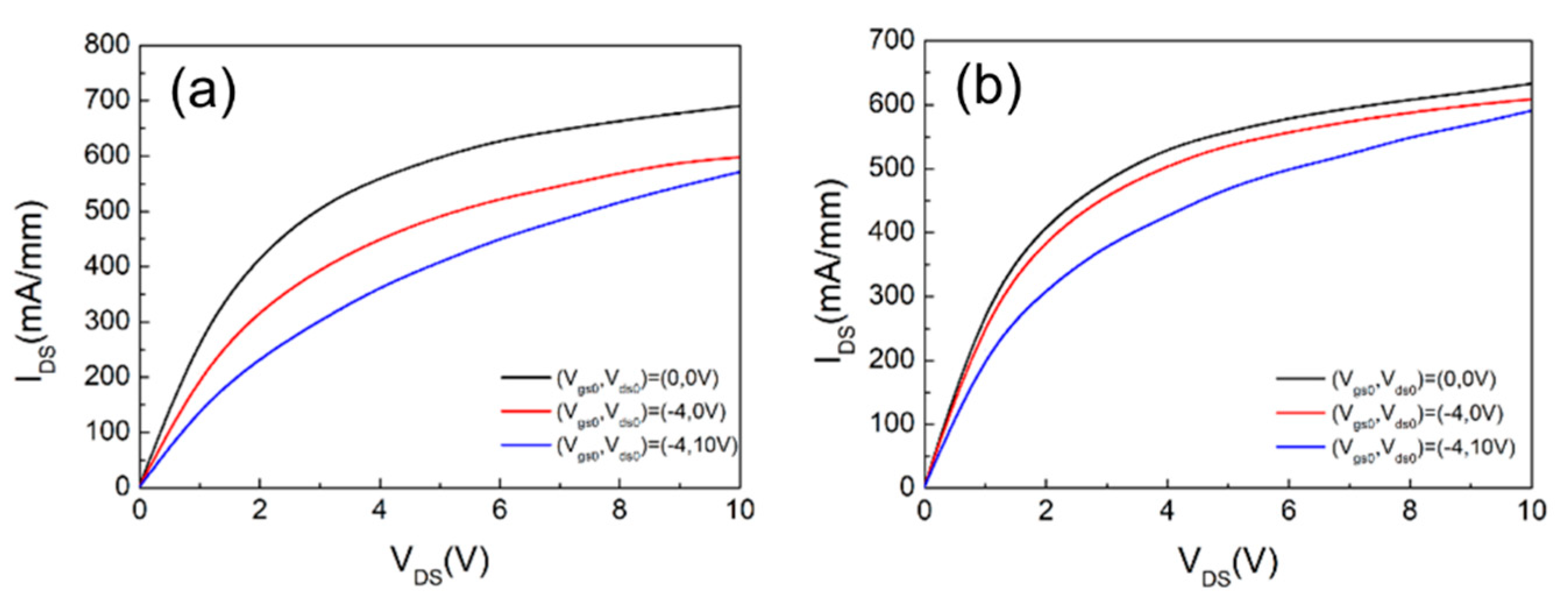
3.2. Direct Current (DC) and Pulsed Current–Voltage (I–V) Characteristics

The measured DC characteristics of the thin barrier E-mode AlGaN/GaN HEMTs is shown in Figure 8. As observed, the fabricated 2 × (0.15 × 25) μm2 devices with surface treatment exhibits a lower maximum drain current of 859 mA/mm compared to the devices without surface treatment, which has a maximum current of 931 mA/mm at VG = 2 V. After the wet surface treatment, a peak extrinsic transconductance (gm) 484 mS/mm and a threshold voltage (Vth) of +0.13 V were achieved at VDS = 5 V due to the removal of the surface oxidation layer by wet recess. While scaling down the distance between gate and channel, higher gm and lower current density were obtained for E-mode device. As for the gate leakage current for both cases shown in Figure 8c, further improvement in the leakage current is also observed for the device with surface treatment. The forward gate current of the device with wet surface treatment exhibited two orders of magnitude lower than that without surface treatment, evidencing the effect of the removal of the imperfect layer. Further investigation on the trapping levels at the interface was conducted through the pulsed-IV measurements. Figure 9 shows the results with a 200 ns pulse width and 0.1% duty cycle. With the gate stress measurements under a quiescent bias of (VGS0, VDS0) = (−4 V, 0 V), the device with wet surface treatment shows minor collapse ratio of 3.7% which is much smaller than that of 17.78% for the one without treatment. It is obvious that the plasma damage caused by the dry etching process can be suppressed after the combination of the oxidation and wet etching treatment. The drain lag ratio has also decreased from 17% to 12.58% at VGS = 1 V and VDS = 5 V under the condition (VGS0, VDS0) = (−4 V, 10 V). Improvement in the current collapse phenomenon has been identified from both drain and gate lad measurements. It is worth mentioning that the drain lag results are owing to the deep traps in epitaxial layers, such as GaN iron-doped buffer [22,23]. These trapping electrons from defects may cause the degradation of the device’s electrical properties.

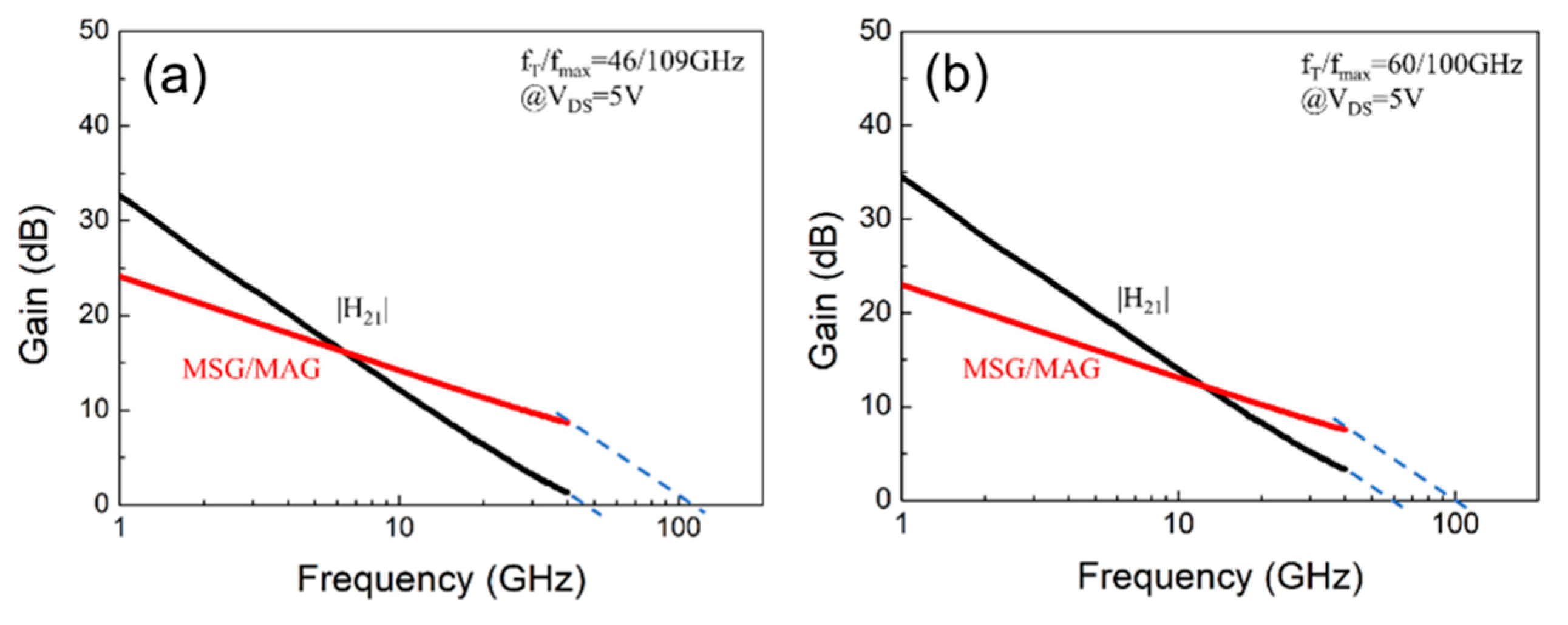
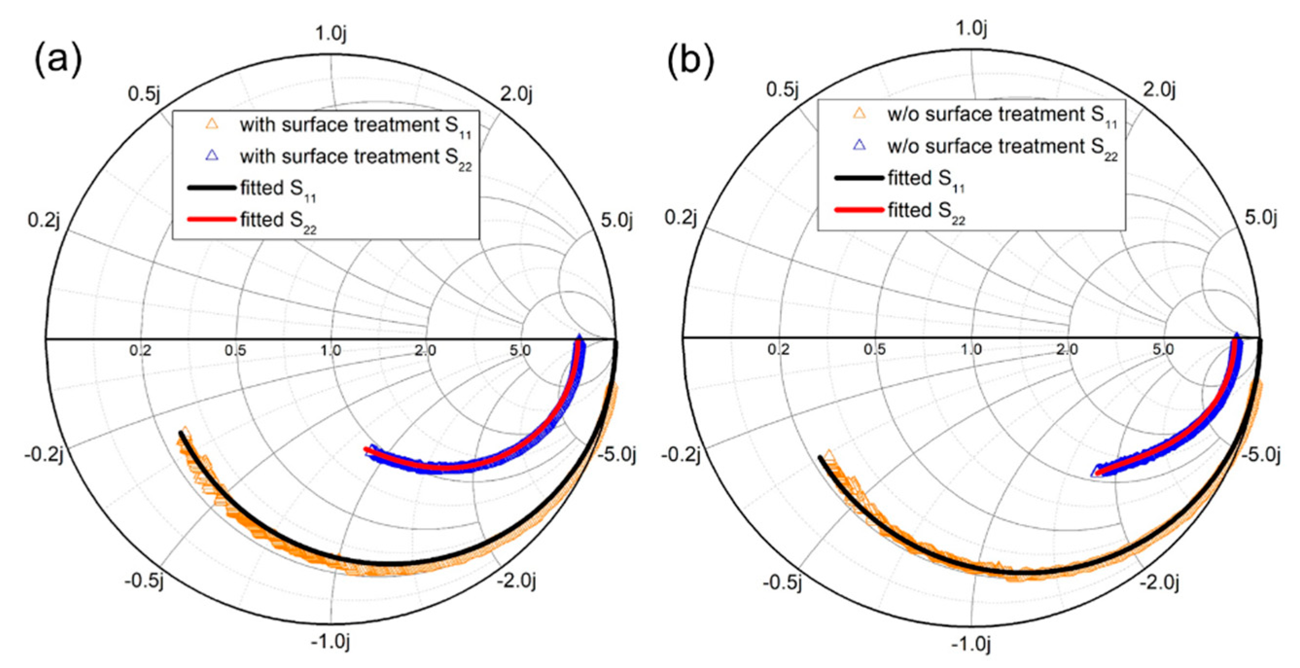
3.3. Small-Signal Characteristics Comparison

The small-signal RF S-parameters were measured from 100 MHz to 40 GHz using a Keysight N5227B network analyzer. A standard short-open-load-through (SOLT) calibration method was adopted to calibrate the system with the reference planes set at the tips of the corresponding probes. Figure 10 shows the measurement results for the devices with and without wet surface treatment. The extracted unit current-gain cutoff frequency (fT) and the maximum oscillation frequency (fmax) were 46/60 GHz and 109/100 GHz for the device with/without surface treatment. We have used the small-signal equivalent circuit using the procedure in [24] to extract parameters. Figure 11 shows that there is no difference between the Smith chart of the measured and fitted curves. The total gate capacitance (Cgs + Cgd) for devices without and with surface treatment are 98.95 fF and 86.7 fF, respectively. Thus, the higher cut-off frequency (fT) of the device with wet surface treatment can be attributed to the lower gate capacitance. However, slight degradation in fmax for the device with surface treatment is possibly due to the decrease of the output current and the lower 2DEG density.

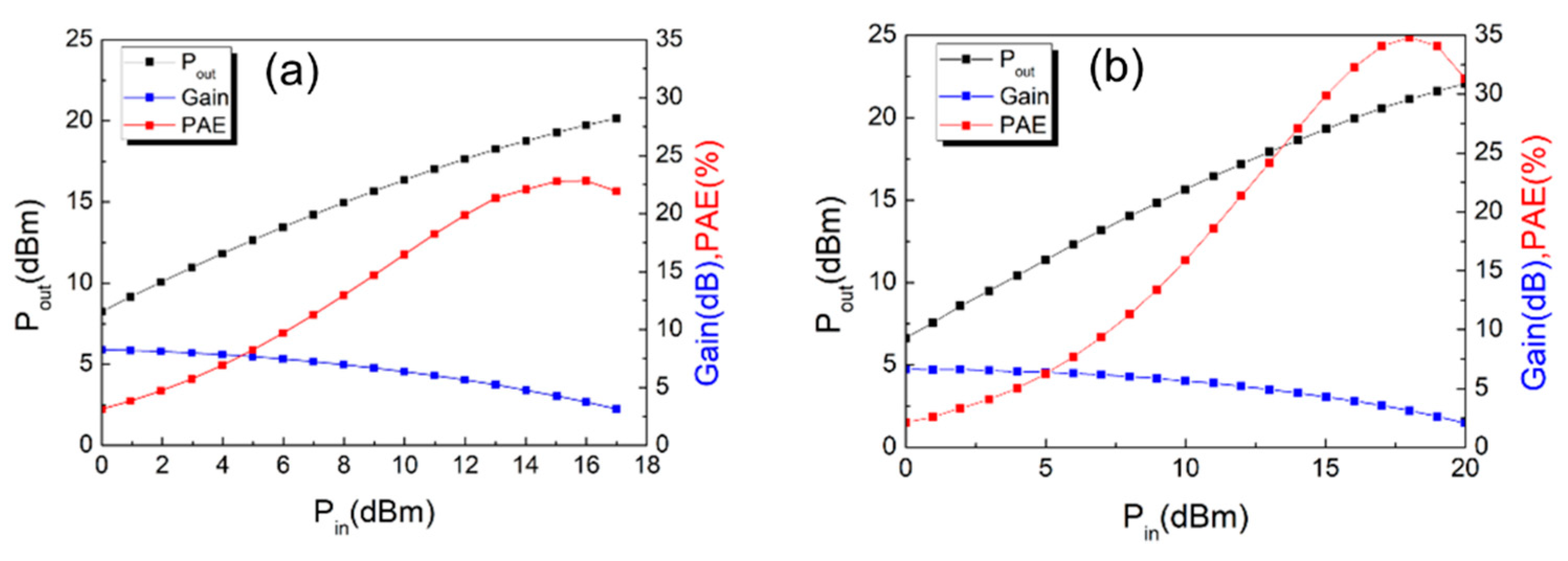
3.4. Large-Signal Performance

The large-signal performance was characterized using an on-wafer load-pull system at 38 GHz under continuous mode excitation. Figure 12 shows the measurement results with the device biased at class AB operation and the impedance is optimized for maximum output power. The optimal source and load impedance for the device without treatment are (32.20 + j24.12) Ω and (92.15 + j126.12) Ω and those for the device with treatment are (35.85 + j28.31) Ω and (226.07 + j216.15) Ω, respectively. Under these conditions, a maximum output power density of 2.1 W/mm with a linear power gain (Gp) of 8.2 dB and a PAE of 22.84% were obtained at VDS = 10 V for the device without wet surface treatment. On the other hand, with the suppression of current collapse, a higher maximum output power density of 3.22 W/mm and a PAE of 34.83% were achieved for the device with surface treatment. Such a substantial improvement in the performance at Ka-band is mainly attributed to the suppression of the current collapse issue [25]. The measurement results have evidenced that the device technology presented in this paper is promising for future applications in power amplifiers at millimeter-wave frequencies. Furthermore, the proposed MOSHEMT outperforms other E-mode AlGaN/GaN HEMTs on SiC substrate [4,7,26]. The reported work exhibits a good power performance at relatively low VDS. In all, the experimental results of the thin barrier E-mode AlGaN/GaN HEMT on Sapphire shows a great potential for low power consumption and low-cost power amplifier application.

4. Conclusions

A high-performance thin barrier enhancement-mode AlGaN/GaN HEMT was fabricated with wet surface treatment and high-quality Al2O3 as the gate dielectric layer. After the dry etching process and wet etching treatment, the damaged surface layer was removed. Moreover, the current collapse was eliminated due to the reduced trapping effect. Compared to a device without surface treatment, substantial improvement in the radiofrequency (RF) performance was achieved. The device exhibited a superior power performance, including a maximum output power density of 3.22 W/mm and a peak PAE of 34.83% at 38 GHz. These results demonstrate an attractive technique for fabricating high-performance E-mode HEMTs for power amplifier applications at millimeter-wave frequencies.

Author Contributions

Experiment, C.W. and Y.-C.C.; Analysis and writing, C.W.; Conceiving the idea, review and editing, H.-T.H., Y.-C.L., E.-Y.C. and C.-F.D.; Data curation, C.W. and Y.-C.C.; DC data analysis, C.W. and Y.-C.L.; RF measurement, H.-T.H. and Y.-F.T.; RF data analysis, C.W., H.-T.H. and Y.-F.T.; supervision, E.-Y.C. and C.-F.D. All authors have read and agreed to the published version of the manuscript.

Funding

This work was financially supported by the “Center for the Semiconductor Technology Research” from The Featured Areas Research Center Program within the framework of the Higher Education Sprout Project by the Ministry of Education (MOE) in Taiwan. Also, it is supported in part by the Ministry of Science and Technology, Taiwan, under Grant MOST 110-2634-F-009-027- as well as 110-2622-8-009-018-SB.

Institutional Review Board Statement

Not applicable.

Informed Consent Statement

Not applicable.

Data Availability Statement

The data presented in this paper are available on request from the corresponding author.

Conflicts of Interest

The authors declare no conflict of interest.

References

  1. Palacios, T.; Chakraborty, A.; Rajan, S.; Poblenz, C.; Keller, S.; DenBaars, S.P.; Speck, J.S.; Mishra, U.K. High-power AlGaN/GaN HEMTs for Ka-band applications. IEEE Electron Device Lett. 2005, 26, 781–783. [Google Scholar] [CrossRef] [Green Version]
  2. Harrouche, K.; Kabouche, R.; Okada, E.; Medjdoub, F. High Performance and Highly Robust AlN/GaN HEMTs for Millimeter-Wave Operation. IEEE J. Electron Devices Soc. 2019, 7, 1145–1150. [Google Scholar] [CrossRef]
  3. Aubry, R.; Jacquet, J.C.; Oualli, M.; Patard, O.; Piotrowicz, S.; Chartier, E.; Michel, N.; Xuan, L.T.; Lancereau, D.; Potier, C.; et al. ICP-CVD SiN Passivation for High-Power RF InAlGaN/GaN/SiC HEMT. IEEE Electron Device Lett. 2016, 37, 629–632. [Google Scholar] [CrossRef]
  4. Feng, Z.H.; Zhou, R.; Xie, S.Y.; Yin, J.Y.; Fang, J.X.; Liu, B.; Zhou, W.; Chen, K.J.; Cai, S.J. 18-GHz 3.65-W/mm Enhancement-Mode AlGaN/GaN HFET Using Fluorine Plasma Ion Implantation. IEEE Electron Device Lett. 2010, 31, 1386–1388. [Google Scholar] [CrossRef]
  5. Yu, C.J.; Hsu, C.W.; Wu, M.C.; Hsu, W.C.; Chuang, C.Y.; Liu, J.Z. Improved DC and RF Performance of Novel MIS p-GaN-Gated HEMTs by Gate-All-Around Structure. IEEE Electron Device Lett. 2020, 41, 673–676. [Google Scholar] [CrossRef]
  6. Moon, J.; Wu, S.; Wong, D.; Milosavljevic, I.; Conway, A.; Hashimoto, P.; Hu, M.; Antcliffe, M.; Micovic, M. Gate-Recessed AlGaN–GaN HEMTs for High-Performance Millimeter-Wave Applications. IEEE Electron Device Lett. 2005, 26, 348–350. [Google Scholar] [CrossRef]
  7. Maroldt, S.; Haupt, C.; Pletschen, W.; Müller, S.; Quay, R.; Ambacher, O.; Schippel, C.; Schwierz, F. Gate-Recessed AlGaN/GaN Based Enhancement-Mode High Electron Mobility Transistors for High Frequency Operation. Jpn. J. Appl. Phys. 2009, 48, 04C083. [Google Scholar] [CrossRef]
  8. Schuette, M.L.; Ketterson, A.; Song, B.; Beam, E.; Chou, T.M.; Pilla, M.; Tserng, H.Q.; Gao, X.; Guo, S.; Fay, P.J.; et al. Gate-Recessed Integrated E/D GaN HEMT Technology With fT / fmax >300 GHz. IEEE Electron Device Lett. 2013, 34, 741–743. [Google Scholar] [CrossRef]
  9. Makiyama, K.; Ozaki, S.; Ohki, T.; Okamoto, N.; Minoura, Y.; Niida, Y.; Kamada, Y.; Joshin, K.; Watanabe, K.; Miyamoto, Y. Collapse-free high power InAlGaN/GaN-HEMT with 3 W/mm at 96 GHz. In Proceedings of the International Electron Devices Meeting (IEDM), Washington, DC, USA, 7–9 December 2015; pp. 9.1.1–9.1.4. [Google Scholar]
  10. Kim, D.; Kumar, V.; Lee, J.; Yan, M.; Dabiran, A.M.; Wowchak, A.M.; Chow, P.P.; Adesida, I. Recessed 70-nm gate-length AlGaN/GaN HEMTs fabricated using an Al2O3/SiNx dielectric layer. IEEE Electron Device Lett. 2009, 30, 913–915. [Google Scholar]
  11. Huang, S.; Liu, X.; Zhang, J.; Wei, K.; Liu, G.; Wang, X.; Zheng, Y.; Liu, H.; Jin, Z.; Zhao, C.; et al. High RF performance enhancement-mode Al2O3/AlGaN/GaN MIS-HEMTs fabricated with high-temperature gate-recess technique. IEEE Electron Device Lett. 2015, 36, 754–756. [Google Scholar] [CrossRef]
  12. Lin, Y.-K.; Noda, S.; Huang, C.-C.; Lo, H.-C.; Wu, C.-H.; Luc, Q.H.; Chang, P.-C.; Hsu, H.-T.; Samukawa, S.; Chang, E.Y. High-performance GaN MOSHEMTs fabricated with ALD Al2O3 Dielectric and NBE gate recess technology for high frequency power applications. IEEE Electron Device Lett. 2017, 38, 771–774. [Google Scholar] [CrossRef]
  13. Zhang, Y.; Huang, S.; Wei, K.; Zhang, S.; Wang, X.; Zheng, Y.; Liu, G.; Chen, X.; Li, Y.; Liu, X. Millimeter-wave AlGaN/GaN HEMTs with 43.6% power-added-efficiency at 40 GHz fabricated by atomic layer etching gate recess. IEEE Electron Device Lett. 2010, 41, 701–704. [Google Scholar] [CrossRef]
  14. Mi, M.; Ma, X.-H.; Yang, L.; Lu, Y.; Hou, B.; Zhu, J.; Zhang, M.; Zhang, H.-S.; Zhu, Q.; Yang, L.-A.; et al. Millimeter-wave power AlGaN/GaN HEMT using surface plasma treatment of access region. IEEE Trans. Electron Devices 2017, 64, 4875–4881. [Google Scholar] [CrossRef]
  15. Mi, M.-H.; Ma, X.-H.; Yang, L.; Hou, B.-; Zhu, J.-J.; He, Y.-L.; Zhang, M.; Wu, S.; Hao, Y. 90 nm gate length enhancement-mode AlGaN/GaN HEMTs with plasma oxidation technology for high-frequency application. Appl. Phys. Lett. 2017, 111, 173502. [Google Scholar] [CrossRef]
  16. Tingting, Y.; Xinyu, L.; Yingkui, Z.; Chengzhan, L.; Ke, W.; Guoguo, L. Impact of UV/ozone surface treatment on AlGaN/GaN HEMTs. J. Semicond. 2009, 30, 124001. [Google Scholar] [CrossRef]
  17. Do, J.-W.; Jung, H.-W.; Shin, M.J.; Ahn, H.-K.; Kim, H.; Kim, R.-H.; Cho, K.J.; Chang, S.-J.; Min, B.-G.; Yoon, H.S.; et al. The effects of tetramethylammonium hydroxide treatment on the performance of recessed-gate AlGaN/GaN high electron mobility transistors. Thin Solid Films 2017, 628, 31–35. [Google Scholar] [CrossRef]
  18. Lee, N.-H.; Lee, M.; Choi, W.; Kim, D.; Jeon, N.; Choi, S.; Seo, K.-S. Effects of various surface treatments on gate leakage, subthreshold slope, and current collapse in AlGaN/GaN high-electron-mobility transistors. Jpn. J. Appl. Phys. 2014, 53, 04EF10. [Google Scholar] [CrossRef] [Green Version]
  19. Bardwell, J.; Haffouz, S.; McKinnon, R.; Storey, C.; Tang, H.; Sproule, G.I.; Roth, D.; Wang, R. The effect of surface cleaning on current collapse in AlGaN/GaN HEMTs. Electrochem. Solid-State Lett. 2007, 10, H46–H49. [Google Scholar] [CrossRef]
  20. Wang, L.; Bu, Y.; Ao, J.-P. Effect of oxygen plasma treatment on the performance of AlGaN/GaN ion-sensitive field-effect transistors. Diam. Relat. Mater. 2017, 73, 1–6. [Google Scholar] [CrossRef]
  21. Liu, S.C.; Chen, B.Y.; Lin, Y.C.; Hsieh, T.E.; Wang, H.C.; Chang, E.Y. GaN MIS-HEMTs with nitrogen passivation for power device application. IEEE Electron Device Lett. 2014, 35, 1001–1003. [Google Scholar]
  22. Desmaris, V.; Rudzinski, M.; Rorsman, N.; Hageman, P.; Larsen, P.; Zirath, H.; Rodle, T.; Jos, H. Comparison of the DC and microwave performance of AlGaN/GaN HEMTs grown on SiC by MOCVD with Fe-doped or unintentionally doped GaN buffer layers. IEEE Trans. Electron Devices 2006, 53, 2413–2417. [Google Scholar] [CrossRef]
  23. Meneghini, M.; Rossetto, I.; Bisi, D.; Stocco, A.; Chini, A.; Pantellini, A.; Lanzieri, C.; Nanni, A.; Meneghesso, G.; Zanoni, E. Buffer traps in Fe-doped AlGaN/GaN HEMTs: Investigation of the physical properties based on pulsed and transient measurements. IEEE Trans. Electron Devices 2014, 61, 4070–4077. [Google Scholar] [CrossRef]
  24. Jarndal, A.; Kompa, G. A New Small-Signal Modeling Approach Applied to GaN Devices. IEEE Trans Microwave Theory Tech. 2005, 53, 3440–3448. [Google Scholar] [CrossRef]
  25. Lin, S.; Wang, M.; Xie, B.; Wen, C.P.; Yu, M.; Wang, J.; Hao, Y.; Wu, W.; Huang, S.; Chen, K.J.; et al. Reduction of current collapse in GaN high-electron mobility transistors using a repeated ozone oxidation and wet surface treatment. IEEE Electron Device Lett. 2015, 36, 757–759. [Google Scholar]
  26. Ohki, T.; Kikkawa, T.; Kanamura, M.; Imanishi, K.; Makiyama, K.; Okamoto, N.; Joshin, K.; Hara, N. An over 100 W AlGaN/GaN enhancement-mode HEMT power amplifier with piezoelectric-induced cap structure. Phys. Stat. Solidi (C) 2009, 6, 1365–1368. [Google Scholar] [CrossRef]
Figure 1. (a) Epitaxial structure and (b) scanning electron microscopy (SEM) image of the T-shape gate for the thin barrier AlGaN/GaN metal-oxide-semiconductor high-electron-mobility transistor (MOSHEMT).
Materials 14 06558 g001
Figure 2. (a) Scanning electron microscope (SEM) image of top view of the high-electron-mobility transistor (HEMT) device and (b) SEM image of the magnification of the Source/Drain spacing region.
Materials 14 06558 g002
Figure 3. Energy-dispersive X-ray spectroscopy (EDX) analysis of (a) aluminum and (b) gallium element.
Materials 14 06558 g003
Figure 4. The cross-section high-resolution transmission electron microscopy (HRTEM) image of the interface.
Materials 14 06558 g004
Figure 5. Fabrication process for the thin barrier E-mode AlGaN/GaN MOSHEMT.
Materials 14 06558 g005
Figure 6. Surface morphology of the AlGaN/GaN heterostructure after etching barrier layer (a) without treatment and (b) with wet surface treatment.
Materials 14 06558 g006
Figure 7. The X-ray photoelectron spectroscopy (XPS): (a) Ga 3d and (b) Al 2p core level spectra of the AlGaN surface with and without wet surface treatment.
Materials 14 06558 g007
Figure 8. (a) The measured drain current as functions of drain voltage for devices with and without surface treatment. (b) The measured drain current and extrinsic transconductance (gm) with surface treatment. (c) Gate leakage of recess gate HEMTs with and without surface treatment.
Materials 14 06558 g008
Figure 9. Pulsed I–V characterization with 200-ns pulse width and 0.1% duty cycle for 2 × 25 μm2 thin barrier AlGaN/GaN HEMTs (a) without and (b) with wet surface treatment.
Materials 14 06558 g009
Figure 10. The extracted cut-off frequency (fT) and maximum oscillation frequency (fmax) for thin barrier AlGaN/GaN MOSHEMT devices: (a) without and (b) with surface treatment.
Materials 14 06558 g010
Figure 11. The Smith chart of the measured and fitted curves of the (a) with and (b) without surface treatment device.
Materials 14 06558 g011
Figure 12. Large signal radiofrequency (RF) output power characteristics of (a) without (b) with wet surface treatment (VDS = 10 V) at 38 GHz.
Materials 14 06558 g012
Publisher’s Note: MDPI stays neutral with regard to jurisdictional claims in published maps and institutional affiliations.

