Abstract
A three-phase isolated rectifier features bidirectional power conversion and galvanic isolation, and is attractive as a high-efficiency energy conversion system. However, when a conventional modulation is applied to this rectifier, the excessive DC-link current ripple will result in increasing switching losses or the size of DC-link inductance, which is not cost-effective. In order to effectively reduce the current ripple, this paper proposes a “six segment” PWM (Pulse Width Modulation) strategy. It can significantly reduce the current ripple compared with the existing “eight segment” PWM strategy. Meanwhile, the current quality of the grid is improved. Finally, the experimental tests were carried out. The experimental results reveal that, compared to the traditional “eight segment” PWM, the dc-side current ripple significantly reduced from 2 A to 0.8 A, the total harmonic distortion significantly reduced from 5.69% to 2.41%, and the power factor increased from 0.87 to 0.99, verifying the effectiveness of the proposed method.
1. Introduction
Nowadays, high-efficiency energy conversion systems are more and more demanding. As for the dc microgrid, most electrical equipment is of a DC load, meaning an alternating current (AC) directly introduced from the utility cannot meet the requirements of the load. It is necessary to convert the AC into a direct current (DC) by high-efficiency energy conversion. The power rectifier that converts an alternating current to direct current is called a rectifier. Acting as a rectifier between power grid and powered devices, it has been widely used in communication power supply, photovoltaic system [1] and electric vehicle [2]. However, the power rectifier may produce a large number of harmonics, reduce the system efficiency and power quality, and may even endanger the safe operation of the grid [3,4]. Therefore, it is necessary to reduce and suppress the undesirable harmonics. At present, harmonics are mainly suppressed by directly installing filters at a certain area for harmonic compensation or improving power electronic rectifiers that produce harmonics. The harmonics restrain method of the former includes the installation of active and passive power filters. The latter mainly optimizes the topology and control strategy, that is, power-factor correction technology is adopted [5]. Active power-factor correction can lead to a high power factor, suppress harmonics and greatly reduce the volume by controlling switching devices. That is why it is the most widely used PFC (Power Factor Correction) circuit at present. Generally, it can be divided into two categories according to topology and energy flow direction [6,7].
From the perspective of safety and reliability, it is usually required that the rectifier has the function of galvanic isolation. Therefore, a three-phase isolated matrix rectifier with a high-frequency transformer (HFT) is widely used as a typical PFC circuit due to its superior performance in areas such as power-factor correction [8,9,10], high power density, and low harmonic current distortion [11,12]. Therefore, three-phase isolated matrix rectifiers have broad application in the fields of electric vehicles, photovoltaic power generation systems, grid-connected rectifiers [13], micro grids [14], fuel cell power systems and in battery chargers [15]. The buck-derived matrix rectifier [16,17] can be a potential choice, especially when the input line voltage is high and the buck-derived matrix rectifier is also favorable in instances of a wide-ranging DC voltage. In addition, the buck topology has the advantages of a better dynamic response and no starting problems [18]. The DC bus of the rectifier in [17] varies at every 60◦ interval, since the DC bus is one of the three line-to-line voltages. These variations in line-to-line voltage within each sector contribute to larger output inductor current ripple. Therefore, a larger output inductor is required to limit the ripple current, which in turn decreases the power density of the rectifier. Due to the large output inductance of the ‘eight-segment’ PWM modulation strategy proposed in [17], this paper proposes a ‘six segment’ PWM scheme to solve the above-mentioned technical issue.
The rest of this paper is organized as follows: In Section 2, the circuit topology and the operating principles of the two modulation schemes are described. Then, in Section 3, the current ripple of the two schemes is analyzed. The result shows that the current ripple of the six segment PWM modulation is smaller. Following that, the simulation and experiment results for three-phase isolated matrix rectifiers are provided to compare the performance of different SVPWM strategies in Section 4 and Section 5. Finally, conclusions are drawn in Section 6.
2. System Configuration and Operation Principle
The topology of the three-phase isolated rectifier is shown in Figure 1. The rectifier contains a matrix rectifier (MC), high-frequency transformer (HFT) and uncontrolled rectifier bridge. The MC is composed of six bidirectional switches, which can facilitate a bidirectional current flow. The HFT connect the MC and the uncontrolled rectifier bridge, which allows for electrical isolation and energy transfer. The diodes of the uncontrolled rectifier bridge can be replaced with controllable switches to achieve bi-directional power flow. The Lf and Cf are used as a filter to filter high-frequency harmonics of the AC-side current. The inductor L and the capacitor C form an LC filter on the DC side.
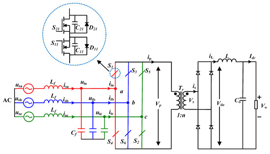
Figure 1.
The schematic diagram of three-phase isolated Rectifier.
As shown in Figure 1, the structure of the grid side MC is equivalent to a conventional CSR-based rectifier, except that the MC uses bidirectional switches, and therefore, the conventional SVPWM can be adopted to control this rectifier [19]. In order to maintain the flux balanced in HFT [20], the average voltage vector over a switching cycle is zero. Therefore, the switching vectors should produce alternating positive and negative primary voltage of the HFT. Consequently, two switching states depending on the direction of the primary side current Ip for each vector are required to correspond to the positive and negative current vector, respectively. The current space vector distribution in the two cases of Ip > 0 and Ip < 0 is shown in Figure 2, where Iref represents for the reference current.
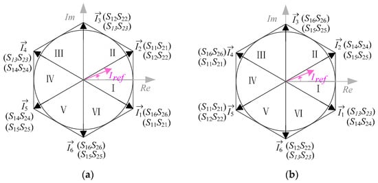
Figure 2.
Current space vector (a) Ip > 0, (b) Ip < 0.
Using bidirectional switch S1 (including S11 and S21, the same applies below, S12 and S22 are merged as a simple switch S2), the different switch states of S2, S3, S4, S5, and S6 cause the circuit output to alternate between positive and negative voltages Uab, Uac, Ubc, Uba, Uca, Ucb and zero voltage Uaa, Ubb, Ucc. The switching state and the corresponding output voltage are listed in Table 1.

Table 1.
The corresponding switch state of the space vector.
Active vectors I1 to I6 represent the active switching state, and zero switching states can be represented by zero space vectors I7, I8, and I9. As shown in Figure 2, for each of the active vectors, there are two possible switching states according to the direction of the primary side current Ip of the transformer. According to the different switching states, the six active vectors can be expressed by (1).
where n = 1, 2, …, 6 for sectors I, II, …, VI, respectively.
The reference vector rotates in space at the same angular velocity as the grid voltage vector to obtain a sinusoidal input current. is represented by two adjacent active vectors, , and a zero vector, as shown in Figure 3.
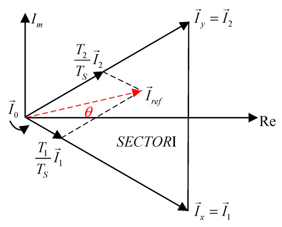
Figure 3.
Synthesis principle of reference vector Iref.
For the analysis in this section, take sector I for example, where the reference vector is composed of , and . Assuming that the output inductor current is constant, and it is balanced based on the ampere-second principle:
where T1, T2 and T0 are the dwell times of the vectors , and , respectively. Ts is the switching cycle. Additionally, the dwell times of each vector can be calculated by (3)
where ma is the modulation factor, given by
where Im is the amplitude of the fundamental component of the grid current.
Take the interval as an example, the voltage waveforms and the switching states of the existing ‘eight-segment’ PWM modulation strategy proposed in [17] are shown in Figure 4. The power switches (S1, S6) are turned on firstly, and the output voltage is VAB. In order to maintain the transformer flux balanced, a reverse voltage VBA with the same amplitude can be generated by turning on switches (S1, S6). Additionally, the zero vector states are added during the transition of the positive and negative voltages to ensure minimum switching during the switching state. That is to say, the principle of the ‘eight-segment’ strategy can be summarized as inserting a uniformly distributed zero vector between every two output voltages, and leads to the output alternating between a positive and negative voltage.
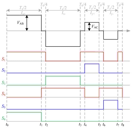
Figure 4.
Waveforms of the primary voltage and switching states of ‘eight segment’ SVM.
However, the ‘eight segment’ SVM has the disadvantage of a large output inductor current ripple, and therefore, a large inductor is required on the DC side to suppress the ripple current. In order to address this issue, this article uses a ‘six segment’ PWM modulation method to reduce the output inductor current ripple by changing the switching state.
Take the interval as an example, the voltage waveforms and the switching states of the proposed ‘six-segment’ PWM modulation strategy are shown in Figure 5. Based on the above working principle, first turn on the switches (S1, S6) to the output voltage VAB, and then turn on the switches (S1, S2) to output voltage VAC. In order to keep the transformer flux balanced, the negative voltage VBA and VCA of the same amplitude with VAB and VAC needs to be generated. The zero vectors are equally divided into two parts in this working state and inserted between the alternating positive and negative voltage outputs to form an AC voltage step wave.
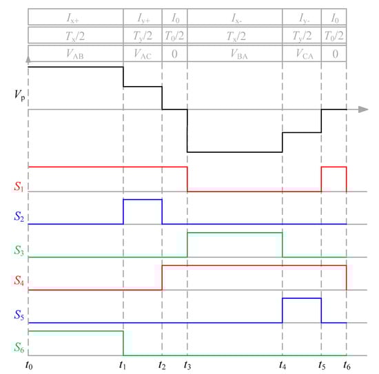
Figure 5.
Waveforms of the primary voltage and switching states of ‘six segment’ SVM.
3. DC-Link Current Ripple Analysis
The inductor current ripple affects the DC output filter inductance. If the current ripple is small, the small inductance can meet the filtering requirements, a corresponding increase in the power density of the system occurs.
For a given output voltage, the DC-inductor current ripple depends on the total turn-off time of the output voltage Vd and the division method of the turn-off time within a switch period. For the “eight-segment” PWM modulation mode, the four zero vectors are evenly distributed in one switching period, while for the “six segment” PWM modulation mode, the zero vectors are equally divided into two parts to separate the alternating positive and negative output voltages. Theoretically, the output inductor current ripple iL rises slowly when Vd turns on, and decreases slowly when Vd turns off. As shown in Figure 6, the schematic diagrams of output filter inductor current ripple at , , and , respectively.
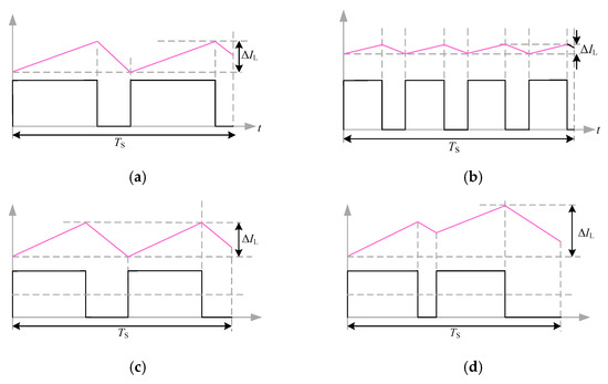
Figure 6.
Inductor current ripple. (a) “six segment” current ripple, (b) “eight segment” current ripple, (c) “six segment” current ripple, (d) “eight segment” current ripple.
Since the turn-off time of Vd varies, when , the turn-off time of Vd is the smallest. The “six segment “ consists of two voltage square waves of equal amplitude, and the “eight-segment type” consists of four voltage square waves of equal amplitude. The total turn-off time is (1 − ma) Ts, the ripple current at this time is the smallest, and the current ripple expression is given as follows.
At , the “six segment” is composed of two voltage square waves of equal amplitude, there are only two zero vector intervals, and the total off time reaches the maximum () Ts. At this time, the current has also reached the maximum, and the “eight-segment type” is also composed of two voltage square waves of equal amplitude, and the three turn-off intervals after the second voltage square wave are combined into one. The current ripple expression is as follows:
According to (5) and (6), in the case of minimum ripple current, the current ripple generated by the “six segment” PWM modulation strategy is twice that of the “eight-segment” PWM modulation strategy; However, in the case of maximum current ripple (), the current ripple of the “six segment” PWM modulation strategy is significantly smaller than that of the “eight segment” PWM modulation strategy. When designing the LC filter inductor, it is necessary to calculate the L parameter with the maximum inductor current ripple. Therefore, the “six segment” PWM modulation strategy can reduce the volume of the output inductor and reduce costs while increasing power density.
4. Simulation Results
In order to verify the effectiveness of theoretical analysis, the ‘six segment’ and ‘eight segment’ PWM modulation strategies of the three-phase isolated rectifier are implemented and simulated in MATLAB/Simulink. The simulation parameters are listed in Table 2.
Table 2.
Experimental parameters.
Figure 7 shows the drive signal of the power switches under two different modulation modes. The two switches of the bidirectional switch on each bridge arm are equivalent to an ideal switch, and their driving signals are the same. At any time, there are two switches turned on at the same time.
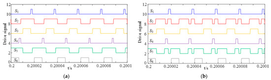
Figure 7.
Drive signals of switches. (a) ‘Six segment’ drive signal, (b) ‘Eight segment’ drive signal.
Figure 8 and Figure 9 show the waveforms of the output voltage of the primary and secondary side of the transformer in the two modulation modes. Comparing the simulation results, it can be seen that the waveforms of the primary and secondary voltages of transformers present three-phase high-frequency sinusoidal variation, and the voltage can maintain the same amplitude.
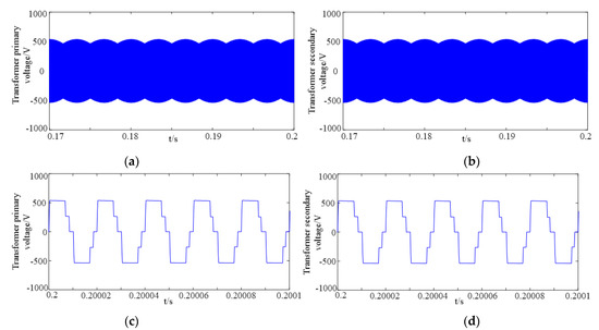
Figure 8.
Waveforms of primary and secondary voltage of the transform of ‘six segment’ SVM. (a) Primary voltage, (b) Secondary voltage, (c) Primary voltage (details), (d) Secondary voltage (details).
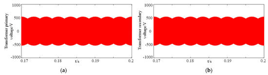
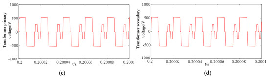
Figure 9.
Waveforms of primary and secondary voltage of the transform of ‘eight segment’ SVM. (a) Primary voltage, (b) Secondary voltage, (c) Primary voltage (details), (d) Secondary voltage (details).
Figure 10 shows the DC-inductance current ripple of the proposed ‘six segment’ SVM and ‘eight segment’ SVM. It can be clearly seen that the ripple current of the ‘six segment’ SVM (as shown in Figure 10a) is stable between the range of 7 A to 7.5 A, while the ripple current of the ‘eight segment’ SVM (as shown in Figure 10a,b) is stable between the range of 6.7 A to 8 A. That is, compared with the ‘eight segment’ SVM strategy, the peak–peak DC-link current ripple of the proposed ‘six segment’ SVM strategy is much smaller. This results in a high cost and performance ratio, as well as high power density.
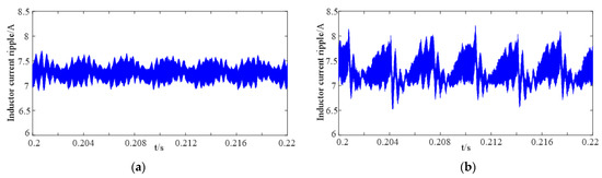
Figure 10.
Waveforms of inductor current ripple. (a) ‘six segment’ scheme, (b) ‘eight segment’ scheme.
Figure 11 shows the waveforms of the rectifier bridge output voltage and ripple current. It can be seen that the ripple current varies with the rectified output voltage. The peak value of the current ripple under the ‘eight-segment’ modulation is higher than the ‘six segment’ modulation. That is to say, the results are consistent with the theoretical analysis.
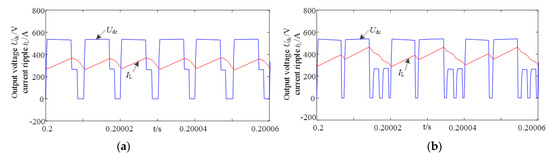
Figure 11.
Waveforms of output voltage and current ripple. (a) ‘six segment’ scheme, (b) ‘eight segment’ scheme.
It can be seen from Figure 12 that the grid-side current is sinusoidal for the traditional and proposed modulation methods. It also can been seen that the DC output voltage can accurately track the reference value. From Figure 12b,d, the current ripple of the DC filter inductor current IL of the ‘six segment’ scheme is much smaller than that of the ‘eight segment’ scheme. On the other hand, as shown in Figure 12e,f, the THD with the proposed six-segment scheme is lower with better power quality.
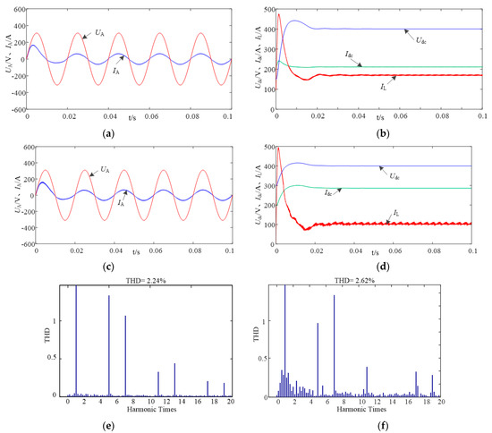
Figure 12.
AC-side voltage and current waveform, output voltage and THD. (a) Voltage and current by six segment, (b) Output of six segment, (c) Voltage and current by eight segment, (d) Output of eight segment, (e) “Six segment” THD, (f) “Eight segment” THD.
5. Experimental Results
To verify the proposed six-segment strategy for the three-phase isolated rectifier, a down-scaled prototype was built. Texas Instruments DSP TMS320F28335 and FPGA XC6SLX9-2TQG144C were used to implement the control algorithm. Detailed parameters of the experiment are listed in Table 3.
Table 3.
Experimental parameters.
Figure 13 shows the phase-locked waveform of three-phase isolated PFC. According to the experimental results, the phase angle of phase-locked waveform follows the phase a voltage, and the phase angle cycle is consistent with the AC input voltage cycle, both of which are 0.02 s.
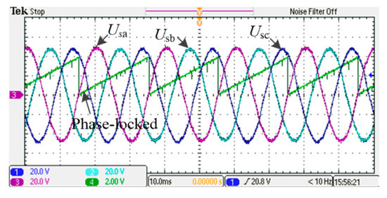
Figure 13.
The wave of three-phase phase-locked loop.
In the experiment, in order to prevent the circuit from losing the current loop at the moment of commutation, a stacking time of 2 μs was set for the switch drive, as shown in Figure 14. The figure, respectively, represents four switches drive signals. When the switch represented by channel 1 is turned on, the switch represented by channel 3 will always be turned off with a delay of 2 μs.
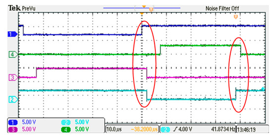
Figure 14.
Drive pulses for switches.
Figure 15 shows the voltage and current waveforms on the primary and secondary sides of the transformer. By observing the overall waveform, it can be seen that the voltage and current on the primary and secondary sides of the transformer exhibit high-frequency sinusoidal changes. It can be seen from the detailed diagram that the transformer current changes alternately positive and negative with the change of voltage.
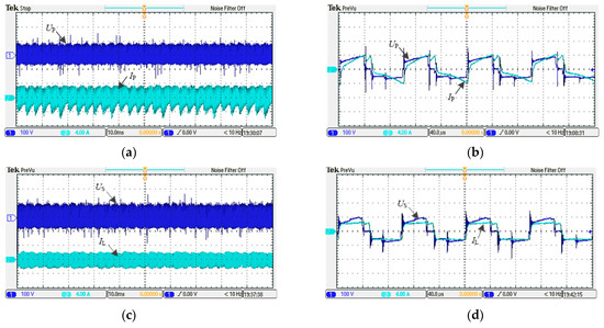
Figure 15.
Voltage and current waveforms of primary and secondary sides of transformer. (a) Primary waveform, (b) Primary waveform (details), (c) Secondary waveform, (d) Secondary waveform (details).
Figure 16 shows the voltage waveforms of the primary and secondary sides of the transformer under the eight segment PWM and six segment PWM modulation modes. It can be seen that the voltage at two sides of the transformer is a step wave alternating between positive and negative. Since the transformation ratio is 1:1, the voltage amplitude is roughly the same, which is consistent with the simulation analysis.
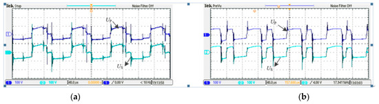
Figure 16.
Voltage waveform of primary and secondary sides of transformer. (a) “Six segment”, (b) “Eight segment”.
According to the DC output voltage and ripple current shown in Figure 17, the inductance current has a large ripple of 2 A under the ‘eight segment’ modulation mode. The inductance current ripple of 0.8 A in the ‘six segment’ modulation mode is significantly reduced by 60%.
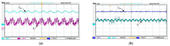
Figure 17.
Current ripple and output voltage. (a) “Eight segment”, (b) “Six segment”.
Figure 18a,b show the voltage and current waveforms at the grid side under the ‘six segment’ and ‘eight segment’ modulation modes, respectively. Compared with the ‘eight segment’ PWM modulation scheme, the ‘six segment’ PWM modulation scheme can improve the waveform quality of the grid current. The total harmonic distortion is significantly reduced from 5.69% to 2.41%, and the power factor increases from 0.87 to 0.99, which further verifies the effectiveness of the proposed method.
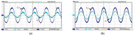
Figure 18.
Grid-side voltage and current waveforms. (a) “Eight segment”, (b) “Six segment”.
6. Conclusions
This paper has presented a new six-segment modulation scheme for a three-phase isolated rectifier. After experimental verification, the following conclusions are drawn: By adopting the proposed modulation strategy, the output waveform of the primary and secondary sides of the transformer presents high-frequency sinusoidal changes, and the details are displayed as positive and negative alternating trapezoidal waves. Compared with the traditional ‘eight segment’ scheme, the current ripple of the output inductor under the proposed ‘six segment’ PWM scheme is significantly reduced from 2 A to 0.8 A, the total harmonic distortion is significantly reduced from 5.69% to 2.41%, and the power factor increases from 0.87 to 0.99, which verifies the effectiveness of the proposed method. The limitation of the proposal is that the digital implementation needs a coordinated operation between DSP and FPGA, which increase the computational burden. With the rapid development of DSP and FPGA, the computational burden would not be a decisive factor. Therefore, the proposed method is valuable for future applications.
Author Contributions
Conceptualization, H.W.; methodology, H.W., S.W., C.S., D.J., C.C. and J.M.G.; validation, H.W., S.W. and C.S.; investigation, H.W., S.W., C.S., D.J., C.C. and J.M.G.; writing—original draft preparation, H.W., S.W. and C.S.; writing—review and editing, H.W., S.W., C.S., D.J., C.C., H.D. and J.M.G.; supervision, C.S., D.J., C.C., H.D. and J.M.G.; project administration, C.S., D.J., C.C., H.D. and J.M.G. All authors have read and agreed to the published version of the manuscript.
Funding
This work was supported by the National Key Research and Development Program of China (2021YFB2601600), Hebei Province Natural Science Foundation (F2020203013), Hebei Province 333 Talent Program (A202005001) and National Natural Science Foundation of China (61903321).
Institutional Review Board Statement
Not applicable.
Informed Consent Statement
Not applicable.
Data Availability Statement
Not applicable.
Conflicts of Interest
The authors declare no conflict of interest.
References
- Sikorski, A.; Falkowski, P.; Korzeniewski, M. Comparison of Two Power Converter Topologies in Wind Turbine System. Energies 2021, 14, 6574. [Google Scholar] [CrossRef]
- Nam, V.-H.; Tinh, D.-V.; Choi, W. A Novel Hybrid LDC Converter Topology for the Integrated On-Board Charger of Electric Vehicles. Energies 2021, 14, 3603. [Google Scholar] [CrossRef]
- Zou, N.; Yan, Y.; Shi, T.; Song, P. Wide Speed Range Operation Strategy of Indirect Matrix Converter–Surface Mounted Permanent Magnet Synchronous Motor Drive. Energies 2021, 14, 2277. [Google Scholar] [CrossRef]
- García, O.; Cobos, J.A.; Prieto, R.; Alou, P.; Uceda, J. Single Phase Power Factor Correction: A Survey. IEEE Trans. Power Electron. 2003, 18, 749–755. [Google Scholar] [CrossRef] [Green Version]
- Zhang, Z.; Xu, C.; Liu, Y.F. A Digital Adaptive Discontinuous Current Source Driver for High-Frequency Interleaved BoostPFC Converters. IEEE Trans. Power Electron. 2014, 29, 1298–1310. [Google Scholar] [CrossRef]
- Tsai, J.-R.; Wu, T.-F.; Wu, C.-Y.; Chen, Y.-M. Interleaving phase shifts for critical-mode boost PFC. IEEE Trans. Power Electron. 2008, 23, 1348–1357. [Google Scholar] [CrossRef]
- Robeiro, H.; Borges, B. New optimized full bridge, single-stage AC/DC converters. IEEE Trans. Ind. Electron. 2011, 6, 2397–2409. [Google Scholar] [CrossRef]
- Casadei, D.; Serra, G.; Tani, A.; Zari, L. Matrix converter modulation strategies: A new general approach based on space-vector representation of the switching state. IEEE Trans. Ind. Electron. 2002, 49, 370–381. [Google Scholar] [CrossRef]
- Nguyen, T.D.; Lee, H. Modulation Strategies to reduce common-mode voltage for indirect matrix converters. IEEE Trans. Ind. Electron. 2012, 59, 129–140. [Google Scholar] [CrossRef]
- Rivera, M.; Wilson, A.; Rojas, C.A.; Rodrigez, J.; Espinoza, J.R.; Wheeler, P.W.; Empringham, L. A comparative assessment of model predictive current control and space vector modulation in a direct matrix converter. IEEE Trans. Ind. Electron. 2013, 60, 578–588. [Google Scholar] [CrossRef]
- Rodriguez, J.; Rivera, M.; Kolar, J.W.; Wheeler, P.W. A review of control and modulation methods for matrix converters. IEEE Trans. Ind. Electron. 2012, 59, 58–70. [Google Scholar] [CrossRef]
- Alesina, A.; Venturini, M.G.B. Analysis and design of optimum-amplitude nine-switch direct AC-AC converter. IEEE Trans. Power. Electron. 1989, 4, 101–112. [Google Scholar] [CrossRef]
- Vazquez, S.; Lukic, S.M.; Galvan, E.; Franquelo, L.G.; Carrasco, J.M. Energy storage systems for transport and grid applications. IEEE Trans. Ind. Electron. 2010, 57, 3881–3895. [Google Scholar] [CrossRef] [Green Version]
- Bhuiyan, F.A.; Yazdani, A. Energy storage technologies for grid connected and off-grid power system applications. In Proceedings of the 2012 IEEE Electrical Power and Energy Conference, London, ON, Canada, 10–12 October 2012; pp. 303–310. [Google Scholar]
- Yilmaz, M.; Krein, P. Review of battery charger topologies, charging power levels and infrastructure for plug-in electric and hybrid vehicles. IEEE Trans. Power Electron. 2013, 28, 2151–2169. [Google Scholar] [CrossRef]
- Inagaki, K.; Furuhashi, T.; Ishiguro, A.; Ishida, M.; Okuma, S. A new PWM control method for AC to DC converters with high-frequency transformer isolation. IEEE Trans. Ind. Appl. 1993, 29, 486–492. [Google Scholar] [CrossRef]
- Latkovic, V.; Borojevic, D. Digital-signal-processor-based control of three- phase space vector modulated converters. IEEE Trans. Ind. Electron. 1994, 41, 326–336. [Google Scholar] [CrossRef]
- Stupar, A.; Friedli, T.; Minibock, J.; Kolar, J.W. Towards a 99% efficient three-phase buck-type PFC rectifier for 400-V dc distribution systems. IEEE Trans. Power Electron. 2012, 27, 1732–1744. [Google Scholar] [CrossRef]
- Li, X.; Wu, F.; Yang, G.; Liu, H.; Meng, F. Precise Calculation Method of Vector Dwell Times for Single-Stage Isolated Three-Phase Buck-Type Rectifier to Reduce Grid Current Distortions. IEEE J. Emerg. Sel. Top. Power Electron. 2020, 8, 4457–4466. [Google Scholar] [CrossRef]
- Fang, F.; Tian, H.; Li, Y. Coordination Control of Modulation Index and Phase Shift Angle for Current Stress Reduction in Isolated AC–DC Matrix Converter. IEEE Trans. Power Electron. 2021, 36, 4585–4596. [Google Scholar] [CrossRef]
Publisher’s Note: MDPI stays neutral with regard to jurisdictional claims in published maps and institutional affiliations. |
© 2022 by the authors. Licensee MDPI, Basel, Switzerland. This article is an open access article distributed under the terms and conditions of the Creative Commons Attribution (CC BY) license (https://creativecommons.org/licenses/by/4.0/).