Abstract
The development of single-phase symmetrical bipolar voltage gain matrix converters (MC) is growing rapidly as they find their application in power systems for dynamic restoration of line voltages, high voltage AC–DC converters, and variable frequency controllers for many industrial processes. However, the existing trend in matrix converter technology is a buck–boost operation that has inherently serious issues of high voltage and current surges or stresses. This is a big source of the high voltage and current rating of semiconductor switching devices. There is also a problem of high ripples both for voltage as well for current, requiring large size of filtering capacitors and inductors. The non-symmetrical control of the voltage gain increases the control complication. A large count of operating transistors is critical regarding their cost, size, and power conversion losses, as the space and cost required by their gate control circuits are much larger than the size and cost of the switching transistors. Thus, in this research work, a new single-phase MC is introduced only employing six fully controlled switching devices, ensuring similar operation or outputs as is obtained from the existing topologies that require the use of eight or more fully controlled switching devices, and the reduction by two or more switching transistors helps to compact the overall size and lower the overall cost. The separation in its voltage buck and boost operation enables smooth control of the voltage gain through duty cycle control. The low values of the voltage and current surges reduce the power rating and losses of the switching devices. The flow of the current in the filtering inductor is kept unidirectional to avoid the current interruption and reversal problem once the operation of the converter is abruptly switched from inverting to non-inverting and vice versa. All these factors are comprehensively detailed through the circuit’s description and comparative analysis. Simulation and practical results are presented to confirm the effectiveness of the developed circuit topology.
1. Introduction
1.1. Motivation
Single-phase bipolar voltage gain matrix converters find their application in various fields, such as variable speed drive systems, power systems, voltage step-up AC-to-DC converters, traction systems, and converters associated with wind turbines. The voltage variation in a power system is very critical for sensitive loads and sensitive control systems. The main source of this voltage deviation is the system’s faults, especially single line to ground. During this event, the voltage of the faulty line is decreased, and for non-faulty lines, voltage is boosted. To balance the system’s voltage, it is mandatory to add and subtract the voltage from the line voltage. This can only be possible if matrix converters connected with the lines have abilities to produce the non-inverted and inverted regulated outputs. In the same way, single-phase matrix converters are also attractive in applications where speed variation is required in some selected discrete steps. Such applications include traction systems, grinding mills, and steel rolling mills. By viewing the preceding discussion, it is concluded that the design and development of single-phase matrix converters is an attractive research area nowadays. These features lead us to develop a compact-sized bipolar voltage matrix converter.
1.2. Literature Review
AC–AC converters are used in various fields, from domestic to industrial applications. Their basic role is to govern the output rms voltage and frequency per the load requirement or application [1]. These applications may include the correction of grid voltage through the dynamic voltage restorer, variable speed control system, solid-state transformer, and wind power system connected to the grid [2]. The voltage variation or flocculation is critical for the operation of the critical load as they are very sensitive to this variation. This issue is very common in modern power systems due to the use of renewable energy resources or the presence of faults in the power system. For example, a single phase to ground fault is one of the most frequently occurring events in the power distribution system, and its rate is more than 50% compared to the other power system problems [3,4]. This problem disturbs the voltage level or profile of the three phases of the power system. The line rms voltage of the faulty phase is decreased beyond a certain level, and this phenomenon in power engineering terminology is known as voltage sag [5,6,7,8]. This created problem may be corrected by adding or injecting the voltage with the line. This only is successful if the phase angle of the injected voltage is the same as that of the line voltage. There is an increase in the voltage of the non-faulty line, called a voltage swell. The correction of this problem requires lowering the line voltage and this can only be possible by subtracting the injected voltage from the line. This characteristic of the injected voltage is made possible if the phase angle difference between the line and injected voltage is 180 degrees or both are out of phase [9,10]. The characteristics of such injected voltage can only be ensured if power-converting converters can transform the input voltage into its inverted and non-inverted versions with controllable magnitude [11,12,13].
There are two broad classes of AC–AC converters called indirect and direct converters. The first category may have a multistage structure involving the use of a DC link capacitor as a fundamental requirement. The basic role of the front or first-stage converter is to rectify AC voltage into DC voltage, and its structure can be in the current source bidirectional form. At the second or final stage, the conversion of DC voltage to AC is obtained by using a voltage source inverter. This converter can transform constant DC voltage into a variable voltage and frequency AC output. The regulation of the output AC voltage is gained with the control of the gain of the inverter. The control of the time period of the output governs the variation in the output frequency. Mostly, the application area of this sort of converter is frequency control for various industrial processes. But due to the use of a bulky DC-link capacitor and implementation in the multistage power conversion process, the efficiency and reliability of the system are severely affected [14,15]. The complementary switching behavior of the switching transistor connected to the inverter legs may lead to the shoot-through problem. This issue can be addressed by introducing the dead-time in the control inputs that govern the on–off states of complementary operated transistors. This may lead to a reduction in the maximum obtainable voltage gain and it increases the control complication. The operation of an indirect AC–DC–AC converter based on the use of a z-source structure is employed in [16] to address the previously stated problems. The use of a z-source network in the converter not only addresses the shoot-through issue but also helps in the adjustment of the required voltage gain. The existing topologies of the indirect AC–AC converters are reported in [17,18,19,20,21]. The stability analysis and several modulation schemes for a DC-link capacitor are stated in [17,18]. The power quality-related issues in AC–DC–AC converters are reported in the multilevel converter approach in [19,20,21]. The DC-link capacitors employed in indirect AC–AC converters are electrolytic capacitors that are sizeable and have short operation life. Therefore, they are the big source of the low reliability in indirect AC–AC converters.
The implementation of direct AC–AC converters eliminates the use of DC-link capacitors as they can control output voltage and frequency without any intermediate power conversion process. These converters can regulate the output voltage to any required voltage level with the PWM control in its non-inverted and inverted form. But their frequency control is limited to some discrete value as outputs’ waveforms for this requirement are obtained by arranging the non-inverted and inverted forms of the input voltage. These features of the output can be obtained by taking the advantage of z-source structure [22,23,24], but these topologies face the problem of high current surges and slow dynamic response as high-order passive components are connected in the z-source network. The other class of direct converters is developed from the modified form of the direct DC–DC converters that have voltage buck, boost, and buck–boost characteristics. The unidirectional flow of the current may be converted to bidirectional flow by replacing the unidirectional current conduction switching devices with devices that have bidirectional current flow capabilities [25,26,27,28]. This approach is simple in terms of circuit configuration and gate control mechanism. In these approaches, the required magnitude of the output voltage is adjustable with the help of PWM control. There is also a possibility to arrange the output voltage in-phase or out-of-phase with respect to the input voltage. This helps to arrange the number of positive or negative half cycles or pulses at the output as per the required value of the load frequency. There may be some power quality-related concerns both for output voltage and current as they are investigated through an analytical approach in detail as reported in [29,30]. Power factor and total harmonic distortion are the key parameters used to evaluate the input current. These factors approach their ideal value by improving the sinusoidal characteristics in the input current by lowering the effects of the generated harmonics. The sinusoidal behavior of the input current is enhanced by ensuring the continuity of the input current in some research articles, as reported in [31,32,33]. In these converters, the improvement in the power quality of the input currents affects the sinusoidal characteristics of the output voltage. In addition, there is no ability to regulate the output voltage, which is a mandatory requirement for industrial drive systems to avoid the core saturation of the AC motors. These problems are addressed in [34,35,36], but there is limited output voltage regulation for some output frequencies only. The solution proposed in these converters disturbs the power quality of the input current. The present dominant harmonics exist at low frequency and their suppression is not easily achievable as the size of the filtering components always depends on the switching frequencies. In [37], a direct AC-to-AC converter is connected at the input of the wireless power transfer system converting low line frequency to high output frequency. In switching converters, the generated harmonics are forced to shift at higher frequencies so they can be easily suppressed with the small size of the filtering components. A high switching frequency matrix converter is reported in [38]. The major issue of this topology is non-symmetrical control of the bipolar voltage gain. This nature of the problem is addressed in [28] by adding two more transistors and diodes, as in [38]. The overall impact of this solution is an increase in the overall cost and size. Further, in these two converters [28,38], there is the conduction of more solid-state devices resulting in high conversion losses. There is also a problem with power quality. The number of conducting devices is reduced in [39] but its overall volume is increased due to the use of eight switching transistors. This discussion leads toward the description of the research gap or problem statement.
1.3. Problem Statement
The conduction of fewer semiconductor devices and symmetric bipolar voltage gain with buck and boost outputs is obtained in the converter reported in [39]. However, the practical implementation of this topology requires the use of eight insulated bipolar junction transistors (IGBTs) or eight MOSFET-diode series-connected pairs. The use of more switching devices, especially the transistors, is more critical as their switching operation requires gating control circuits. Such circuits are large in size and cost once compared with switching transistors. Further, there is the use of three capacitors and two inductors. A capacitor is connected at the input, and another is connected at the output terminals to eliminate the voltage variation. The third capacitor is a film capacitor connected at the intermediate stage of the two power converting stages. One inductor is connected toward the input and the other is at the output side, and there is a chance that they may connect in series. It may create a serious problem of high inductive voltage if they have different currents. The inductor connected in series with the load is also critical as there is a chance of its current interruption problem, especially in the operation where the required output frequency is greater than the input frequency. In such cases, the output voltage is abruptly changed from a positive value to a negative value and vice versa many times in one cycle of the input voltage. A summary of deficiencies in similar existing converters reported in [28,39] may be summarized as follows:
- The overall volume is high as there is a use of more devices or components, especially gate control circuits. This leads to an increase in overall cost and conversion losses.
- The dynamic response is slow as there is a use of a large number of energy-storing devices such as inductors and capacitors.
- Gate control schemes have complex switching algorithms.
- The filtering inductor connected with the load has bidirectional current conduction characteristics, leading to the problem of inductive kicks as there is an abrupt change or interruption in its current.
1.4. Contribution
In viewing these constraints, a novel single-phase matrix converter is proposed in this article that performs a similar operation as in [28,39], just using six switching transistors. The elimination of two transistors helps to compact the size and reduce the overall cost as there is the use of six gate control circuits instead of eight. There is the use of only one energy storying inductor, and its current in all operating modes is unidirectional. This characteristic of inductor current avoids the current reversal problem. It also helps to solve the problem of slow dynamic response. The values of the voltage and current at which the semiconductor devices operate are low, thus helping in lowering the power rating and conversion losses to improve overall efficiency. The values of the ripple current and voltage are also low, which enhances the power quality characteristics. A summary of the salient features of the proposed circuit is listed below.
- Only six transistors are employed to obtain the required output, eliminating the use of two gate drivers, one inductor, and one capacitor. It results in the compactness of the converter as the size of one gate driver is larger compared to the overall size of the switching transistors.
- It also improves the dynamic response and overall conversion losses.
- The direction of the current is kept unidirectional to tackle its current interruption or reversal problem. This characteristic also helps to simplify the feedback control schemes.
- There is no problem with current shoot-through as the direction of the current in the transistors is ensured to be unidirectional by connecting the series diodes.
- The same control scheme can be used to produce the non-inverted or inverted buck or boost operation.
- The state space model for combining voltage buck and boost operation is developed.
1.5. Paper Organization
The manuscript is organized in various sections. The introduction of the various AC–AC converters in terms of their operating characteristics is explored in Section 1. The operation of the proposed circuit in its various working modes and exploration of the non-inverted and inverted voltage behavior are detailed in Section 2. The voltage transfer ratio in all possible modes is obtained with the help of the inductor voltage for the PWM on and off periods. A comparative analysis in terms of various performance parameters is detailed in Section 3. Section 4 validates the operation and performance of the proposed circuit by presenting the practical and simulated results. Section 5 is reserved for the conclusion.
2. Working Principle and Related Operating Modes
This section helps to understand and explore the working principle with the help of all operating modes, exploring how the sinusoidal input voltage is converted to its inverting and non-inverting forms with a controllable voltage arrangement. The output voltage may have positive or negative values irrespective of the fact that the input voltage has any polarity, which means positive or negative half cycles. This characteristic facilitates arranging a group of positive and negative pulses to set the output frequency to a required value. The change in output frequency with respect to input frequency is always a discrete value that is two times or one-half, etc. The circuit diagram of the proposed topology is shown in Figure 1.
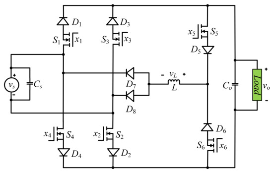
Figure 1.
Proposed circuit.
There is the use of six transistor-diode pairs S1-D1 to S6-D6. There is the additional use of two more diodes D7 and D8 that become forward-biased during the periods in which the input voltage (vs) is positive and negative, respectively. This arrangement of the switching devices avoids the possible short circuit loops formed due to the input capacitor (Cs) and output capacitor (Co) or their parallel connection. The role of these capacitors is to filter the ripple in the input and output voltage. The inductor (L) connected at the intermediate circuit stage is responsible for the storage and transfer of the input power. The direction of this inductor is always unidirectional, which is one of the attractive features of the circuit and eliminates the chance of sudden change or reversal of its current. Let us consider the worst-case switching interval in which all the six transistors are on. This event may be caused by some internal defect in the fabrication process of the switching transistors or programming errors in the control inputs. In this case, the anode voltage of diodes D1 and D4, D2 and D3, and D7 and D8 have equal anode voltage, but their cathode voltages are unequal. In the same way, the cathodes of the diodes D5 and D6 are connected to the same point having equal voltage at their cathodes and unequal voltage at their anodes. These pairs of diodes cannot conduct at the same time. So, there exist no short circuit loops for the input capacitor, output capacitor, or parallel connection. In this circuit, the problem of shoot-through is eliminated inherently.
The input voltage has two half cycles, and there are four possible ways to regulate and control these half cycles at the output. That includes the non-inverted and inverted forms both for the positive and negative half cycles of the input voltage. The regulation in the output can be step up (boost) and step down (buck). In this regard, the control inputs for voltage regulation are shown in Figure 2a,b to produce the voltage buck and boost operation.
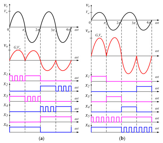
Figure 2.
High and low-frequency gating signals for (a) voltage buck operation and (b) voltage boost operation.
For the voltage buck operation, the peak magnitude of the output voltage is always less than the peak magnitude of the input voltage. The peak magnitude of the input is constant, but the peak magnitude of the output voltage is controllable through the regulation of duty cycle control. The high-frequency PWM control signals x1 and x3 with low-frequency control signal x6 are responsible for generating the positive pulses at the output. There is no role for the remaining signals (x2, x4,, and x5) for this operation. There is the use of high-frequency control signals x2, x4, and one low-frequency control signal x5 to generate negative output pulses at the output. A complete control scheme for the operation where the output frequency is half of the input frequency is shown in Figure 2a. For voltage boost operation, the high-frequency operation of the switching transistors is performed with the control signals x5 and x6. The generation of a group of positive and negative pulses is ensured at the output with the low-frequency operating transistors. The generation of control inputs x1 and x3 help to arrange the positive pulses at the output during the positive and negative half cycle of the input voltage, respectively. In the same way, control signals x4 and x2 are set to logic high for positive and negative input voltage, respectively. The PWM modulation of the high-frequency signals controls the gain (GV) of the converter.
2.1. Generation of Non-Inverted and Inverted Voltage Buck Outputs
The regulation in the load voltage (vo) can be confirmed via the duty cycle or PWM control (d1) developed for the operating transistors. In the voltage buck operation, the variation in the load voltage is ensured from the maximum value of the input voltage to some lower value. In this operation, the input power is sent to output via an intermediate inductor by turning on all transistors in that conducting loop. This process is continued for the on-time interval (d1T) of the one-control period (T). In the off-time interval ((1 − d1)T) of the switching period, the source voltage is removed from the circuit, and power stored in the inductor to now transferred to the load. Voltage buck operation in its non-inverted and inverted form for the positive and negative input voltage is detailed here.
The control signals in Figure 2a help to perform the voltage buck operation. Here the output is non-inverted for the first and fourth half cycles of the input voltage. The output voltage is positive in the first half cycle of the input voltage. To produce this output during this period, the switching transistor S1 operates with high-frequency PWM control while the transistors S3 and S6 remain on until the polarity of the input voltage is changed. The series-connected diode D3 with transistor S3 is reverse-biased as its cathode is connected with the positive terminal of the source voltage once the transistor S1 is on. No current can be conducted through this branch or pair. During this interval, the load is connected with the input as shown in the highlighted loop of Figure 3a as transistors S1 and S6 are on with the forward biasing of diodes D1, D6,, and D8. The value of voltage across the inductor (L) is detected in Equation (1) by applying the KVL in the existing loop.
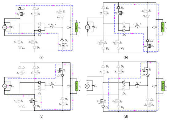
Figure 3.
Equivalent current-conducting loops with respect to input voltage to produce non-inverting buck operation during; (a,b) positive half cycles; (c,d) negative half cycles.
The continuity in the inductor current is granted with the turning on of the diode D3 once the high-frequency operating transistor S1 turns off. In this period ((1 − d1) T), the energy stored in the inductor is linked to the output with the highlighted loop in Figure 3b. In this interval, the inductor becomes a current source for the output and its voltage is founded through KVK analysis as
Next, the non-inverting voltage buck operation is considered for negative input voltage. The output of this mode is produced with the help of the high-frequency switching operation of the transistors S2 and S4. The switch S5 remains on for the period in which input voltage is negative to facilitate the conduction of continuous inductor and load currents. The current conduction loops in which the input power is stored and then transferred to the output is shown in Figure 3c,d. Here the transistors S2 and S4 operate in a complementary way. The high-frequency operation of the transistor S4 is controlled with the forward biasing and reversing of the diode D4. The operating behavior of this diode is directly linked with the operation of the transistor S2. There is no change in the value of the inductor voltage during the high-frequency on and off intervals as shown below.
The use of a high switching frequency facilitates considering the inductor voltage constant during one switching period. The balancing of the inductor volt-second principle helps to determine the voltage transfer ratio or voltage gain in terms of duty cycle control.
So
For the inverting voltage buck operation, the polarity of the output voltage is always inverted with respect to the input voltage. The inverted outputs are observed in the second and third half cycles of Figure 2a for negative and positive input voltage, respectively. A previous approach may be employed for validation of the inverting voltage gain. This includes the current conduction loops for power transfer and the value of the inductor voltage once it stores and releases the power toward the load. These loops are demonstrated in Figure 4a,b for positive input, and in Figure 4c,d for negative input voltage. The value of the inductor voltage can be simply modified from Equations (1) and (2) by just inverting the polarity of the output voltages and may be observed from Equations (8) and (9).
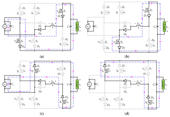
Figure 4.
Equivalent current-conducting loops with respect to the input voltage to produce inverting buck operation during; (a,b) positive half cycles; (c,d) negative half cycles.
By considering the principle of volt-second behavior of the inductor for one switching period, it may be noticed as:
The final closed forms of Equations (7) and (12) express the non-inverted and inverted relationship between the input and output voltage, respectively. The controllability of the output voltage can be governed with the help of duty cycle control. This arrangement ensures the voltage regulation in the instantaneous output voltage from maximum input voltage to some lower values.
It is investigated that in all equivalent current loops, there is the conduction of two transistors with their internal resistances rt, three diodes with their internal resistances rd, and there is one inductor with its resistance of rL. Therefore, the total resistance faced by the current conduction in these loops due to conducting devices and a filtering inductor can be calculated by adding their values. It can be seen as
The state space modeling of the voltage buck operation with duty cycle control of d1 for any polarity of the input voltage based on the PWM averaging principle as reported in [40] is formulated in Equations (14) and (15) for non-inverting and inverting operation, respectively. Here inductor current (iind(t)) and output capacitor voltage (vo(t)) are chosen as the state variable.
2.2. Generation of Non-Inverted and Inverted Voltage Boost Outputs
This operation is utilized for the application where the required instantaneous output voltage is greater than the input voltage. The required voltage gain is more than unity, and this is controllable with the help of the duty cycle control (d2) of high-frequency switching devices, especially transistors. The voltage boost operation comprises the first storage of the input power in the inductor. At that time, the load is completely isolated from the input source voltage, and power consumed by the load is supplied from the output capacitor. For this purpose, the size of this capacitor should be reasonable to lower the ripple in the output voltage and supply power to the load in this period. The period (that is, the known turn-on interval of a PWM control signal) in which the inductor is energized from the source voltage is directly linked with the amount of the required voltage gain. The value of the inductor voltage depends on this period. The load voltage is the sum of the input and inductor voltage in the turn-off interval of the PWM control signal. Surely this sum of the voltages is greater than the input voltage, so this operation is called a voltage boost operation. The only difference between the non-inverting and inverting processes is output voltage polarity with respect to the input voltage. The output voltage form is non-inverted and inverted if it is in-phase and out of phase with respect to the input voltage. This behavior of the output is explained in the next paragraphs.
Non-inverted and inverted voltage forms can be explained with respect to control inputs plotted in Figure 2b. Here it may notice that there are only two high-frequency control signals x5 and x6. The non-inverted and inverted versions of the input voltage are determined from the generation of the low-frequency signals. For example, to realize the non-inverted version of the input voltage, the low-frequency control inputs x1 and x2 are set to logic high during the intervals in which the input voltage has positive and negative half cycles, respectively. The current conducting loops for this process are highlighted in Figure 5a–d for positive and negative input voltage, respectively.
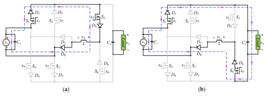
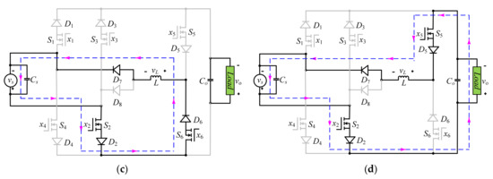
Figure 5.
Equivalent current-conducting loops with respect to the input voltage to produce non-inverting boost operation during; (a,b) positive half cycles; (c,d) negative half cycles.
The plots in Figure 5a,c show the current flowing paths to transform the input power to the inductor. In this process, the inductor voltage is equal to the input voltage as it is directly connected across the source voltage.
The output voltage is the sum of the input and inductor voltages once one high-frequency PWM control transistor turns off and the other turns on to keep the continuity of the inductor current. This behavior is highlighted in the plot of Figure 5b,d for positive and negative input voltage, respectively. During these intervals, the inductor voltage is the difference between input and output voltages, as can be viewed from Equation (17).
The voltage-second balance of the inductor voltage during the turn-on and off intervals helps to determine the voltage transfer ratio in terms of duty cycle control.
Similar control signals as shown in Figure 2b can be practiced to get the inverted version of the input voltage. To achieve this target, the role of x1 and x2 is exchanged with x3 and x4. The behavior of the high-frequency control signals remains unaltered as it is seen for a non-inverting operation. The plots of Figure 6a–d express the inverting boost operation for positive and negative input voltage, respectively. Parts ‘a’ and ‘c’ of this figure show the current conduction path that is used to transform the power from the input source to the intermediate inductor (L). The same inductor voltages as seen for a non-inverting operation can be observed in Equation (20) by using the KVL concept in the loops of Figure 6a,c.
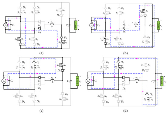
Figure 6.
Equivalent current-conducting loops with respect to the input voltage to produce inverting boost operation during: (a,b) positive half cycles; (c,d) negative half cycles.
Equation (20) can easily be obtained by inverting the polarity of the output voltage in Equation (17). This value of the inductor voltage can also be confirmed from the highlighted loops in Figure 6b,d. These current-conducting loops show how the stored energy is recovered and sent to the output using high-frequency PWM control.
The knowledge of the inductor volt-sec product leads to the development of the following voltage transfer ratio. This equation validates the inverted voltage response of the converter with voltage step-up features.
The observation of Equations (19) and (22) confirms the voltage step-up behavior. The output voltage may be a non-inverted or inverted version of the input voltage, and adjustment in the output can be attained by applying PWM control.
The state space modeling of the voltage boost operation with duty cycle control of d2 for both polarities of the input voltage that is based on the PWM averaging principle as discussed in [41] is formulated in Equations (23) and (24) for non-inverting and inverting operation, respectively.
The state space modeling of voltage buck and boost operation can also be merged into a single model, as may be seen from Equations (25) and (26) for non-inverting and inverting outputs, respectively.
The state space form shown in the above two equations represents the complete behavior of all operating modes in Figure 3, Figure 4, Figure 5 and Figure 6. Equations (25) and (26), respectively, show their non-inverting and inverting behavior. For example, for non-inverting buck operation for positive input voltage, the value of d2 is kept at zero. This value ensures that the transistor S5 is kept off all the time for the above operation (see Figure 3a,b). The duty cycle control of d1 is a PWM control that regulates the output voltage per requirements. In the same way, for boost operation, the value d1 is set to ‘1’, and now duty cycle control of d2 is a PWM control that controls the output voltage. Equation (25) represent Equations (14) and (23) by putting d2 = 0 and d1 =1, respectively. These values of the duty cycle control also help to converge Equation (26) to Equations (15) and (24), respectively. The developed steady-state representation may be used to find stability by designing an appropriate feedback controller.
3. Comparison and Analysis
The major achievement of the proposed circuit arrangement is a reduction in the switching devices. In the suggested circuit, there is the ability to govern the load voltage with the adjustment of the duty cycle, which is PWM control. The polarity of the output voltage can also be set to a positive or negative value for any polarity of the input voltage. The control in the output voltage can be settled to the required value by setting the positive and negative half cycles for the consecutive half periods of the output voltage. All these processes can be performed with the help of only six transistors and a diode. In the same way, the similar output in the existing converters uses eight transistors and diodes [28,39]. The use of gate control circuits is a fundamental need for the operating principle of switching transistors, and they require more space and have high costs. These circuits acquire a reasonable space in the total space of the switching converters. The compared parameters are listed in Table 1. The peak or rms voltage of the switching devices depends on the inductor value equal to the output and input currents for voltage buck and boost operations, respectively. In this regard, the switching voltages and currents of the proposed circuit and the existing converter [28,39] are the same. In the proposed circuit and converter in [28], there is only one energy-storing inductor and its current direction is unidirectional, which is one of the attractive features that limit the current interruption problem of the inductor current. This feature of the inductor current also helps to simplify the feedback control schemes. However, the converter of [39] has to use two energy-storing inductors. The inductor is connected to the input store and releases the energy to obtain voltage boost operation. The current flow in this inductor is bidirectional and there is no current interruption or reversal problem. However, the inductor connected toward the load side used to perform the voltage buck operation has a risk of reversal and interruption of its current. During the one operating cycle of the input voltage, there is the use of four low-frequency transistors and diodes in the proposed circuit and converter in [28,39]. These converters have equal conduction losses as listed in Table 1. In these computations, Vfd is the forward voltage of the diodes, and Rfd and Rtr are conducting resistances of the diodes and transistors, respectively. The converter in [39] only needs the high-frequency operations of the two transistors, so its switching losses are low, but these losses cannot significantly increase the overall conversion losses. Switching losses depend on the rise (tr) and fall (tf) times of the switching transistors, and their values in the modern age lie in the nanosecond range. The proposed topology simplifies the constraints of the existing circuits and increases the effectiveness or potency of application in various industrial drives.

Table 1.
Comparison with existing circuit topologies.
4. Results and Discussion
To examine the performance and operational features of the proposed circuit, various test platforms are employed, including the simulation approach and practical results obtained from real circuits. In this section, one output frequency is chosen to test the regulation in the voltage and inverted or non-inverted output with respect to a given source voltage. In these test results, the magnitude (180 V) and frequency (50 Hz) of the input voltage are kept constant. The frequency and magnitude of the load are regulated through switching signals. The low-frequency switching signals adjust the load frequency in some selected discrete steps, for example, one-half or one-third of the constant input frequency. On the other hand, the high-frequency PWM or duty cycle control governs the variation in the magnitude of the output voltage. For any required output frequency value, Table 2 shows the required value of the duty ratio control to obtain the peak output voltage of 50 V, 80 V, and 200 V from an input peak voltage of 180 V.
Table 2.
Required voltage gain or duty cycle ratio to obtain the required output.
The variation in the output voltage may be adjusted to any required value below 180 V and above 180 V with the proper setting of the duty ratio control.
4.1. Simulated Results
One of the attractive approaches is to test the outputs of the proposed circuit on a computer simulation before it is moved toward practical implementation. It is simple and easy to analyze the switching converters in this environment because there is no need for detecting or sensing the polarity of the input voltage. In this effort, the values of the designed components for practical realization are used to test the outputs. The modeling of the switching devices is developed with respect to the internal parameters of the transistors and diodes that are designed for practical setup. The role of the microcontroller is modeled by employing the pulse generators. A load of 100 Ω is connected to the output as a load to test its outputs. The purpose of this environment is to test the non-inverted and inverted voltage buck and boost operation with voltage regulation capabilities. For this purpose, the input peak voltage of 180 V is converted to 50 V and 100 V peak voltage, ensuring a voltage gain of 0.28 and 0.55, respectively, for voltage buck operation. The simulated output with these required values is plotted in Figure 7a,b.
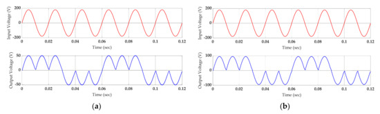
Figure 7.
Simulation results for output frequency step-down process with a voltage gain of (a) 0.28; (b) 0.55.
The output frequency of the output voltage is lowered to three times the input frequency. The voltage boost operation is also explored at the same frequency, and its output is presented in Figure 8 in simulation form.
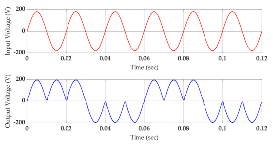
Figure 8.
Simulation results for output frequency step-down process with a voltage gain of 1.12.
These test results prove the required operation of the proposed converter. The observation of these figures indicates that the output voltage is a regulated form of the input voltage. This output can be converted into the non-inverted and inverted versions of the input voltage. These features of the output voltage enable variation in the load frequency to govern the output speed of the single-phase induction motors. For this purpose, a 180 W single-phase capacitor start induction motor is connected to the output as a load. The output speed variation of this motor is observed at three frequencies (50, 25, and 17 Hz) with various output voltage levels. The values of the input frequency and peak voltage are 50 Hz and 180 V, respectively. The values of the peak output voltage for these output frequencies are adjusted to 50 V and 80 V with the settings of duty ratio control of 0.28 and 0.55, respectively. Figure 9 shows the variation in the speed of the single-phase induction motor with respect to the variation in its voltage and frequency.
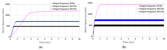
Figure 9.
Simulation results for motor output speed for various output frequencies with a voltage gain of (a) 0.28 and (b) 0.55.
It is observed that for 50 Hz frequency operation, there is no change in the output frequency with respect to input; the waveform quality of the output voltage is almost similar to the input voltage. There is a low ripple in its speed at this frequency compared to the 25 Hz and 17 Hz output frequencies. The variable frequency outputs always contain harmonics, which are investigated in [28,30]. Most of the effects of these harmonics are tackled by the inductance of the motor winding but there is a generation of some ripples in its output speed. The speed of the induction motor inversely varies with respect to the frequency, which means that at low frequencies, the motor speed is low, and it is high at higher frequencies. The variation in the speed is also directly proportional to the magnitude of the supplied voltage.
4.2. Practical Results
This section aims to convert the constant magnitude and frequency sinusoidal input (grid) voltage into various forms, that is, its non-inverting and inverting shapes with controllable magnitude and frequency. Some distortion may be added to the input voltage due to high switching frequency operation; one low-value capacitor (1 µF) can be connected to the input side. In the successful operation of the switching converters, there is always a need for an energy-storing inductor. In this regard, an inductor of 1 mH is used. The role of this inductor is to store and transfer the input energy to output with the high-frequency operation of the switching devices. The value of this inductor and switching frequency determines the amount of ripple in its current. The ripples and power quality directories of the output voltage also require the use of one output capacitor (4.7 µF). The photograph of this practical setup is shown in Figure 10. On the right side of this figure, six isolated DC supplies and six gate drivers are shown in two vertical rows. The RHRG3040 and IRF840 are used as high-frequency diodes and transistors, respectively. The EXB840 hybrid chip is used in the gate control circuit to increase the voltage level of the generated signal generator. Normally, the voltage level of the control signals lies in the range of 0 V to 5 V, but the required voltage value for the effective operation of the transistor IRF 840 may exceed 20 V. All the control signals generated by the micro-controller have the same reference voltage level. However, in switching converters, the voltage reference level of all control inputs should be isolated. This needs the isolated DC value of 20 V. For this purpose, a stepdown transformer in each isolated DC power supply ensures the required DC voltage and the electrical isolation between all outputs of the DC power supplies. The output of the microcontroller is supplied to the gate control circuit to isolate the reference points of all control signals and to set their magnitude to the required 20 V level. A voltage-detecting circuit is also required to determine the polarity of the input voltage. The output of this circuit ensures the alignment of all control signals with respect to the input voltage, having a peak voltage of 180 V.
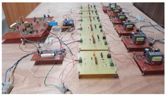
Figure 10.
Practical test circuit.
The inverted and non-inverted arrangement of the voltage buck and boost operation with various output voltages are shown in Figure 11 and Figure 12, respectively. These outputs are the recorded forms obtained from the Rigol oscilloscope. The input and output voltage waveforms of figures are represented with red and blue colors for their differentiation. Two cycles of the output voltage during the six cycles of the input voltage are investigated from these waveforms. One period of the output voltage contains three periods of the input voltage, so the output frequencies of these waveforms are one-third the frequency of the input voltage. It is also observed that during one period of the output, four pulses (first, third, fourth, and sixth) are in the non-inverted form of the input voltage while two pulses (second and fifth) are present in the inverted form of the input voltage. For the results of voltage buck operation as demonstrated in Figure 11a,b, the voltage gains of the power converting system are 0.3 and 0.55, as the peak values of these pulses are approximately 60 V and 100 V, respectively. The output of Figure 12 shows the voltage of the boost operation with the peak value of the output voltage at approximately 200 V. The results show in these waveforms that output voltage and frequency can be effectively produced with simple control schemes.
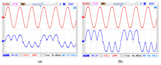
Figure 11.
Real value results for output frequency step-down process with a voltage gain of (a) 0.3 and (b) 0.55.
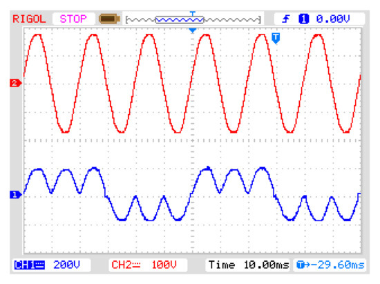
Figure 12.
Real value results for output frequency step-down process with a voltage gain of 1.12.
5. Conclusions
The present research is related to developing a compact-sized AC–AC converter that can produce controllable output in non-inverted and inverted voltage buck and boost forms. The value of the output can be set to any desired value with the PWM control. These output voltage features are used to obtain the required variable output frequency with the proper arrangement of positive and negative pulses. The independent voltage buck and boost operation enhance the controllability and flexibility through PWM control. This operation ensures low values of the voltage and current stresses for the components and semiconductor devices. There are also low values of the peak ripple currents and voltage; smooth variations in output voltage, output current, and input current are the main factors of the improved power quality. The regulation in the output voltage and frequency is obtained just by using six transistors and six diodes as compared to eight transistors and eight diodes in existing converters. The reduction in semiconductor devices lowers the size, losses, and overall cost. The major achievement in these values is due to the elimination of two transistors, as the size and cost of their control circuit are much larger with respect to their cost and size. There is also the use of only one filtering inductor and two filtering capacitors. The direction of this current is ensured to be continuous and unidirectional to tackle its interruption and reversal problem. Otherwise, there is a chance for the induction of high inductive voltage kicks, which may require complex switching arrangements. The details of all operating modes are highlighted indicating the non-inverting and inverting voltage operation both for the positive and negative input values. The proposed topology can vary the output frequency in step-down and step-up modes, so this can be effectively operated with unity and non-unity power factor loads. The simulation environment and practical setup circuit are developed to test its output for variable frequency operation with controllable voltage capabilities. These results confirm the usefulness of the developed circuit.
Author Contributions
Conceptualization, N.A. and G.A.; data curation, G.A. and N.U.; formal analysis, N.A. and M.E.F.; funding acquisition, N.U. and A.M.; investigation, N.A. and A.R.; methodology, G.A. and A.M.; project administration, G.A.; resources, M.E.F. and N.U.; software, A.R.; validation, G.A. and A.R.; writing—original draft, N.A. and G.A.; writing—review and editing, G.A., M.E.F., A.M., and N.U. All authors have read and agreed to the published version of the manuscript.
Funding
This research work is supported by Taif University Researchers Supporting Project Number TURSP-2020/144, Taif University, Taif, Saudi Arabia.
Institutional Review Board Statement
Not applicable.
Informed Consent Statement
Not applicable.
Data Availability Statement
Not applicable.
Acknowledgments
The authors acknowledge the financial support from Taif University Researchers Supporting Project Number TURSP-2020/144, Taif University, Saudi Arabia. The authors are also thankful to the Department of Electrical Engineering, the University of Lahore, Pakistan for providing the facilities to conduct this research.
Conflicts of Interest
The authors declare no conflict of interest.
References
- Abdoli, I.; Mosallanejad, A. A highly efficient isolated single-phase variable frequency AC–AC converter with flexible buck-boost factor, inherent safe commutation, and continuous current. IET Power Electron. 2022. [Google Scholar] [CrossRef]
- Barrera-Cardenas, R.; Molinas, M. Comparative Study of Wind Turbine Power Converters Based on Medium-Frequency AC-Link for Offshore DC-Grids. IEEE J. Emerg. Sel. Top. Power Electron. 2015, 3, 525–541. [Google Scholar] [CrossRef]
- Subramanian, S.; Mishra, M.K. Interphase AC–AC Topology for Voltage Sag Supporter. IEEE Trans. Power Electron. 2010, 25, 514–518. [Google Scholar] [CrossRef]
- Zheng, Z.; Xiao, X.; Chen, X.; Huang, C.; Zhao, L.; Li, C. Performance Evaluation of a MW-Class SMES-BES DVR System for Mitigation of Voltage Quality Disturbances. IEEE Trans. Ind. Appl. 2018, 54, 3090–3099. [Google Scholar] [CrossRef]
- Roldán-Pérez, J.; García-Cerrada, A.; Ochoa-Giménez, M.; Zamora-Macho, J.L. Delayed-Signal-Cancellation-Based Sag Detector for a Dynamic Voltage Restorer in Distorted Grids. IEEE Trans. Sustain. Energy 2019, 10, 2015–2027. [Google Scholar] [CrossRef]
- Biricik, S.; Komurcugil, H.; Ahmed, H.; Babaei, E. Super Twisting Sliding-Mode Control of DVR With Frequency-Adaptive Brockett Oscillator. IEEE Trans. Ind. Electron. 2021, 68, 10730–10739. [Google Scholar] [CrossRef]
- Jothibasu, S.; Mishra, M.K. An Improved Direct AC–AC Converter for Voltage Sag Mitigation. IEEE Trans. Ind. Electron. 2015, 62, 21–29. [Google Scholar] [CrossRef]
- Lodetti, S.; Azcarate, I.; Gutiérrez, J.J.; Leturiondo, L.A.; Redondo, K.; Sáiz, P.; Melero, J.J.; Bruna, J. Flicker of modern lighting technologies due to rapid voltage changes. Energies 2019, 12, 865. [Google Scholar] [CrossRef]
- Kaniewski, J.; Szczesniak, P.; Jarnut, M.; Benysek, G. Hybrid Voltage Sag\/Swell Compensators: A Review of Hybrid AC\/AC Converters. IEEE Ind. Electron. Mag. 2015, 9, 37–48. [Google Scholar] [CrossRef]
- Moghassemi, A.; Padmanaban, S.K. Dynamic voltage restorer (DVR): A comprehensive review of topologies, power converters, control methods, and modified configurations. Energies 2020, 13, 4152. [Google Scholar] [CrossRef]
- Khan, U.A.; Khan, A.A.; Cha, H.; Kim, H.; Kim, J.; Baek, J. Dual-Buck AC–AC Converter with Inverting and Non-Inverting Operations. IEEE Trans. Power Electron. 2018, 33, 9432–9443. [Google Scholar] [CrossRef]
- Sharifi, S.; Monfared, M.; Nikbahar, A. Highly Efficient Single-Phase Direct AC-to-AC Converter with Reduced Semiconductor Count. IEEE Trans. Ind. Electron. 2021, 68, 1130–1138. [Google Scholar] [CrossRef]
- Ran, X.; Xu, B.; Liu, K.; Zhang, J. An Improved Low-Complexity Model Predictive Direct Power Control with Reduced Power Ripples Under Unbalanced Grid Conditions. IEEE Trans. Power Electron. 2022, 37, 5224–5234. [Google Scholar] [CrossRef]
- Kolar, J.W.; Friedli, T.; Rodriguez, J.; Wheeler, P.W. Review of Three-Phase PWM AC–AC Converter Topologies. IEEE Trans. Ind. Electron. 2011, 58, 4988–5006. [Google Scholar] [CrossRef]
- Petrauskas, G.; Svinkunas, G. Application of Single-Phase Supply AC-DC-AC VFD for Power Factor Improvement in LED Lighting Devices Loaded Power Distribution Lines. Appl. Sci. 2022, 12, 5955. [Google Scholar] [CrossRef]
- Liu, X.; Loh, P.C.; Wang, P.; Han, X. Improved Modulation Schemes for Indirect Z-source Matrix Converter With Sinusoidal Input and Output Waveforms. IEEE Trans. Power Electron. 2012, 27, 4039–4050. [Google Scholar] [CrossRef]
- Wang, H.; Wang, H.; Zhu, G.; Blaabjerg, F. An Overview of Capacitive DC-Links-Topology Derivation and Scalability Analysis. IEEE Trans. Power Electron. 2020, 35, 1805–1829. [Google Scholar] [CrossRef]
- Zhao, Z.; Davari, P.; Lu, W.; Wang, H.; Blaabjerg, F. An Overview of Condition Monitoring Techniques for Capacitors in DC-Link Applications. IEEE Trans. Power Electron. 2021, 36, 3692–3716. [Google Scholar] [CrossRef]
- De Freitas, N.B.; Jacobina, C.B.; Cunha, M.F. Multilevel Single-Phase Converter with Two DC Links. IEEE Trans. Ind. Electron. 2020, 67, 10346–10355. [Google Scholar] [CrossRef]
- De Lacerda, R.P.; Jacobina, C.B.; Fabricio, E.L.L.; Rodrigues, P.L.S. Six-Leg Single-Phase AC–DC–AC Multilevel Converter With Transformers for UPS and UPQC Applications. IEEE Trans. Ind. Appl. 2020, 56, 5170–5181. [Google Scholar] [CrossRef]
- Rde Lacerda, P.; Jacobina, C.B.; Fabricio, E.L.L. Single-Phase AC–DC–AC Multilevel Converter Based on Parallel-/Series-Connected Three-Leg Modules. IEEE Trans. Ind. Appl. 2022, 58, 3706–3720. [Google Scholar] [CrossRef]
- Banaei, M.R.; Alizadeh, R.; Jahanyari, N.; Najmi, E.S. An AC Z-Source Converter Based on Gamma Structure with Safe-Commutation Strategy. IEEE Trans. Power Electron. 2016, 31, 1255–1262. [Google Scholar] [CrossRef]
- Vidhya, D.S.; Venkatesan, T. Quasi-Z-Source Indirect Matrix Converter Fed Induction Motor Drive for Flow Control of Dye in Paper Mill. IEEE Trans. Power Electron. 2018, 33, 1476–1486. [Google Scholar] [CrossRef]
- Bozorgi, A.M.; Hakemi, A.; Farasat, M.; Monfared, M. Modulation Techniques for Common-Mode Voltage Reduction in the Z-Source Ultra Sparse Matrix Converters. IEEE Trans. Power Electron. 2019, 34, 958–970. [Google Scholar] [CrossRef]
- Li, P.; Hu, Y. Unified Non-Inverting and Inverting PWM AC–AC Converter with Versatile Modes of Operation. IEEE Trans. Ind. Electron. 2017, 64, 1137–1147. [Google Scholar] [CrossRef]
- Ahmed, H.F.; el Moursi, M.S.; Cha, H.; al Hosani, K.; Zahawi, B. A Reliable Single-Phase Bipolar Buck–Boost Direct PWM AC–AC Converter With Continuous Input/Output Currents. IEEE Trans. Ind. Electron. 2020, 67, 10253–10265. [Google Scholar] [CrossRef]
- He, L.; Xu, X. Novel High-Efficiency Frequency-Variable Buck–Boost AC–AC Converter with Safe-Commutation and Continuous Current. IEEE Trans. Power Electron. 2020, 35, 13225–13238. [Google Scholar] [CrossRef]
- Ashraf, N.; Izhar, T.; Abbas, G.; Balas, V.E.; Balas, M.M.; Lin, T.C.; Asad, M.U.; Farooq, U.; Gu, J. A Single-Phase Buck and Boost AC-to-AC Converter with Bipolar Voltage Gain: Analysis, Design, and Implementation. Energies 2019, 12, 1376. [Google Scholar] [CrossRef]
- Ashraf, N.; Abbas, G.; Abbassi, R.; Jerbi, H. Power quality analysis of the output voltage of AC voltage and frequency controllers realized with various voltage control techniques. Appl. Sci. 2021, 11, 538. [Google Scholar] [CrossRef]
- Ashraf, N.; Abbas, G.; Ullah, N.; Al-Ahmadi, A.A.; Raza, A.; Farooq, U.; Jamil, M. Investigation of the Power Quality Concerns of Input Current in Single-Phase Frequency Step-Down Converter. Appl. Sci. 2022, 12, 3663. [Google Scholar] [CrossRef]
- Kumar, A.; Sadhu, P.K.; Mohanta, D.K.; Reddy, M.J.B. An effective switching algorithm for single phase matrix converter in induction heating applications. Electronics 2018, 7, 149. [Google Scholar] [CrossRef]
- Mondol, M.H.; Uddin, M.S.; Hossain, E.; Biswas, S.P. A Compact and Cost Efficient Multiconverter for Multipurpose Applications. IEEE Access 2020, 8, 86810–86823. [Google Scholar] [CrossRef]
- Ashraf, N.; Abbas, G.; Khan, I.; Raza, A.; Ullah, N. A Transformer-Less Multiconverter Having Output Voltage and Frequency Regulation Characteristics, Employed with Simple Switching Algorithms. Appl. Sci. 2021, 11, 3075. [Google Scholar] [CrossRef]
- Fayek, T.I.H.H.; Rusu, E.; Rahman, F. Triac Based Novel Single Phase Step-Down Cycloconverter with Reduced THDs for Variable Speed Applications. Appl. Sci. 2021, 11, 8688. [Google Scholar]
- Uddin, M.; Biswas, S.P.; Islam, M.R.; Anower, M.S.; Kouzani, A.Z.; Mahmud, M.A. A new generalized step-down single-stage AC/AC power converter. Sustainability 2020, 12, 9181. [Google Scholar] [CrossRef]
- Ashraf, N.; Abbas, G.; Ullah, N.; Al-Ahmadi, A.A.; Yasin, A.R.; Awan, A.B.; Jamil, M. A Transformerless AC-AC Converter with Improved Power Quality Employed to Step-Down Power Frequency at Output. Energies 2022, 15, 667. [Google Scholar] [CrossRef]
- Zhang, S.; Wang, C.; Chen, D. A Single-Stage Wireless Power Transfer Converter with Hybrid Compensation Topology in AC Input. IEEE Trans. Veh. Technol. 2022, 71, 8266–8279. [Google Scholar] [CrossRef]
- Ahmed, H.F.; Cha, H.; Khan, A.A.; Kim, J.; Cho, J. A Single-Phase Buck–Boost Matrix Converter with Only Six Switches and Without Commutation Problem. IEEE Trans. Power Electron. 2017, 32, 1232–1244. [Google Scholar] [CrossRef]
- Ahmed, H.F.; el Moursi, M.S.; Zahawi, B.; Hosani, K.A. High-Efficiency Single-Phase Matrix Converter with Diverse Symmetric Bipolar Buck and Boost Operations. IEEE Trans. Power Electron. 2021, 36, 4300–4315. [Google Scholar] [CrossRef]
- Ashraf, N.; Izhar, T.; Abbas, G.; Awan, A.B.; Farooq, U.; Balas, V.E. A New Single-Phase AC Voltage Converter with Voltage Buck Characteristics for Grid Voltage Compensation. IEEE Access 2020, 8, 48886–48903. [Google Scholar] [CrossRef]
- Ashraf, N.; Abbas, G.; Ullah, N.; Alkhammash, H.I.; Zubair, M. An Improved Bipolar Voltage Boost AC Voltage Controller With Reduced Switching Transistors. IEEE Access 2021, 9, 90402–90417. [Google Scholar] [CrossRef]
Publisher’s Note: MDPI stays neutral with regard to jurisdictional claims in published maps and institutional affiliations. |
© 2022 by the authors. Licensee MDPI, Basel, Switzerland. This article is an open access article distributed under the terms and conditions of the Creative Commons Attribution (CC BY) license (https://creativecommons.org/licenses/by/4.0/).