


Nanomaterials for Optoelectronic Devices: Synthesis, Properties, and Applications
A special issue of Nanomaterials (ISSN 2079-4991). This special issue belongs to the section "Nanophotonics Materials and Devices".
Deadline for manuscript submissions: 10 July 2026 | Viewed by 4637
Special Issue Editor

Interests: two-dimensional materials; quantum sensing; excitonic dynamics; nanomaterials; thin films; optoelectronics; solar cells; energy harvesting; heterojunctions
Special Issue Information
Dear Colleagues,
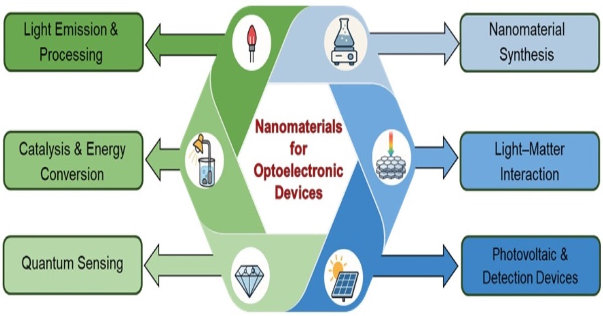
The rapid advancement of nanomaterials has opened new opportunities in optoelectronic technologies, enabling major improvements in efficiency, tunability, and integration. These developments have expanded the scope of devices such as photodetectors, solar cells, LEDs, lasers, and optical sensors.
This Special Issue, Nanomaterials for Optoelectronic Devices: Synthesis, Properties, and Applications, invites original research articles, review papers, theoretical studies, and perspectives on the synthesis, characterization, and application of advanced nanomaterials—including quantum dots, nanocrystals, 2D materials, and hybrid heterostructures—for modern optoelectronic systems.
We welcome submissions on scalable fabrication techniques (e.g., solution processing, PVD, CVD, ALD), surface and interface engineering, charge transport, exciton dynamics, and light–matter interaction. Studies addressing challenges such as long-term stability, eco-friendly processing, and large-scale integration are strongly encouraged.
In addition to traditional optoelectronic applications, we also invite work on light-driven photocatalysis, photoelectrochemical systems, bio-integrated optoelectronics, neuromorphic devices, and nanophotonics for quantum sensing and communication.
This Special Issue aims to highlight innovative approaches that connect fundamental research with real-world device technologies. Contributions from a broad range of disciplines are encouraged to promote cross-cutting advances in nanomaterial-enabled optoelectronics.
We look forward to receiving your contributions.
Dr. Yusuf Selim Ocak
Guest Editor
Manuscript Submission Information
Manuscripts should be submitted online at www.mdpi.com by registering and logging in to this website. Once you are registered, click here to go to the submission form. Manuscripts can be submitted until the deadline. All submissions that pass pre-check are peer-reviewed. Accepted papers will be published continuously in the journal (as soon as accepted) and will be listed together on the special issue website. Research articles, review articles as well as short communications are invited. For planned papers, a title and short abstract (about 250 words) can be sent to the Editorial Office for assessment.
Submitted manuscripts should not have been published previously, nor be under consideration for publication elsewhere (except conference proceedings papers). All manuscripts are thoroughly refereed through a single-blind peer-review process. A guide for authors and other relevant information for submission of manuscripts is available on the Instructions for Authors page. Nanomaterials is an international peer-reviewed open access semimonthly journal published by MDPI.
Please visit the Instructions for Authors page before submitting a manuscript. The Article Processing Charge (APC) for publication in this open access journal is 2400 CHF (Swiss Francs). Submitted papers should be well formatted and use good English. Authors may use MDPI's English editing service prior to publication or during author revisions.
Keywords
- optoelectronic devices
- nanomaterial synthesis
- quantum nanostructures
- nanocrystals
- 2D materials
- hybrid and heterostructure materials
- photovoltaics
- photodetectors
- charge and exciton dynamics
- photocatalysis and PEC systems
- quantum sensing
- scalable fabrication
Benefits of Publishing in a Special Issue
- Ease of navigation: Grouping papers by topic helps scholars navigate broad scope journals more efficiently.
- Greater discoverability: Special Issues support the reach and impact of scientific research. Articles in Special Issues are more discoverable and cited more frequently.
- Expansion of research network: Special Issues facilitate connections among authors, fostering scientific collaborations.
- External promotion: Articles in Special Issues are often promoted through the journal's social media, increasing their visibility.
- Reprint: MDPI Books provides the opportunity to republish successful Special Issues in book format, both online and in print.
Further information on MDPI's Special Issue policies can be found here.