Abstract
Indium tin oxide (ITO) thin films are widely used as transparent electrodes in electronic devices. Many of those electronic devices are heat sensitive, thus their manufacturing process steps should not exceed 100 °C. Manufacturing competitive high-quality ITO films at low temperature at industrial scale is still a challenge. Magnetron sputtering technology is the most suitable technology fulfilling those requirements. However, ITO layer properties and the reproducibility of the process are extremely sensitive to process parameters. Here, morphological, structural, electrical, and optical characterization of the ITO layers deposited at low temperature has been successfully correlated to magnetron sputtering process parameters. It has been demonstrated that the oxygen flow controls and influences layer properties. For oxygen flow between 3–4 sccm, high quality crystalline layers were obtained with excellent optoelectronic properties (resistivity <8 × 10⁻⁴ Ω·cm and visible transmittance >80%). The optimized conditions were applied to successfully manufacture transparent ITO heaters on large area glass and polymeric components. When a low supply voltage (8 V) was applied to transparent heaters (THs), de-icing of the surface was produced in less than 2 min, showing uniform thermal distribution. In addition, both THs (glass and polycarbonate) showed a great stability when exposed to saline solution.
1. Introduction
Transparent conductive oxides (TCOs) have attracted wide interest due to their high optical transmittance in the visible wavelength region combined with high electrical conductivity. Due to these properties, they are extensively used as low emissivity layers in architectural glass or as transparent electrodes in multiple devices such as flat panel displays, electrochromic devices, photovoltaic cells, and organic light emitting diodes [,], or more recently, in microwave and radio frequency shielding devices []. In addition, TCO coatings can be applied as transparent heaters (THs) [] to fast and reliably heat glass and plastic components in the automotive, locomotive, and aircraft industries (in devices such as windscreens or car headlights) to provide them with de-fogging and/or de-icing properties within harsh environments, improving the performance of currently applied solutions. For example, contemporary car windshields are laminated with polyvinyl butyral (PVB) polymeric foils containing tungsten microwires as heating element. However, these types of heated windshields show a lack in the homogeneity of heat distribution over the windshield and in their transparency. Lenses in new automotive LED headlights also lead to issues with fogging or freezing because of the condensation occurring in the interior of the outer lens. Generally, the headlight housings have vent holes with filters to recirculate air and avoid condensation, of which the number and position must be frequently modified after headlight manufacturing to optimize air recirculation, in a difficult and expensive process []. This has become a challenging issue from a visibility and a safety standpoint for many original equipment manufacturers (OEMs). As in the case of windshields, microwires are also commonly used as heating elements, interfering with radio detection and ranging (RADAR) and light imaging detection and ranging (LIDAR) car systems. TCO coatings can improve the performance of conventional heating elements, in terms of demonstrating a high heating power capacity with fast control of temperature and small thermal inertia without detriment to their optical transmission [].
Indium tin oxide (ITO) is the most widely used TCO because it has unique set of properties; such as high ultraviolet absorption, high infrared reflectance, high microwave attenuation, wide bandgap (3.5–4.2 eV), high visible transmission, low electrical resistivity, good mechanical strength and abrasion resistance, chemical stability [] and compatibility with fine patterning processes []. There are many deposition techniques to obtain high quality ITO films, such as radio frequency (RF) [] and direct-current (DC) magnetron sputtering [], E-beam evaporation [], pulsed laser deposition (PLD) [], and spray pyrolysis []. Among all of them, pulsed DC magnetron sputtering is the most suitable to manufacture ITO layers at industrial scale due to the high deposition rate and quality control of the thin films [].
ITO layer properties are very dependent on sputtering process parameters such as temperature, pressure, target to subtract distance, discharge power and frequency, and oxygen and argon pressure during deposition, which are directly related to the physical nature of the films []. This physical nature encompasses structural characteristic, crystallinity, impurity levels (or doping), defect characteristics, uniformity, and stoichiometry. Thorough understanding of the relationship between sputtering process parameters, layer properties, and the physical nature of the layers is essential to obtain good reproducibility of the film properties, above all, at an industrial scale.
Many studies reporting on ITOs deposited by DC magnetron sputtering have shown that ITO thin films could reach high transparency in the visual region (90%) and high conduction properties (ρ = 2 × 10⁻⁴ Ω·cm). These optimal results are obtained at high substrate temperatures (>200 °C) during deposition or by post-annealing process afterwards, because temperature promotes crystallization of the layers and oxygen-vacancy creation, the main conduction mechanisms in ITO layers []. Many of those studies encompass the analysis of the relationship between process parameters and optoelectronic properties for high temperature ITO layers [,,,]. However, reaching high values of transmission and conductivity for ITO films at room temperature deposition is still a challenge for industrial reproducible magnetron sputtering processes. For room temperature sputtering deposition, oxygen flow effects on optical (average transmission in the visible light region, transmission and absorption spectra) and electrical (amount and mobility of electric carriers) features are two of the main factors affecting layer properties and have been previously studied, as well as effects on microstructure (grade of crystallinity, growth orientation, lattice parameter and lattice stress, grain size and structure), mainly for laboratory sputtering equipment [,,]. However, there is still a lack of understanding of the relationship of those parameters for pulsed DC magnetron sputtering industrial processes at room temperature. Although TCOs were applied as THs before 1995, they have been mainly studied in the framework of industrial research and development, and very few reports can be found in the literature about the application of ITO as THs [,]. In these reports, ITO nanoparticles were deposited on glass substrates by spin coating, producing ITO films with high transparency but high sheet resistances (above 300 Ω/sq) even after applying annealing at high temperatures.
In the present work, a detailed study of the influence of the oxygen flow on ITO layer properties has been performed for an unbalanced pulsed DC magnetron sputtering process at low temperature. The unbalance DC magnetron sputtering process is optimum for industrial applications because it presents higher deposition rates than the balance magnetron sputtering process. However, special attention must be given to avoid the bombardment of the growing film with ion species from the plasma (O2− in this case) that negatively affects the microstructure of the layers and damages the electrical properties []. The optimization of the ITO layer at room temperature has been performed for this unbalanced magnetron sputtering process for the deposition of ITO layers at semi-industrial scale. A detailed study including microstructure analysis of ITO film series deposited under different oxygen flows has been performed. Microstructure evolution with oxygen is explained and correlated with optoelectrical properties of each film. In addition, a cost-effective process was developed and optimized for the manufacturing of THs with excellent optoelectronic properties on large area glass and polycarbonate (PC) sheets by means of conventional sputtering at room temperature.
2. Materials and Methods
ITO layers have been deposited in an industrial pulsed DC unbalanced magnetron sputtering equipment, FASTCOAT, designed and manufactured by TEKNIKER (Eibar, Spain). This equipment has one unbalanced magnetron of 550 × 125 mm2 target size. The ITO (In2O3:Sn2O3 at. % 90:10 99.99% purity) target was placed 120 mm from a rotatable substrate holder. Two types of substrates were used for characterization purpose, silicon wafers and microscope glass slides (Menzel-Gläser). The ITO films were deposited at 1500 W average power, using an Advanced Energy DC Pinnacle Plus (Advance Energy, Denver, CO, USA) power supply, under the following pulsing parameters: 75 kHz pulse frequency, 4 µs pulse-off time, and a duty cycle of 70%. The vacuum chamber, which had a 230 L volume, was pumped down with a pumping speed of 1200 L/s to a base pressure of 2 × 10⁻⁶ mbar before the deposition. The gas entry supply was located closer to the substrate than to the target to avoid the acceleration of the oxygen ions by the potential applied to the target and, therefore, the bombardment of the growing film with O+ species from the plasma. During the deposition, argon flow was maintained constant at 150 sccm, while variable oxygen flow was introduced into the chamber by mass flow controllers, resulting in 1.8 × 10⁻³ mbar process pressure. Before deposition, the target was pre-sputtered for 10 min; the first 5 min with the same Ar flow of the process but without oxygen, and the last 5 min with both O2 and Ar flows applied during the process.
Oxygen flow was varied from 0 to 6 sccm, testing 7 different values, to correlate the oxygen flow influence with layer properties and morphology. The deposition rate of the layers was 20 nm/min (remaining unchanged for the different oxygen flow applied), obtaining 140 nm thick layers by depositing ITO for 7 min. Vacuum time and base pressure were kept constant for all the deposition processes performed at different oxygen flow, so the possible presence of residual impurities in the films caused by the gettering of water vapor from the chamber was the same.
The electrical properties were measured by 4-point probe [] and Hall Effect measurements (ECOPIA, Anyang City, South Korea). Optical transmittance was measured with a Perkin Elmer Lambda UV/VIS/NIR spectrophotometer (Perkin Elmer, Waltham, MA, USA). Morphology studies were made by an ULTRA Plus Carl-Zeiss field emission scanning electron microscope (FE SEM, Carl-Zeiss, Oberkochen, Germany) and an atomic force microscope Solver PRO NT-MDT (NT-MDT SI, Limerick, Ireland). The average surface roughness (Sa) and root mean square roughness (Sq) values have been calculated from 3 measurements of 3 × 3 µm2 AFM images of ITO layers deposited with different oxygen flows. A D8 Advance Bruker X-ray diffractometer (Bruker, Billerica, MA, USA) was used to determine the crystallinity of the films deposited on glass by measuring with Cu-Kα radiation in θ−2θ geometry with a step of 0.02°, a step time of 7.2 s, and applying a grazing incidence of 2° (GIXRD).
Glass and polycarbonate (PC) samples of 100 × 100 mm2 were used as prototypes of THs to evaluate their performance. Contacts were made by a conductor tape (tin-plated copper foil, PPI Adhesive Products Ltd.,Waterford, Ireland) to apply a DC voltage to the prototypes, and a thermographic camera was used to measure the temperature versus time to calculate the saturation temperatures at different applied voltages (2–12 V for standard uses). Temperature stability was also analyzed by applying a constant voltage (8 V) for 4 h. In addition, prototype de-fogging and de-icing properties were examined by measuring the time required to defog and/or defrost the samples after keeping them for 30 min in a refrigerator at −21 °C and applying a DC voltage of 8 V. Prototype durability was analyzed by applying adhesion tests using scotch tape (standard MIL-C-675C [] for the coating of glass optical elements).
3. Results
3.1. Effects of Oxygen Flow on the Morphology of ITO Thin Films
The effect of the oxygen flow on the morphology of the ITO layers is shown in Figure 1 (SEM images) and Figure 2 (AFM images). For low oxygen flows (0–1 sccm), the ITO surface was smooth (with surface roughness values around 0.8 nm) with no spikes and with a cauliflower-like microstructure. When oxygen flow increased (2–6 sccm), the surface became more granular, with greater surface roughness, and shaped crystallites appeared, increasing the number of polycrystalline grains with the oxygen flow. For an oxygen flow of 2–3 sccm, the cauliflower-like structure was mixed with crystalline grains. From 4 sccm and above, homogeneous polycrystalline surfaces were observed, with a significant increase in surface roughness (until 2 nm of Sa and 2.5–3 of Sq).
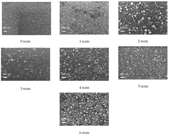
Figure 1.
SEM images of the surface of indium tin oxide (ITO) layers deposited with different oxygen flows.
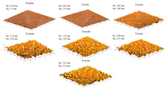
Figure 2.
2D and 3D AFM images of ITO layers surface. Average (Sa) and root mean square (Sq) roughness were calculated.
To correlate surface morphology with layer crystalline structure, XRD analysis was performed (Figure 3). XRD patterns showed that the oxygen flow affects the crystallinity of the layers. XRD pattern for the ITO deposited with 0 sccm of oxygen showed a halo pattern around 2θ = 32°–35°, which is characteristic of amorphous materials. For 1 sccm oxygen flow, a broad diffraction peak appeared around 2θ = 30°, corresponding to an incipient crystallization of the ITO layer in the (222)-oriented bcc structure of In2O3 []. Both results can be correlated with the SEM and AFM pictures of 0 and 1 sccm, where surface was smooth, and no grains were observed. When oxygen flow increased (2–5 sccm), the (222) diffraction peak became more intense and narrower, indicating the growth of the (222)-oriented crystallites, while new diffraction peaks appeared showing the formation of crystallites with other orientations. This correlates with the SEM (Figure 1) and AFM (Figure 2) surface images, where geometrically regular forms (scales and pyramidal peaks) fill the surface. However, a reduction in (222) peak intensity was observed when the oxygen flow was further increased up to 6 sccm A shift to higher angles was observed for the (222) peak when oxygen flow varied from 4 to 5 sccm. When increasing the oxygen flow from 1 sccm onwards, small diffraction peaks typical of polycrystalline ITO thin films with a cubic indium oxide structure appeared [], showing a minor formation of crystallites with other orientations such as (400), (332), (431), (440), and (622).
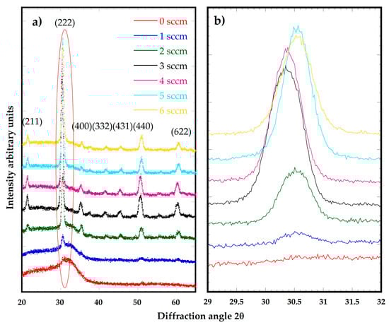
Figure 3.
XRD patterns of ITO deposited with an oxygen flow from 0 to 6 sccm: (a) measured in diffraction angle from 20 to 65; (b) Zoomed view of (222) peak.
Figure 4 shows the optical transmittance of each sample from the ultraviolet (λ = 250 nm) to the near-infrared (λ = 2500 nm) region. The mean transmission values in the visible region increased with the oxygen flow. Non-crystallized ITO layers (produced with 0 and 1 sccm of oxygen flows) had much lower average light transmission (around 65%) than crystallized layers produced with an O2 flow >3 sccm, which showed transmission values above 80% in the visible region, reaching the maximum value of 82% for 6 sccm.
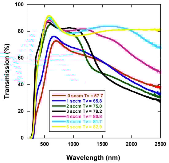
Figure 4.
Transmittance of ITO films sputtered with different oxygen flows. Mean transmittance values (Tv) for each oxygen flow are given.
In the near-infrared region (800–2500 nm), the behavior was different: first, the transmission decreased when the oxygen flow was increased from 0 to 3 sccm, whereas the opposite tendency was observed upon 4 sccm.
The evolution of electrical properties of the ITO layers, such as resistivity, carrier concentration, and Hall mobility with the oxygen flow is shown in Figure 5. We observed that the electrical properties were highly influenced by the oxygen flow applied during deposition of the ITO layer. Increasing the oxygen flow until 5 sccm boosted the Hall mobility to reach a maximum value of (36 ± 1) cm2/V·s. On the contrary, the increase in the oxygen flows led (from 0 to 2 sccm) to a slight enhancement of the carrier concentration with a subsequent reduction until reaching a minimum value below 1 × 1020 cm−3 at 6 sccm of oxygen flow. The resistivity seemed to be dominated by the Hall mobility, remaining at a minimum value of approximately 1 × 10⁻³ Ω·cm for hall mobility above 10 cm2/V·s. In this range, only a significant increase in resistivity was produced when the carrier concentration decreased below 1 × 1020 cm−3 at 6 sccm of oxygen flow. It is also worth highlighting that the sharpest decrease in resistivity was produced when the ITO layer was deposited in the presence of oxygen, with respect to those obtained in pure argon atmosphere.
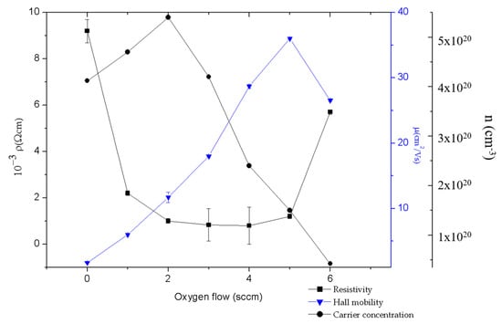
Figure 5.
Variation of carrier concentration (circular dots), carrier mobility (triangular dots), and resistivity (squared dots) of ITO layers deposited with and without different oxygen flows. If error bars are not visible, they are smaller than the symbol size.
3.2. Manufacturing of Transparent ITO Heaters
Table 1 summarizes the optoelectronic properties of the deposited ITO layers. In addition to the previously measured properties, the sheet resistance (measure of resistance on uniform thin films) and the Haacke’s figure of merit (FoM, a dimensionless parameter to evaluate the performance of thermoelectric materials) were also calculated because of their importance in many industrial applications of TCOs. FoM was calculated from the average optical transmittance at VIS region, and the sheet resistance (SR) []:

Table 1.
Average optical transmission in the visible region, T (%), Hall mobility (µ), carrier concentration (n), sheet resistance (SR), electrical resistivity (ρ), and FoM (ϕVIS) of ITO layers.
The ITO thin film showing optimal optoelectronic properties, in terms of reaching a commitment between transmission and conductivity, was the one deposited with an oxygen flow of 3 sccm, which showed the highest FoM (12.6 × 10⁻³ Ω−1). These conditions were applied on large-area glass and PC sheets of 100 mm2 for the manufacturing of transparent ITO heaters by a cost-effective process developed at room temperature. Electrical circuits were mounted on coated glass and PC samples to study heat transmission and evaluate the coating performance.
Figure 6 shows the saturation temperature of the selected ITO thin film deposited on glass (a) and PC (b) as a function of the applied power. The thermal resistance was calculated from the slope of the curve fit.
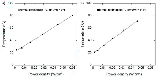
Figure 6.
Saturation temperature of ITO thin films deposited on glass (a) and PC (b) samples as a function of the applied power.
The times required to completely defrost the ITO coated glass and PC samples when applying a DC voltage of 8 V after keeping the samples in a refrigerator at −21 °C for 30 min were 2 and 1.5 min, respectively (Figure 7). The long-term working stability of the ITO thin film was proven by applying a constant voltage of 8 V for 4 h (Figure 8). Both samples did not show any sign of degradation after applying the adhesion tape test and after being immersed for 24 h in saline solution.
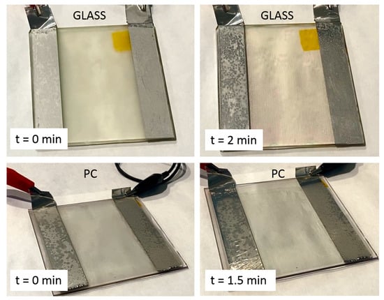
Figure 7.
Glass and PC 10 × 10 cm2 samples coated by an ITO thin film and kept in a refrigerator for 30 min at −21 °C, before and after applying a DC voltage of 8 V for 2 min.
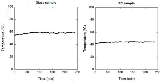
Figure 8.
Temperature measured by a thermographic camera on glass and PC samples coated by ITO thin films when applying a DC voltage of 8 V for 4 h.
4. Discussion
4.1. Effects of Oxygen Flow on Microstructural and Optoelectronic Properties of ITO Thin Films
Although all samples showed very low average surface roughness (<2.5 nm), surface morphology changed drastically with increasing the oxygen flow, as previously reported by other authors [,]. We can divide the oxygen flow range in three different regions. In each of those regions, the increase in the amount of oxygen during deposition showed different effects in the layer morphology and microstructure, and, hence, in the optoelectronic properties of the layers. Those regions are low oxygen or suboxide regions (from 0 to 1 sccm), medium or optimum oxygen regions (from 2 to 5 sccm), and high or excessive oxygen regions (above 6 sccm).
4.1.1. Low Oxygen Region or Suboxide Region (0–1 sccm)
ITO layers in this region were mainly amorphous with very smooth surface and an average surface roughness below 1 nm. A critical oxygen flow above 1 sccm was needed to crystallize the ITO layer. Many studies have stated that there is a critical oxygen flow for the crystallization of ITO films deposited below crystallization temperature (160–180 °C) [,,]. In these reports, the enhanced crystallization when introducing O2 flux was attributed, on one hand, to its effect on the promotion of the formation of stoichiometric InO3 and, on the other hand, to the production of energetic O atoms and O− ions generated at the target surface and reaching the substrate and providing enough energy to the adatoms to induce the formation of crystalline structures. The lack of oxygen input and the consequential lack of crystallization significantly affected the optoelectronic properties of the ITO layer, showing a mean optical transmission in the visible region around 65%, usually attributed to the formation of substoichiometric compounds such as InO. High resistivity values were observed ((9.2 ± 0.5) × 10−3 Ω·cm), related to the low carrier mobility (<6 cm2/V·s), which can be attributed to the higher number of carrier collisions that occur in a disordered amorphous structure.
4.1.2. Medium Oxygen—Optimum Region (2–5 sccm)
ITO crystalline layers with a (222)-oriented bcc structure were formed in this region. The increase in crystallinity caused by the higher oxygen input to the sputtering process produced a decrease in the amount of electron scatter centers (such as grain boundaries, impurities, or defects in the crystalline structure), enhancing the hall mobility (Table 1) until a maximum value of 36 cm2/V·s for 5 sccm of oxygen flow.
It is well known that charge carriers of the ITO thin films are either contributed by Sn+4 ions or oxygen vacancies. The observed opposite behavior of carrier concentration when increasing the oxygen flow during deposition was due to a decrease in the number of oxygen vacancies, which are electron donors []. Besides, oxygen combines and neutralizes Sn4+, forming Sn–O complexes and further reducing the carrier amount. The significant increase in carrier mobility while keeping the carrier concentration diminishing but in the same order of magnitude improves the conductivity of the ITO thin film, as observed by other authors in previous studies of transparent conductive electrodes []. A decrease in the number of carriers was also noticed in the transmission spectra in the NIR (near-infrared) region (Figure 4). Free carriers can be excited with photons which have wavelengths in this region; thus, if carrier concentration is high, absorption in that range will occur [,]. Therefore, ITO layers deposited with oxygen inputs which caused the highest carrier concentrations (0–3 sccm) (Table 1) showed the lowest transmission at NIR. The optical gap energy of amorphous ITO thin films increases with crystallization, increasing its optical transparency [], which is consistent with our results.
The higher VIS transmission observed in ITO layers deposited in this region was caused by the higher crystallinity of the thin films, which produced less light scattering. The change in average transmission between 2 and 5 sccm of oxygen was lower than the change between 1 and 2 sccm (Table 1). This suggests that once the ITO layer was crystallized, the increase in the VIS transmission was more gradual for higher degrees of crystallization than when the material changed from amorphous to crystalline. A shift to higher angles was observed for the (222) peak when oxygen flow varied from 4 to 5 sccm. This shift can be attributed to the stress induced in the layer by the high oxygen flow, as observed by other authors [,], who have reported an increase in the measured residual compressive stress of ITO films for the highest applied oxygen flow. They stated that this compressive stress was caused by the higher plasma bombardment energy involved in film deposition with high oxygen flow, producing more dense films.
4.1.3. High Oxygen or Oxygen Excess Region (up to 6 sccm)
As mentioned before, the contribution to carrier concentration in ITO layers arises from oxygen vacancies. Low-temperature ITO deposition with high oxygen flux significantly reduced the number of oxygen vacancies in the layer, as suggested by the abrupt reduction observed in carrier concentration. According to Lee et al. [], the excess oxygen can act like two types of scattering centers: on one hand, forming Sn+–O complexes with near Sn ions to create neutral electron scattering centers and limiting the diffusion of these ions from interstitial locations and grain boundaries into the indium cation sites []; and, on the other hand, acting like traps to capture the electron carriers. Moreover, the carrier mobility changed its behavior and decreased when oxygen flow increased from 5 to 6 sccm, because of the higher number of scattering centers. The decrease in carrier concentration had a clear influence on the optical properties of the ITO layer. A significant increase at the NIR region was observed because of the decrease in the number of NIR-absorbing free carriers.
4.2. Manufacturing of Transparent ITO Heaters
The developed 10 × 10 cm2 TH prototypes showed high optical transmission and an appropriate thermal response time (lower than 2 min). Different steady state temperatures (from 25 to 80 °C) can be reached applying low voltage (below 12 V) to adapt their performance to the requirements of the application (below 30 °C for de-icing or defogging uses, or higher for fast defrosting in automotive parts []). The voltage may need to be increased to heat larger parts (which involves larger distances between the electrodes) and maintains the good heating properties reached in our prototypes (200–600 W/m2). It is worth highlighting that these THs also exhibited uniform thermal distribution over the heating area (Figure 9), which is essential for eye comfort and for avoiding the formation of hot spots that can damage the TH []. Both THs (glass and PC) showed a great stability when exposed to saline solution.
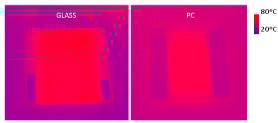
Figure 9.
Thermographic image of ITO coated glass when applying a voltage of 8 V. The square-shaped area marked in the PC image indicates a region of interest selected in this case.
5. Conclusions
Magnetron sputtering is the most useful and effective technique to deposit ITO thin films. Many methods exist to obtain high quality ITO layers, but an in-depth understanding of the deposition process is essential to grow reproducible ITO films. Small changes in certain process parameters drastically alter ITO properties. In the case of low temperature-deposited ITO, oxygen input in the process is necessary to obtain high conductivity and transparent layers. As we have confirmed, the microstructure of the material is strongly dependent on the oxygen flow, changing from amorphous to crystalline ITO layers with very small variation of oxygen amount on the gas mixture. ITO films deposited above the critical oxygen flow will be crystalline, and they will show a high transparency (>80%) in the visible region. Obtaining good electrical properties is more challenging. On one hand, it depends on the microstructure features of the layers which is directly related to the mobility of the electric carriers; On the other hand, carrier concentration is proportional to the number of oxygen vacancies and Sn+4 ions in the microstructure. Therefore, ITO films with appropriate opto-electronic properties must be grown under specific oxygen flow conditions.
Applying the found optimal oxygen flow conditions, efficient transparent ITO heaters can be manufactured by a cost-effective and robust process on glass and polymeric components, such as those used in the automotive industry (windshields or car headlights).
Author Contributions
Conceptualization, E.G.-B., L.M., and J.B.; Methodology, E.G.-B., J.T., R.O., and O.H.; Software, J.T.; Validation, J.T., E.G.-B., and L.M; Formal Analysis, J.T., E.G.-B., and R.O.; Investigation, J.T., R.O., and O.H; Resources, J.B.; Data Curation, J.T., E.G.-B., and R.O.; Writing—Original Draft Preparation, J.T., E.G.-B., and L.M.; Writing—Review & Editing, E.G.-B., R.O., and O.H.; Visualization, J.T., E.G.-B., and R.O.; Supervision, E.G.-B., L.M., and J.B.; Project Administration, E.G.-B.; Funding Acquisition, E.G.-B., L.M., and J.B. All authors have read and agreed to the published version of the manuscript.
Funding
This research received no external funding.
Data Availability Statement
Data is contained within the article.
Conflicts of Interest
The authors declare no conflict of interest.
References
- Granqvist, C.G.; Hultåker, A. Transparent and conducting ITO films: New developments and applications. Thin Solid Films 2002, 411, 1–5. [Google Scholar] [CrossRef]
- Hotovy, J.; Hüpkes, J.; Böttler, W.; Marins, E.; Spiess, L.; Kups, T.; Smirnov, V.; Hotovu, I.; Kovác, J. Sputtered ITO for applications in thin-film silicon solar cells: Relationship between structural and electrical properties. Appl. Surf. Sci. 2013, 269, 81–87. [Google Scholar] [CrossRef]
- Maniyara, R.A.; Mkhitaryan, V.K.; Chen, T.L.; Ghosh, D.S.; Pruneri, V. An antireflection transparent conductor with ultralow optical loss (<2%) and electrical resistance. Nat. Commun. 2016, 7, 13771. [Google Scholar] [CrossRef] [PubMed]
- Papanastasiou, D.T.; Schultheiss, A.; Muñoz-Rojas, D.; Cell, C.; Carella, A.; Simonato, J.P.; Bellet, D. Transparent heaters: A review. Adv. Funct. Mater. 2020, 30, 1910225. [Google Scholar] [CrossRef]
- Oxyzoglou, I.; Tejero, A. Prediction of condensation forming in automotive headlights using CFD. Tech. Rep. TOYOTA Motor Eur. 2018. [Google Scholar] [CrossRef]
- Szyszka, B.; Dewald, W.; Gurram, S.K.; Pflug, A.; Schulz, C.; Siemers, M.; Sittinger, V.; Ulrich, S. Recent developments in the field of transparent conductive oxide films for spectral selective coatings, electronics and photovoltaics. Curr. Appl. Phys. 2012, 12, S2–S11. [Google Scholar] [CrossRef]
- Elhalawaty, S.; Sivaramakrishnan, K.; Theodore, N.D.; Alford, T.L. The effect of sputtering pressure on electrical optical and structure properties of indium tin oxide on glass. Thin Solid Films 2010, 518, 3326–3331. [Google Scholar] [CrossRef]
- Park, C.H.; Lee, J.H.; Choi, B.H. Effects of the surface treatment of ITO anode layer patterned with shadow mask technology on characteristics of organic light-emitting diodes. Org. Electron. 2013, 14, 3172–3179. [Google Scholar] [CrossRef]
- Yang, C.; Lee, S.; Lin, T.; Chen, S. Electrical and optical properties of indium tin oxide films prepared on plastic substrate by radio frequency magnetron sputtering. Thin Solid Films 2008, 516, 1984–1991. [Google Scholar] [CrossRef]
- Sato, Y.; Taketomo, M.; Ito, N.; Miyamura, A.; Shigestao, Y. Comparative study on early stages of film growth for transparent conductive oxide films deposited by dc magnetron sputtering. Thin Solid Films 2008, 516, 4598–4602. [Google Scholar] [CrossRef]
- Fallah, H.R.; Ghasemi, M.; Vahid, M.J. Substrate temperature effect on transparent heat reflecting nanocrystalline IOT films prepared by electron beam evaporation. Renew. Energy 2009, 35, 1527–1530. [Google Scholar] [CrossRef]
- Viespe, C.; Nicolae, I.; Sima, C.; Grigoriu, C.; Medianu, R. ITO films deposited by advanced pulsed laser deposition. Thin Solid Films 2007, 515, 8771–8775. [Google Scholar] [CrossRef]
- Rozati, M.; Ganj, T. Transparent conductive Sn-doped indium oxide thin film deposited by spray pyrolysis techniques. Renew. Energy 2004, 29, 1671–1676. [Google Scholar] [CrossRef]
- Kurdesau, F.; Khripunov, G.; da Cunha, A.F.; Kaelin, M.; Tiwari, A.N. Comparative study of ITO layers deposited by DC and RF magnetron sputtering at room temperature. J. Non-Crystall. Solids 2006, 352, 1466–1470. [Google Scholar] [CrossRef]
- Bhagwat, S.; Howson, R.P. Use of the magnetron-sputtering technique for the control of the properties of indium tin oxide thin films. Surf. Coat. Technol. 1999, 111, 163–171. [Google Scholar] [CrossRef]
- Guillén, C.; Herrero, J. Influence of oxygen in the deposition and annealing atmosphere on the characteristic on ITO thin film prepared but sputtering at room temperature. Thin Solid Films 2005, 480–481, 129–132. [Google Scholar]
- Guillén, C.; Herrero, J. Polycrystalline growth and recrystallinization process in sputtering ITO thin films. Thin Solid Films 2006, 510, 260–264. [Google Scholar] [CrossRef]
- Morikawa, H.; Fujita, M. Crystallization and electrical property change on the annealing of amorphous indium-oxide and indium tin oxide films. Thin Solid Films 2000, 359, 61–67. [Google Scholar] [CrossRef]
- Gui, Y.; Miscuglio, M.; Ma, Z.; Tahersima, M.H.; Sun, S.; Amin, R.; Dalir, H.; Sorger, V.J. Towards integrated mecatronics: A holistic approach on precise optical and electrical properties of Indium Tin Oxide. Sci. Rep. 2019, 9, 11279. [Google Scholar] [CrossRef]
- Mudryi, A.; Ivaniukovich, A.V.; Ulyashin, A. Deposition by magnetron sputtering and characterization of indium tin oxide thin films. Thin Solid Films 2007, 515, 6489–6492. [Google Scholar] [CrossRef]
- Ghorannevis, Z.; Akbarnejad, E.; Ghoranneviss, M. Structural and morphological properties of ITO thin films grown by magnetron sputtering. Theor. Appl. Phys. 2015, 9, 285–290. [Google Scholar] [CrossRef]
- Tien, C.-L.; Lin, H.-Y.; Chang, C.-K.; Tang, C.-J. Effect of Oxygen Flow Rate on the Optical, Electrical, and Mechanical Properties of DC Sputtering ITO Thin Films. Adv. Condens. Matter Phys. 2018, 2018, 1–6. [Google Scholar] [CrossRef]
- Im, K.; Cho, K.; Kim, J.; Kim, S. Transparent heaters based on solution-processed indium tin oxide nanoparticles. Thin Solid Films 2010, 518, 3960–3963. [Google Scholar] [CrossRef]
- Kim, C.; Park, J.W.; Kim, J.; Hong, S.J.; Lee, M.J. A highly efficient indium tin oxide nanoparticles (ITO-NPs) transparent heater based on solution-process optimized with oxygen vacancy control. J. Alloys Compd. 2017, 726, 712–719. [Google Scholar] [CrossRef]
- Moon, C.S.; Han, J.G. Low temperature synthesis of ITO thin film on polymer in Ar2/H2 plasm by pulsed DC magnetron sputtering. Thin Solid Films 2008, 516, 6560–6564. [Google Scholar] [CrossRef]
- Bouroushian, M. Characterization of Thin Films by Low Incidence X-Ray Diffraction. Cryst. Struct. Theory Appl. 2012, 1, 35–39. [Google Scholar] [CrossRef]
- Coating of Glass Optical Elements (Anti-Reflection). Military Specification, MIL-C-675C. 1980. Available online: https://www.irdglass.com/wp-content/uploads/2016/07/MIL-C-675C-AR-coatings.pdf (accessed on 14 January 2021).
- Dutta, J.; Ray, S. Variation in structural and electrical properties of magnetron-sputtered Indium Tin Oxide films with deposition parameters. Thin Solid Films 1988, 162, 119–127. [Google Scholar] [CrossRef]
- Haacke, G.J. New figure of merit for transparent conductors. J. Appl. Phys. 1976, 47, 4086. [Google Scholar] [CrossRef]
- Xian, S.; Nie, L.; Qin, J.; Kang, T.; Li, C.; Xie, J.; Deng, L.; Lei, B. Effect of oxygen stoichiometry on the structure, optical and epsilon-near-zero properties of indium tin oxide films. Opt. Express 2019, 27, 28618–28628. [Google Scholar] [CrossRef]
- Munir, M.M.; Iskandar, F.; Yun, K.M.; Okuyama, K.; Abdullah, M. Optical and electrical properties of indium tin oxide nanofibers prepared by electrospinning. Nanotechnology 2008, 19, 145603. [Google Scholar] [CrossRef]
- Buchanan, M.; Webb, J.B.; Williams, D.F. Preparation of conducting and transparent thin films of tin-doped indium oxide by magnetron sputtering. Appl. Phys. Lett. 1980, 37, 213–215. [Google Scholar] [CrossRef]
- Hoshi, Y.; Kato, H.; Funatsu, K. Structure and electrical properties of ITO thin films deposited at high rate by facing target sputtering. Thin Solid Films 2003, 445, 245–250. [Google Scholar] [CrossRef]
- Vink, T.J.; Walrave, W.; Daams, J.L.C.; Baarslag, P.C.; van den Meerakker, J.E.A.M. On the homogeneity of sputter-deposited ITO films Part I. Stress and microstructure. Thin Solid Films 1995, 266, 145–151. [Google Scholar] [CrossRef]
- Fan, J.C.C.; Goodenough, J.B. X-ray photoemission spectroscopy studies of Sn-doped indium-oxide films. J. Appl. Phys. 1977, 48, 3524–3531. [Google Scholar] [CrossRef]
- Masis, M.M.; De Wolf, S.; Woods-Robinson, R.; Ager, J.W.; Ballif, C. Transparent Electrodes for Efficient Optoelectronic. Adv. Electron. Mater. 2017, 3, 1600529. [Google Scholar] [CrossRef]
- Wong, F.L.; Fung, M.K.; Tong, S.W.; Lee, C.S.; Lee, S.T. Flexible organic light-emitting device based on magnetron sputtered indium-tin-oxide on plastic substrate. Thin Solid Films 2004, 466, 225–230. [Google Scholar] [CrossRef]
- Kim, J.; Shrestha, S.; Souri, M.; Connell, J.G.; Park, S.; Seo, A. High-temperature optical properties of indium tin oxide thin-films. Nat. Res. Sci. Rep. 2020, 10, 12486. [Google Scholar] [CrossRef]
- Lee, H.C.; Ok Park, O. Behaviours of carrier concentrations and mobilities in indium-tin oxide thin films by DC magnetron sputtering at various oxygen flow rates. Vacuum 2004, 77, 69–77. [Google Scholar] [CrossRef]
- Khaligh, H.H.; Xu, L.; Khosropour, A.; Madeira, A.; Romano, M.; Pradére, C.; Tréguer-Delapierre, M.; Servant, L.; Pope, M.A.; Goldthorpe, I.A. The Joule heating problem in silver nanowire transparent electrodes. Nanotechnology 2017, 28, 425703. [Google Scholar] [CrossRef]
Publisher’s Note: MDPI stays neutral with regard to jurisdictional claims in published maps and institutional affiliations. |
© 2021 by the authors. Licensee MDPI, Basel, Switzerland. This article is an open access article distributed under the terms and conditions of the Creative Commons Attribution (CC BY) license (http://creativecommons.org/licenses/by/4.0/).