Abstract
Titanium oxide films were deposited at room temperature and with no applied bias using a filtered cathodic vacuum arc (FCVA) system in a reactive oxygen environment. The dependence of film growth on two process parameters, the working pressure (Pw) and the O2 partial pressure (pO2), is described in detail. The composition, morphological features, crystalline structure, and optical properties of the deposited films were systematically studied by Rutherford Back Scattering (RBS), Scanning Electron Microscopy (SEM), X-Ray diffraction (XRD), Raman Spectroscopy, UV-vis spectroscopy, and spectroscopic ellipsometry. This systematic investigation allowed the identification of three different groups or growth regimes according to the stoichiometry and the phase structure of the titanium oxide films. RBS analysis revealed that a wide range of TiOx stoichiometries (0.6 < × < 2.2) were obtained, including oxygen-deficient, stoichiometric TiO2 and oxygen-rich films. TiO, Ti2O3, rutile-type TiO2, and amorphous TiO2 phase structures could be achieved, as confirmed both by Raman and XRD. Therefore, the results showed a highly versatile approach, in which different titanium oxide stoichiometries and crystalline phases especially suited for diverse optical applications can be obtained by changing only two process parameters, in a process at room temperature and without applied bias. Of particular interest are crystalline rutile films with high density to be used in ultra-high reflectance metal-dielectric multilayered mirrors, and reduced-TiO2 rutile samples with absorption in the visible range as a very promising photocatalyst material.
1. Introduction
Great attention has been focused on the different polymorphs and stoichiometries of titanium oxide thin films due to their application in a wide range of fields [1]. In the case of TiO2 films, different crystalline phases are described, namely anatase, rutile, and brookite, which determine its properties and applications. The first two phases are the most used for technological applications. TiO2 films with anatase phase are used as self-cleaning windows, antifogging glass, self-sterilizing, and anti-bacterial tiles, as well as for water purification devices [2]. Anatase TiO2 is also known for its use as a photoanode in Dye Sensitized Solar Cells [3]. Among the TiO2 phases, the rutile phase is chemically and thermodynamically more stable and has the highest refractive index and hardness [4]. Some technological applications of rutile films include its use as optical coatings, as a dielectric layer in microelectronic applications, and as a protective layer on biomedical implants [5]. Rutile-type TiO2 films can be especially suited as the high refractive index material of choice in combination with a low refractive index material as SiO2 to achieve highly reflecting multilayer stacks in dielectric mirrors [6]. Regarding amorphous TiO2, it has been synthesized as a tinted or enhanced photocatalyst, used to purify dye-polluted water, and applied to resistive random access memory applications [7].
In addition to the possibility to fabricate different crystalline phases, the desired properties of the TiO2 films can be tuned by slight changes in their stoichiometry. TiO2 is a wide bandgap semiconductor (3.0 and 3.2 eV for rutile and anatase, respectively), which is photoactive when irradiated with UV light. To widen the use of TiO2 as a photocatalyst, its activity needs to be extended beyond the ultraviolet regime into the visible region [8]. In oxygen-deficient TiOx films (x < 2), oxygen vacancy energy states are formed below the conduction band minimum [8]. This results in a reduction in the energy required for photoexcitation of electrons, making it possible for the films to absorb visible light. Oxygen-deficient TiO2 films also have potential application as electrode material for alkaline-electrolyte batteries since they can be electrically conductive and yet maintain their corrosion-resistant properties [9]. However, there is no industrially scalable process available for high throughput synthesis of oxygen-deficient TiO2.
The final properties of titanium oxide films strongly depend on the deposition technique employed for their fabrication (i.e., sol-gel, Chemical Vapour Deposition (CVD), Physical Vapour Deposition (PVD)). In particular, TiO2 films deposited at low temperatures by most deposition methods exhibit an amorphous phase. Film crystallization is usually performed either by substrate heating during deposition or by a post-deposition annealing process. In addition, in PVD processes, very often the application of a bias to the substrate is required to obtain TiO2 crystalline films. However, a myriad of recent applications require the TiO2 films to be coated on heat-sensitive and/or non-conductive substrates (e.g., flexible electronics, antireflective coatings on plastic lenses, etc.). Therefore, it is important to optimize growth conditions in order to obtain crystalline films and/or the desired stoichiometry at low temperature using any type of substrate. To achieve that, it would be interesting to rely on other parameters of the deposition process different from the applied bias or the temperature. In this regard, there are some previous studies on the effect of the working pressure and the O2 partial pressure on titanium oxide film formation [4,10].
Among the different PVD techniques, filtered cathodic vacuum arc (FCVA) has the highest plasma ionization ratio. This results in denser thin films and better adhesion than those obtained by technologies like magnetron sputtering or thermal evaporation [11]. Hence, this technique is especially suited for optical applications. The substrate temperature and the ion energy mainly determine phase formation during deposition by FCVA. In the case of TiO2, amorphous films are obtained at low temperature and low ion energy. Therefore, synthesizing crystalline TiO2 by FCVA usually requires either heating or biasing the substrate during deposition [5,12]. The phase diagram proposed by Löbl et al. [13] shows that with particle energies between 4–30 eV, mixed phases of rutile and anatase can be obtained at room temperature, meanwhile only at particle energies over 30 eV pure rutile phases can be obtained. These high ion energies are in the range of a FCVA deposition process.
In this work, a systematic study of the effect on titanium oxide films of the working pressure and oxygen partial pressure in a FCVA deposition process is carried out. We demonstrate that a fine tune of these parameters leads to the formation of a wide variety of stoichiometries and crystalline phases, from amorphous to rutile, at room temperature without the application of any bias during the deposition.
2. Materials and Methods
Titanium oxide films were grown on Si (100) and on glass substrates by means of a DC Filtered Cathodic Vacuum Arc (FCVA) system PFCVA-450 from Plasma Technology Limited, Hong Kong. The system is provided by a 90° curved electromagnetic filter which guides the ions in the plasma to the deposition chamber. The substrates were placed 240 mm away from the filter duct exit. For each deposition process, base pressure in the chamber was ~2 × 10⁻³ Pa. Prior to deposition, samples were sputter cleaned by Ar+ bombardment for 15 min. In a FCVA system like the one used in this work, when no bias is applied during the process, the temperature at the surface of the sample reaches a maximum of ~100 °C after 40 min of deposition process. A Ti cathode with 65 mm diameter was used for the deposition of the films in an oxygen/argon atmosphere. The total working gas flow was fixed at 60 sccm, and different percentages of reactive gas during depositions were obtained by changing the Ar/O2 ratio. The cathode current used was 50 A. All the depositions processes were carried out at room temperature. Deposition time was 15 min and the substrate holder was rotating during the whole process at 5 rpm. Depth-resolved composition of the samples was determined by Rutherford backscattering spectroscopy (RBS) using 4+He incident ions with an energy beam of 1.7 MeV. The data were acquired with a silicon barrier detector located at a backscattering angle of 170°, with an energy detector resolution of 13 keV. The experimental spectra were fitted using the SIMNRA software [14]. The thickness of the films was measured using a mechanical stylus profilometer (Veeco Dektak 150). Morphology was analyzed by scanning electron microscopy (SEM) with a Hitachi S4800 SEM-FEG microscope of high resolution (1–3 nm), equipped with a Bruker X flash 4010 EDX detector with a resolution of 133 eV, field emission gun, and STEM detector system. The phase structure of the thin films was determined by X-ray diffraction employing grazing incidence geometry (GIXRD) using a Rigaku Ultima IV diffractometer with Cu-Kα radiation (λ = 1.5406 Å). The incident angle was 0.4°, and the XRD patterns were measured in the diffraction angle range of 20–100° in steps of 0.02°. Raman spectra were measured in 180° backscattering geometry using a micro Raman LabramHR system (Horiba GmbH) equipped with a LN2 cooled CCD detector. For excitation, the frequency-doubled 532 nm emission of a Nd:YAG laser was focused to a 1 µm spot with 1 mW power on the sample surface. Spectroscopic Ellipsometry (SE) was used to determine the refractive index n of the samples. Measurements were performed with a rotating compensator ellipsometer M-2000FI (J.A. Woollam, Inc.) in the wavelength range of 211–1688 nm with a fixed angle of polarized light incidence and reflection of 75°.
3. Results
3.1. Thin Film Growth and Film Composition
The deposition of the films was performed at three different working pressures (Pw), 0.1, 0.25, and 0.5 Pa. For each Pw, the oxygen/argon ratio was varied by changing the O2 gas flow from ~20 to ~80%. Consequently, the oxygen partial pressure (pO2) during deposition ranged from 0.02 to 0.41 Pa. The O/Ti ratio for the different films obtained by RBS are shown in Figure 1. RBS profiles (not shown) indicated that the composition is uniform through the thickness of the films. It was found that the samples could be divided into three main groups according to their stoichiometry. In Figure 1, it is shown that the group 1 (G1) samples have an O/Ti ratio lower than 2 (0.6 ≤ O/Ti ≤ 1.6), samples in group 2 (G2) exhibit an O/Ti close to 2 (1.9 ≤ O/Ti ≤ 2.0), and finally, samples belonging to group 3 (G3) have an O/Ti ratio higher than 2 (O/Ti ≥ 2.1). This classification of the deposited films in three different groups is further supported by the differences in crystallinity of the samples, as will be shown by XRD and Raman results in Section 3.2. G1 samples are obtained at the lowest working pressure (0.1 Pa) or at the intermediate pressure (0.25 Pa) and low oxygen partial pressure (<0.1 Pa). Stoichiometric TiO2 samples in G2 can be obtained at 0.25 Pa working pressure provided that the pO2 is over a threshold value of~> 0.1 Pa. Finally, over stoichiometric (G3) films are obtained for the working pressure of 0.5 Pa in the entire oxygen partial pressure range analyzed.
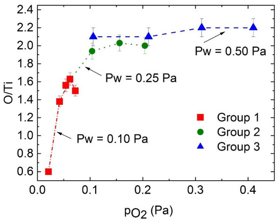
Figure 1.
O/Ti ratio obtained from RBS for the different samples as a function of pO2. The different groups are indicated by color and legend code: group 1 (square, red), group 2 (circle, green) and group 3 (triangle, blue). Samples deposited at the same Pw are connected through lines, and the value of the working pressure is indicated in the graph.
In Figure 2, a summary of the different deposited samples is depicted, indicating the three identified groups. All the samples in G1 are opaque. With respect to G2, visual inspection revealed that a slight variation in the stoichiometry of the samples (from O/Ti = 1.9 to O/Ti = 2) led to strong variation in transmittance. This can be observed by comparing G2 samples prepared at % O2 gas flow of 40% and 60%. For the former, a reduced TiO2 material is obtained (O/Ti = 1.9). TiO2 bulk reduction results in color centers, which produce a pronounced color change of TiO2 single crystals from initially transparent to visible light to eventually exhibiting a dark blue colour [2]. A similar result is observed in the current work for the reduced TiO2 sample, which exhibits a blueish color. The stoichiometric TiO2 samples prepared at 60 and 80% O2 gas flow are transparent, as expected for a wide band gap semiconductor. Finally, all G3 samples are transparent, regardless of the oxygen partial pressure used during the deposition process.
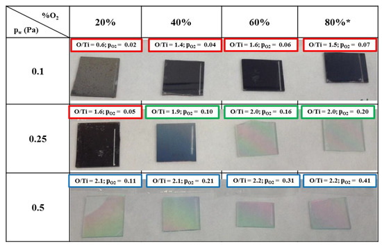
Figure 2.
Summary table of deposited samples with varying % of Ar/O2 gas flow, and Pw including: picture of each sample deposited on glass, pO2 during deposition and elemental at.% (O/Ti ratio) obtained by RBS. The code color indicates the samples belonging to group 1 (red), 2 (green), and 3 (blue). * For the lower working pressure (0.1 Pa), it was not possible to perform the deposition process with more than 70% of oxygen gas flow.
In Figure 3, the thicknesses of the different samples obtained by profilometry are plotted as a function of the oxygen partial pressure, indicating also the samples that were deposited at the same working pressure. A gradient color can be observed in transparent samples due to interferences (Figure 2), which must be caused by non-homogeneity of the thickness along the substrate. For this reason, at least three measures of the thickness in different substrate positions were performed and the average and error values were obtained.
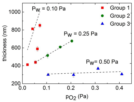
Figure 3.
Coating thickness on silicon as a function of pO2 for samples belonging to group 1 (square, red), 2 (circle, green), and 3 (triangle, blue). A linear fit has been obtained for the samples deposited with the same working pressure. The total deposition time was 15 min in all cases.
It is observed that the sample thickness is affected by both, the pO2 and the Pw. Higher thicknesses are obtained for lower working pressures and/or lower oxygen partial pressures. However, the working pressure is the factor that affects final thickness the most. For similar pO2 around 0.2 Pa, a sample deposited at Pw 0.25 Pa exhibits ~700 nm thickness, and one deposited at Pw 0.50 Pa is only 300 nm thick. At similar oxygen partial pressure, thickness decreases with working pressure, as the main free path of the species diminishes. Deposition rates were ~56 nm/min for G1, 45 nm/min for G2, and 24 nm/min for G3.
Provided the film thickness is known from profilometry, the density of TiO2 films can be obtained from RBS data [15]. Samples in G2 exhibit a density ~4.5 g cm−3, meanwhile the density of samples in G3 is ~3.6 g cm−3. As will be shown later, these results are in line with the crystallinity of the samples. Bulk theoretical values are 4.23 g cm−3 for rutile and 3.6 g cm−3 for amorphous TiO2 [16]. Bendavid et al. [17] reported a density of 3.62 g cm−3 for TiO2 amorphous films deposited by FCVA.
3.2. Structure and Morphology
Cross-sectional SEM analysis of the morphology revealed remarkable differences among the three groups. A columnar structure is observed for G1. High energy particle bombardment at low pressure can be the cause for the elongated faceted texture of the film (Figure 4a,b). For G2, two growth regimes are observed in the SEM images. During the first stages of the deposition process, the samples grow without any type of texturized structure (up to approximately 300 nm). Subsequently, the films develop a clear columnar structure (Figure 4c,d). This is also in line with the crystallinity observed in G2 samples, as confirmed by XRD experiments. Less energetic particle bombardment at higher pressure resulted in featureless and non-textured films, which is an indication of amorphous nature in G3 samples (Figure 4e,f).
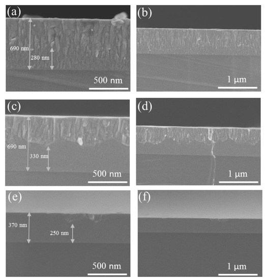
Figure 4.
Representative SEM cross-section images for samples for G1 (a,b), sample deposited at Pw 0.1 Pa, pO2 = 0.06 Pa; G2 (c,d), sample deposited at Pw 0.25 Pa, pO2 = 0.20 Pa; and G3 (e,f), at Pw 0.5 Pa, pO2 = 0.31 Pa.
The Glancing Incidence XRD (GIXRD) patterns of selected films for the different groups are represented in Figure 5 and Figure 6. For the crystalline samples, interplanar spacing (d) and lattice constants (a and c) were calculated as an average of the main observed peaks. The crystallite sizes obtained from Scherrer’s formula [18] are also calculated for the TiO2 stoichiometric samples. The results are summarized in Table 1.
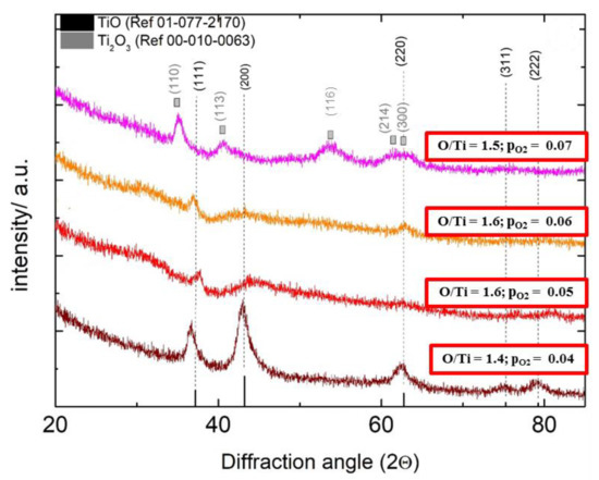
Figure 5.
GIXRD patterns for samples of G1 deposited on silicon substrates. TiO and Ti2O3 reference peaks are included in the graph.
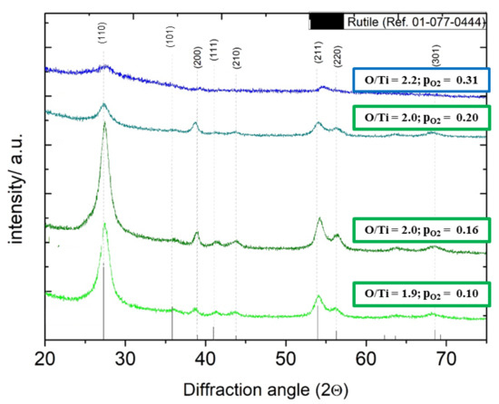
Figure 6.
Glancing incidence XRD patterns for samples of G2, and a representative sample of G3. Rutile-type TiO2 reference peaks are included in the graph.

Table 1.
Peak position, crystal planes, interplanar spacing, and lattice constants for TiO and Ti2O3 reference cards and samples in group 1.
In Figure 5, the diffractograms for the samples belonging to G1 are plotted. No peaks related to any TiO2 crystalline phases are observed. For samples with pO2 of 0.04, 0.05, and 0.06 Pa, despite the different stoichiometries, the peaks can be attributed to TiO (ICC card 01-077-2170) with a cubic structure, (rock-salt space group 225, Fm-3m) in all the samples. Reference crystal peaks at 2θ = 36.60°, 42.87°, 62.38°, and 75.01° are associated with the crystal planes (111), (200), (220), and (311), respectively. For the sample with the strongest diffraction peaks in G1 (pO2 = 0.04), the diffraction peaks appear at slightly smaller diffraction angles (between 0.2 and 0.5°), corresponding to a larger lattice constant of the rocksalt-type sample than in the reference data set of TiO. The sample deposited at pO2 = 0.07 (O/Ti ratio of 1.5) shows diffraction peaks at 2θ = 35.00°, 40.66° and 54.21°. These peaks can be attributed to Ti2O3 (ICC card 00-010-0063), space group 167, R-3c, corresponding to the crystal planes (110), (113), and (116), respectively. Around 2θ = 62° a broad peak is observed which can be related to the contribution of crystal planes (214) and (300), related to peaks at 61.34° and 62.58° in the reference card (see Table 1). In general, the peaks are very broad, except for the one at 2θ = 35.00°. Parker et al [19] reported on the formation of the Ti2O3 layer by bombardment with Kr ions on TiO2. A high dose ion impact led to preferential oxygen sputtering and/or internal precipitation of oxygen. Ion energy is higher in cathodic arc vacuum deposition, so, in the current work, the Ti2O3 phase could be formed at low working pressures (where high ion energy of the ions is expected) and with a high oxygen partial pressure.
A completely different scenario is observed for the three samples belonging to group 2 (Figure 6 and Table 2). The diffractograms of samples belonging to this group showed a pattern corresponding to rutile TiO2 with tetragonal structure (space group 136, P42-mnm). The main rutile peak (110) is observed at 2θ = 27.39°, 27.38° and 27.3° for samples with pO2 of 0.10, 0.16, and 0.20 Pa, respectively. Hence these peaks are slightly shifted to higher angles with respect to the reference pattern (2θ = 27.29°) for this crystal plane (110). The other main peaks are observed at 2θ~54° and 56°, related to crystal planes (211) and (220). These three main peaks have been selected to calculate the lattice parameter (a and c) and the crystallite size. Other minor peaks confirming the rutile phase observed at 2θ~38.97, 40.97, 43.80, and 68.56° are associated to the crystal planes (200), (111), (210), and (301), respectively, according to the reference card.
Table 2.
Peak position, crystal planes, interplanar spacing, and lattice constants for TiO2 rutile reference cards and for samples in group 2.
Finally, all group 3 samples showed only few broad and weak diffraction peaks, pointing to a predominantly X-ray amorphous phase structure with few nanocrystalline regions. See for example the diffractogram in Figure 6 corresponding to samples deposited at 0.31 Pa of pO2. This phase structure can be related to the higher working pressure, and therefore to the lower energy of species impinging on the substrate. Only a small and very wide peak can be inferred at angles corresponding to the crystal plane (110) of the rutile phase. The rutile (110) surface is the most stable crystal face [2]. In the case of vapor deposition, the different crystallographic planes grow at different rates depending on their surface formation energies. The slight crystallization observed for films in G3 in the rutile phase for the plane (110) can be attributed to the lower surface formation energy of this plane [4]. In relation to the SEM results, this can be an indication of a change in the growth regime that could lead to crystalline structures.
Raman spectroscopy confirmed and complemented the data obtained by X-ray diffraction. For G1 samples grown at the oxygen partial pressures of 0.02 Pa ≤ pO2 < 0.06 Pa, the Raman spectra exhibit two broad band-like features centered at around 250 cm−1 and at around 550 cm−1 (Figure 7). The corresponding line widths of 200 to 300 cm−1 are typical for phonon density of states-like Raman spectra of amorphous materials. It is tempting to attribute the low-energy band (50 to 350 cm−1) to titanium-based phonon states, and the high-energy band (400 to 700 cm−1) to oxygen phonon-based states. Thus, the Raman spectra indicate a significant amount of amorphous structures, in addition to the fraction of rock salt-type TiO detected by XRD. Since crystalline TiO is Raman-silent, the combination of XRD and Raman data point to the coexistence of nanocrystalline and amorphous TiO in these four samples of G1. The Raman spectrum of the sample grown at an oxygen pressure of 0.07 Pa shows, in addition to broad lines at the same positions as those of the other four G1 samples, several narrower features (Figure 7). The most prominent ones among them, located at 263 cm−1 and 334 cm−1, can be assigned to the most prominent lines reported for Ti2O3 at 269 cm−1 and 347 cm−1 (vertical bars in Figure 7) [20]. The observation of these lines supports the finding of Ti2O3 by XRD. Moreover, the Raman spectra reveal a significant amorphous phase fraction within the film grown at an oxygen pressure of 0.07 Pa at a working pressure of 0.10 Pa.
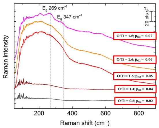
Figure 7.
Raman spectra of samples in G1. Ti2O3 lines from Ref. [20] are indicated in the graph. The spectra were offset vertically for better visibility.
The Raman spectra of the films grown at a working pressure of 0.25 Pa with an oxygen partial pressure of 0.10 to 0.20 Pa (G2 samples) are dominated by strong lines at 450 ± 2 cm−1 and 608 ± 3 cm−1 (Figure 8). These lines point to the presence of nano-crystalline rutile-type TiO2, whose strongest Raman lines are the Eg line at 447 cm−1 and the A1g line at 612 cm−1 [21]. The line positions found for the films grown in this work are close to the literature values, shifted by +3 (Eg) and by −4 cm−1 (A1g), respectively. The observed downshift of the A1g line might be caused by the small size of the rutile-type TiO2 crystals grown here. According to Swamy et al. a shift of −4 cm−1 would indicate a crystallite size of 10 nm [22]. This value is in very good agreement with that of 6 nm obtained by XRD for these samples (Table 2).
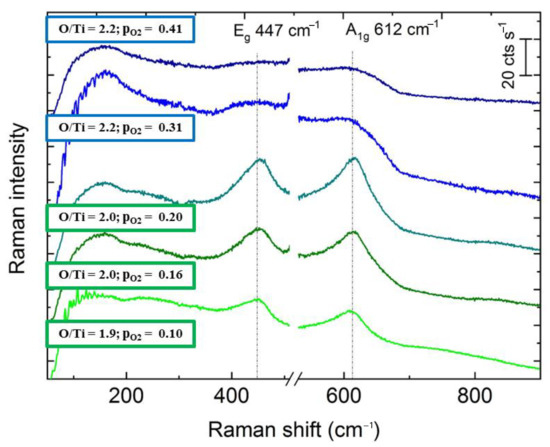
Figure 8.
Raman spectra of samples in G2 and G3. Reference lines for the Eg and A1g positions of rutile-type TiO2 are included in the graph. Spectra were offset vertically for better visibility. The contribution of Si at 20 cm−1 was removed from the graph.
The Raman spectra of films belonging to group 3 exhibit two broad Raman lines at around 460 cm−1 and 608 cm−1 that indicate the presence of nanocrystalline Rutile-type TiO2 in coexistence with the amorphous phase (Figure 8). According to Parker et al., the Eg line frequency scales linearly with the oxygen content in rutile-type TiO2 [23]. Hence, the observed upshift of the Eg-derived line to 460 cm−1 in the G3 samples, compared to the Eg at 447 cm−1 in single crystals, can be qualitatively explained by the oxygen excess (O/Ti = 2.2) detected by RBS. The origin of the A1g line downshift by −4 cm−1 compared to the reference value is presumably the same as for the G2 samples.
3.3. Optical Properties
Spectral transmittance and ellipsometry measurements were performed to correlate the changes observed in the stoichiometry and crystallinity of the films with their optical properties. Figure 9 shows the transmittance spectra of the films deposited on glass substrates for samples of the three different groups. Only stoichiometric samples or samples with O/Ti ≥ 2 exhibit a high transmittance in the visible and near IR region, in agreement with the images of the samples depicted in Figure 2. The transmission spectrum of G1 (O/Ti = 1.6) consists of a straight line in the whole UV-Vis-NIR. It is therefore a broad band absorber, presumably based on different color centers from differently charged ions (Ti2+, Ti3+ (Ti+)) and maybe oxygen vacancies.
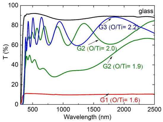
Figure 9.
Transmittance of selected representative samples deposited on glass. The reference was air and the spectrum of glass substrate is also included in the graph. The code color indicates the samples belonging to group 1 (red), 2 (green), and 3 (blue), and the O/Ti ratio of the different samples is indicated next to each line.
As mentioned above, the transmittance of TiO2 thin films is very sensitive to slight variation in the stoichiometry. The G2 sample deposited at pO2 = 0.1 Pa can be considered a reduced rutile sample. Breckenridge and Hosler [24] reported light absorption in the visible region in the case of slightly reduced oxygen-deficient TiO2. Reduced rutile could imply some fraction of Ti3+, or two O2− vacancies for one Ti4+. Several authors have reported the fabrication of reduced TiO2 films [8,25,26].
In Figure 10, the spectral refractive indexes (a) and extinction coefficients (b) of representative samples for each group obtained from ellipsometry measurements are shown. Several groups have studied the optical constants of titanium oxide thin films under various deposition conditions. Refractive index and extinction coefficient both tended to decrease as the working pressure increases [9]. In contrast, in this work, there is no direct relation with the total working pressure, as the refractive index is highly dependent on the crystalline phase of the TiO2. In general, amorphous films show a lower refractive index than that of crystalline film. Rutile structure exhibits the highest refractive index due to its superior density among all the TiO2 phases. In this work, refractive indexes at a wavelength of 550 nm were 1.56, 2.63, and 2.57, measured for representative samples of groups 1, 2, and 3, respectively. The higher value of the refractive index obtained for group 2 is in line with the crystalline rutile structures observed in XRD and Raman. A refractive index of 2.57 at 550 nm (similar to the obtained for G3 samples) has been reported in the literature for amorphous TiO2 films deposited at RT with no bias by FCVA [27]. This n is higher than the one obtained for amorphous films with other deposition techniques [9], due to the enhanced reactivity and high energy of the Ti ion beam impinging on the growing TiO2 films by FCVA.
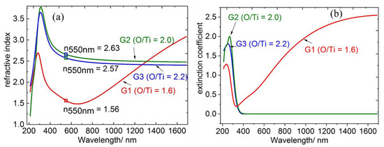
Figure 10.
Refractive index (a) and extinction coefficient (b) in the 200–1700 nm wavelength range for one representative sample of group 1 (red), 2 (green), and 3 (blue). The refractive index at 550 nm is marked as an open square and the actual value is included in the graph.
4. Discussion
Titanium oxide films were grown by FCVA and the influence of the total working pressure and the oxygen partial pressure during the deposition process was systematically studied. A strong correlation between those parameters and the properties of the films was found, and three different growth regimes or groups were identified.
Samples belonging to group 1 were obtained (i) with the lowest working pressure used in this work (Pw = 0.1 Pa) and, (ii) with the intermediate pressure (Pw = 0.25 Pa) if the oxygen partial pressure was below 0.1 Pa. These samples exhibited a columnar structure in the SEM cross-section images and were opaque. Besides, all the samples shared an O/Ti ratio < 2, and the presence of crystalline phases different fromTiO2. For samples with a pO2 of 0.04, 0.05, and 0.06 Pa, the combination of XRD and Raman pointed out the coexistence of nanocrystalline and amorphous TiO. For the samples deposited at pO2 = 0.7 Pa, both XRD and Raman revealed features, which were attributed to Ti2O3. The Raman spectra also revealed a significant amount of amorphous Ti2O3 phase in this film.
In the range corresponding to intermediate working pressures (0.25 Pa) and oxygen partial pressure above 0.10 Pa, we found the samples forming group 2. In addition to a stoichiometry close to TiO2, they shared their crystalline structure. Both XRD and Raman indicated that the samples in this group exhibited a rutile TiO2 structure. This crystalline structure provided the samples of this group with very interesting properties for optical applications. The rutile crystalline structure and the high film density (~4.5 g cm−3) led to a higher refractive index (n550nm = 2.62) in comparison to amorphous TiO2 or rutile TiO2 fabricated with less energetic deposition techniques and obtained by post-annealing processes. Samples of this group are very promising, for example, as high refractive index dielectric material in ultra-high reflectance metal-dielectric multilayered mirrors [6]. The sample deposited with the lowest oxygen partial pressure (pO2 = 0.10 Pa) is worthy of note. It exhibited similar characteristics to the other samples belonging to this group, with a stoichiometry close to TiO2 and a rutile phase structure. However, contrary to them, it is not transparent but exhibited a blueish colour and was absorbed in the visible region. This reduced TiO2 sample is very interesting as it preserves the properties of crystalline rutile TiO2, while, and at the same time is photoactive in the visible region, being a very promising photocatalyst material, among other applications.
Finally, samples belonging to group 3 were obtained with the highest working pressure (Pw = 0.5 Pa), regardless of the oxygen partial pressure. All the samples are transparent and exhibit oxygen excess with O/Ti ratios above 2.1. The combination of SEM images, the lower values for density and refractive index compared to group 2, together with XRD and Raman results, pointed out the amorphous phase structure of these samples. However, a tendency of growth regimes from amorphous to crystalline TiO2 could be inferred from a small rutile peak in XRD and broad Raman lines for Rutile- type TiO2.
A summary of properties reported for TiO2 films deposited by FCVA in previous references is included in Table 3. A final line has been added to the table with the results obtained in the current work.
Table 3.
Summary of previous references of TiO2 films deposited using FCVA, including information about the applied bias, temperature and working pressure during deposition, the observed crystalline phase, and the refractive index. The results observed in the current work are included in the last row.
It is commonly observed in PVD that the phase formation is mainly determined by the temperature and ion energy [41]. At room temperature, without external heating and substrate bias, titanium oxide thin films deposited by FCVA are usually amorphous in structure [9]. Zhang et al. [29] observed that when the substrate bias was −100 V, films exhibited rutile-type structure with XRD (110), (101), and (111) diffraction peaks, the (111) peak being dominant. These authors further demonstrated that without bias, the film structure remained amorphous. This is a result generally observed, as shown in Table 3. Some exceptions are found, for example in the works by Bendavid et al. [17,30]. These authors reported an anatase structure without substrate bias at room temperature at an oxygen pressure of 0.35 Pa. When the substrate bias was applied from zero to −400 V, the film structure varied from anatase (0 V) to amorphous phase at −50 V, evolving into a rutile structure with (101) orientation dominating in the films when the applied voltage is <−100 V. These authors ascribed the formation of the rutile phase to two concurrent factors: (i) the high concentration of ionic species (e.g., Ti+), a typical feature of plasma produced by FCVA, and (ii) the high energy of particles impinging on the substrate, due to the applied bias [17,30].
However, in the present work, XRD and Raman indicated that the rutile phase was obtained at room temperature without the need for any applied bias. Besides, no anatase phase formation was observed within the range of studied process parameters, although the rutile phase usually requires higher activation energy for its formation [42]. This is, to the best knowledge of the authors, the first time that the fabrication of rutile-type TiO2 at low temperature with no applied bias is reported for a FCVA process. This paves the way for the deposition of this TiO2 crystalline phase with outstanding optical properties in transparent substrates such as glass, which is non-conductive and also on heat-sensitive substrates.
In summary, this work describes a very versatile method for the deposition of titanium oxide films with different stoichiometries and crystalline phases, demonstrating the great potential of FCVA for the deposition of these films for optical applications.
Author Contributions
Conceptualization, E.G., M.K. and R.E.-G.; Data curation, E.G.; Formal analysis, E.G., M.K. and R.E.-G.; Investigation, E.G., I.H. and G.R.-L.; Methodology, R.E.-G.; Project administration, R.E.-G.; Supervision, R.E.-G.; Visualization, E.G.; Writing—original draft E.G., M.K. and R.E.-G.; Writing—review & editing, E.G., M.K., I.H., G.R.-L. and R.E.-G. All authors have read and agreed to the published version of the manuscript.
Funding
This project was partially supported by H2020 RISE project “Framework of Innovation for Engineering of New Durable Solar Surfaces (FRIENDS2, GA-645725)”.
Institutional Review Board Statement
Not applicable.
Informed Consent Statement
Not applicable.
Data Availability Statement
Not applicable.
Acknowledgments
Support by the Ion Beam Centre (IBC, Helmholtz-Zentrum Dresden-Rossendorf) is gratefully acknowledged. The authors would like to thank Ma C. Jiménez de Haro (Instituto Ciencia y Tecnología de Materiales de Sevilla) for the SEM service. Any opinions, findings, and conclusions or recommendations expressed in this material are those of the authors and do not necessarily reflect those of the host institutions or funders.
Conflicts of Interest
The authors declare no conflict of interest.
References
- Chen, X.; Mao, S.S. Titanium dioxide nanomaterials: Synthesis, properties, modifications, and applications. Chem. Rev. 2007, 107, 2891–2959. [Google Scholar] [CrossRef]
- Diebold, U. The Surface Science of Titanium Dioxide. Surf. Sci. Rep. 2003, 48, 53–229. [Google Scholar] [CrossRef]
- Aramwit, C.; Intarasiri, S.; Bootkul, D.; Tippawan, U.; Supsermpol, B.; Seanphinit, N.; Ruangkul, W.; Yu, L. Effects of Filtered Cathodic Vacuum Arc Deposition (FCVAD) Conditions on Photovoltaic TiO2 Films. Appl. Surf. Sci. 2014, 310, 266–271. [Google Scholar] [CrossRef]
- Pradhan, S.S.; Pradhan, S.; Bhavanasi, V.; Sahoo, S.; Sarangi, S.; Anwar, S.; Barhai, P. Low Temperature Stabilized Rutile Phase TiO2 Films Grown by Sputtering. Thin Solid Films 2012, 520, 1809–1813. [Google Scholar] [CrossRef]
- Arias, L.M.F.; Kleiman, A.; Heredia, E.; Márquez, A. Rutile Titanium Dioxide Films Deposited With a Vacuum Arc at Different Temperatures. J. Phys. Conf. Ser. 2012, 370, 012027. [Google Scholar] [CrossRef]
- Jiménez-Solano, A.; Anaya, M.; Calvo, M.E.; Alcon-Camas, M.; Alcañiz, C.; Guillén, E.; Martínez, N.; Gallas, M.; Preussner, T.; Escobar-Galindo, R.; et al. Aperiodic Metal-Dielectric Multilayers As Highly Efficient Sunlight Reflectors. Adv. Opt. Mater. 2017, 5, 1600833. [Google Scholar] [CrossRef]
- Prasai, B.; Cai, B.; Underwood, M.K.; Lewis, J.P.; Drabold, D.A. Properties of Amorphous and Crystalline Titanium Dioxide from First Principles. J. Mater. Sci. 2012, 47, 7515–7521. [Google Scholar] [CrossRef]
- Dhumal, S.Y.; Daulton, T.L.; Jiang, J.; Khomami, B.; Biswas, P. Synthesis of visible light-active nanostructured TiOx (x < 2) photocatalysts in a flame aerosol reactor. Appl. Catal. B Environ. 2009, 86, 145–151. [Google Scholar]
- Tay, B.; Zhao, Z.; Chua, D. Review of Metal Oxide Films Deposited by Filtered Cathodic Vacuum Arc Technique. Mater. Sci. Eng. R Rep. 2006, 52, 1–48. [Google Scholar] [CrossRef]
- Lim, J.C.; Song, K.J.; Park, C. The Effect of Deposition Parameters on the Phase of TiO2 Films Grown by RF Magnetron Sputtering. J. Korean Phys. Soc. 2014, 65, 1896–1902. [Google Scholar] [CrossRef]
- Berkeley, L. Energetic Deposition Using Filtered Cathodic Arc Plasmas. Vacuum 2002, 67, 673–686. [Google Scholar]
- Zhirkov, I.S.; Paternoster, C.; Delplancke-Ogletree, M.P. Titanium Oxide Thin Film Deposition by Pulsed Arc Vacuum Plasma. J. Phys. Conf. Ser. 2011, 275, 12019. [Google Scholar] [CrossRef]
- Löbl, P.; Huppertz, M.; Mergel, D. Nucleation and Growth in TiO2 Films Prepared by Sputtering and Evaporation. Thin Solid Films 1994, 251, 72–79. [Google Scholar] [CrossRef]
- Mayer, M. SIMNRA User’s Guide; Max-Plank-Institut für Plasmaphysuk: Garching, Germany, 1997. [Google Scholar]
- Nastasi, M.; Mayer, J.W.; Wang, Y. Ion Beam Analysis: Fundamentals and Applications; CRC Press: Boca Raton, FL, USA, 2014. [Google Scholar]
- Arias, L.F.; Kleiman, A.; Vega, D.; Fazio, M.; Halac, E.; Márquez, A. Enhancement of Rutile Phase Formation in TiO2 Films Deposited on Stainless Steel Substrates With a Vacuum Arc. Thin Solid Films 2017, 638, 269–276. [Google Scholar] [CrossRef]
- Bendavid, A.; Martin, P.J.; Takikawa, H. Deposition and Modication of Titanium Dioxide Thin Films by Filtered Arc Deposition. Thin Solid Film. 2000, 360, 241–249. [Google Scholar] [CrossRef]
- Patterson, A.L. The Scherrer Formula for X-ray Particle Size Determination. Phys. Rev. 1939, 56, 978–982. [Google Scholar] [CrossRef]
- Parker, T.; Kelly, R. Ion-Impact Chemistry in the System Titanium-Oxygen (studies on Bombardment-Enhanced conductivity—III). J. Phys. Chem. Solids 1975, 36, 377–385. [Google Scholar] [CrossRef]
- Mooradian, A.; Raccah, P.M. Raman Study of the Semiconductor-Metal Transition in Ti2O3. Phys. Rev. B 1971, 3, 4253–4256. [Google Scholar] [CrossRef]
- Porto, S.P.S.; Fleury, P.A.; Damen, T.C. Raman Spectra of TiO2, MgF2, ZnF2, FeF2, and MnF2. Phys. Rev. 1967, 154, 522–526. [Google Scholar] [CrossRef]
- Swamy, V.; Muddle, B.C.; Dai, Q. Size-Dependent Modifications of the Raman Spectrum of Rutile TiO2. Appl. Phys. Lett. 2006, 89, 163118. [Google Scholar] [CrossRef]
- Parker, J.C.; Siegel, R.W. Calibration of the Raman Spectrum to the Oxygen Stoichiometry of Nanophase TiO2. Appl. Phys. Lett. 1990, 57, 943–945. [Google Scholar] [CrossRef]
- Breckenridge, R.G.; Hosler, W.R. Electrical Properties of Titanium Dioxide Semiconductors. Phys. Rev. 1953, 91, 793–802. [Google Scholar] [CrossRef]
- Cronemeyer, D.C. Infrared Absorption of Reduced Rutile TiO2Single Crystals. Phys. Rev. 1959, 113, 1222–1226. [Google Scholar] [CrossRef]
- Ihara, T.; Miyoshi, M.; Ando, M.; Sugihara, S.; Iriyama, Y. Preparation of a Visible-Light-Active TiO2 Photocatalyst by RF Plasma Treatment. J. Mater. Sci. 2001, 36, 4201–4207. [Google Scholar] [CrossRef]
- Zhao, Z.; Tay, B.K.; Yu, G. Room-Temperature Deposition of Amorphous Titanium Dioxide Thin Film With High Refractive Index by a Filtered Cathodic Vacuum Arc Technique. Appl. Opt. 2004, 43, 1281–1285. [Google Scholar] [CrossRef] [PubMed]
- Zhang, F.; Liu, X. Effect of O2 Pressure on the Preferred Orientation of TiO2 Films Prepared by Filtered Arc Deposition. Thin Solid Films 1998, 326, 171–174. [Google Scholar] [CrossRef]
- Zhang, F.; Wang, X.; Li, C.; Wang, H.; Chen, L.; Liu, X. Rutile-Type Titanium Oxide Films Synthesized by Filtered Arc Deposition. Surf. Coat. Technol. 1998, 110, 136–139. [Google Scholar] [CrossRef]
- Bendavid, A.; Martin, P.; Jamting, Å.; Takikawa, H. Structural and Optical Properties of Titanium Oxide Thin Films Deposited by Filtered Arc Deposition. Thin Solid Films 1999, 355–356, 6–11. [Google Scholar] [CrossRef]
- Martin, P.; Bendavid, A.; Netterfield, R.; Kinder, T.; Jahan, F.; Smith, G. Plasma Deposition of Tribological and Optical Thin Film Materials With a Filtered Cathodic Arc Source. Surf. Coat. Technol. 1999, 112, 257–260. [Google Scholar] [CrossRef]
- Takikawa, H.; Matsui, T.; Sakakibara, T.; Bendavid, A.; Martin, P.J. Properties of Titanium Oxide Film Prepared by Reactive Cathodic Vacuum Arc Deposition. Thin Solid Films 1999, 348, 145–151. [Google Scholar] [CrossRef]
- Zhao, Z.; Tay, B.K.; Lau, S.P.; Yu, G. Optical Properties of Titania Films Prepared by off-Plane Filtered Cathodic Vacuum Arc. J. Cryst. Growth 2004, 268, 543–546. [Google Scholar] [CrossRef]
- Huang, A.; Chu, P.K.; Wang, L.; Cheung, W.; Xu, J.; Wong, S. Fabrication of Rutile TiO2 Thin Films by Low-Temperature, Bias-Assisted Cathodic Arc Deposition and Their Dielectric Properties. J. Mater. Res. 2006, 21, 844–850. [Google Scholar] [CrossRef]
- Kleiman, A.; Márquez, A.; Lamas, D.G. Optimization of a DC Vacuum Arc to Obtain Anatase Phase TiO2 Coatings. Fourth Huntsville Gamma-Ray Burst Symp. 2006, 875, 223–226. [Google Scholar] [CrossRef]
- Kleiman, A.; Marquez, A.; Lamas, D. Anatase TiO2 Films Obtained by Cathodic Arc Deposition. Surf. Coat. Technol. 2007, 201, 6358–6362. [Google Scholar] [CrossRef]
- Zhang, M.; Lin, G.; Dong, C.; Wen, L. Amorphous TiO2 Films With High Refractive Index Deposited by Pulsed Bias Arc Ion Plating. Surf. Coat. Technol. 2007, 201, 7252–7258. [Google Scholar] [CrossRef]
- Zhao, S. Spectrally Selective Solar Absorbing Coatings Prepared by Dc Magnetron Sputtering. Ph.D. Dissertation, 2007. Available online: http://uu.diva-portal.org/smash/get/diva2:169700/FULLTEXT01.pdf (accessed on 31 December 2020).
- Bendavid, A.; Martin, P.; Preston, E. The Effect of Pulsed Direct Current Substrate Bias on the Properties of Titanium Dioxide Thin Films Deposited by Filtered Cathodic Vacuum Arc Deposition. Thin Solid Films 2008, 517, 494–499. [Google Scholar] [CrossRef]
- Paternoster, C.; Zhirkov, I.; Delplancke-Ogletree, M.-P. Structural and Mechanical Characterization of Nanostructured Titanium Oxide Thin Films Deposited by Filtered Cathodic Vacuum Arc. Surf. Coat. Technol. 2013, 227, 42–47. [Google Scholar] [CrossRef]
- Gjevori, A.; Gerlach, J.; Manova, D.; Assmann, W.; Valcheva, E.; Mändl, S. Influence of Auxiliary Plasma Source and Ion Bombardment on Growth of TiO2 Thin Films. Surf. Coat. Technol. 2011, 205, S232–S234. [Google Scholar] [CrossRef]
- Šícha, J.; Musil, J.; Meissner, M.; Čerstvý, R. Nanostructure of Photocatalytic TiO2 Films Sputtered at Temperatures below 200 °C. Appl. Surf. Sci. 2008, 254, 3793–3800. [Google Scholar] [CrossRef]
Publisher’s Note: MDPI stays neutral with regard to jurisdictional claims in published maps and institutional affiliations. |
© 2021 by the authors. Licensee MDPI, Basel, Switzerland. This article is an open access article distributed under the terms and conditions of the Creative Commons Attribution (CC BY) license (http://creativecommons.org/licenses/by/4.0/).