Multilayer Nanoimprinting to Create Hierarchical Stamp Masters for Nanoimprinting of Optical Micro- and Nanostructures

 ,
, 
Abstract
1. Introduction
2. Materials and Methods
3. Results
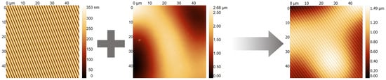
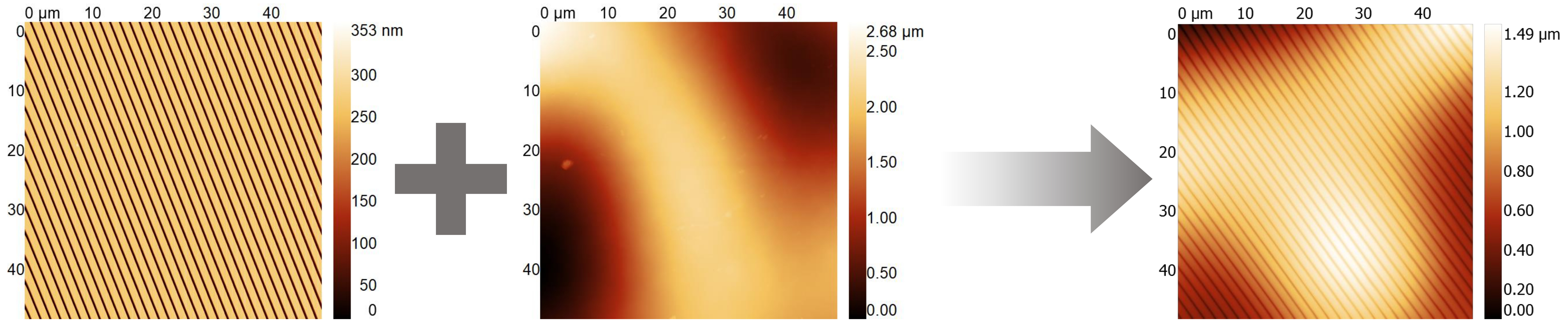
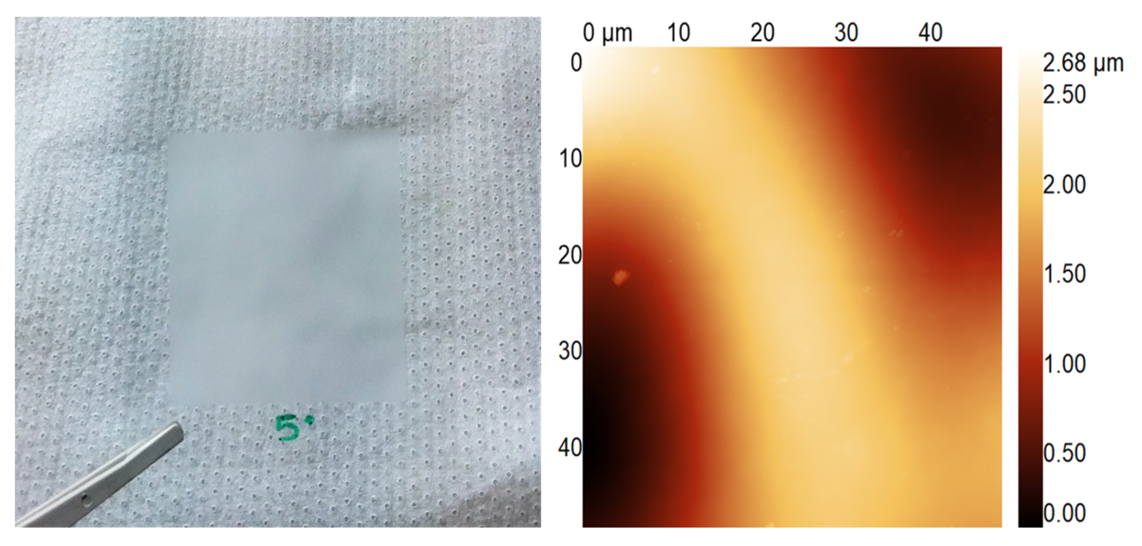
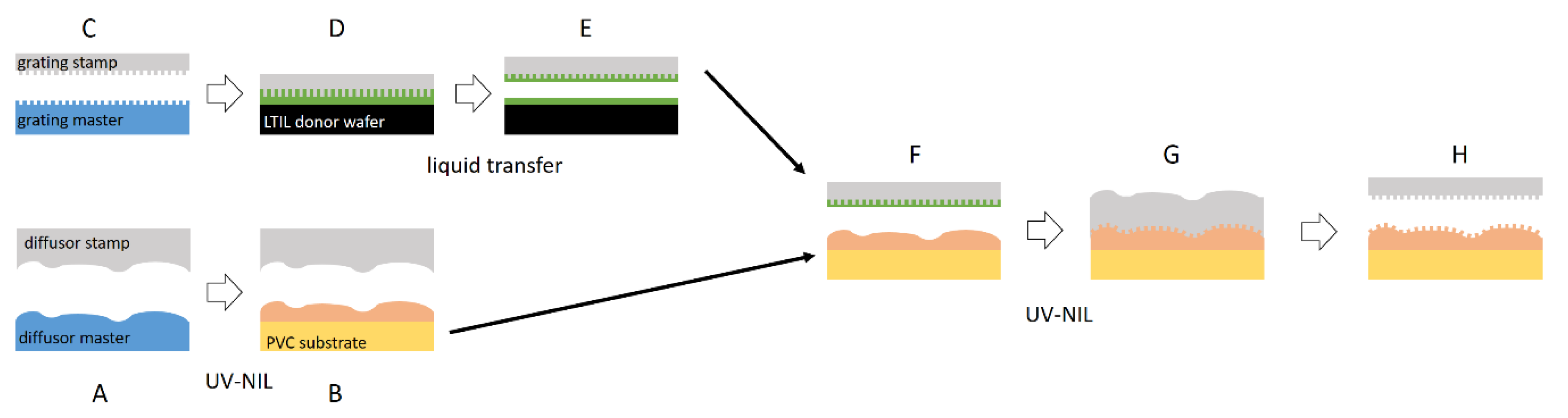
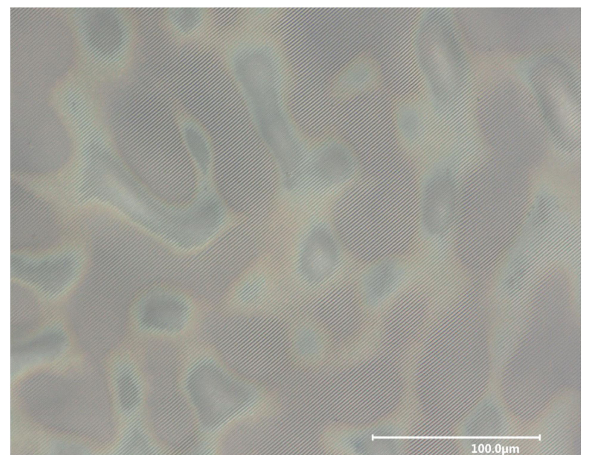
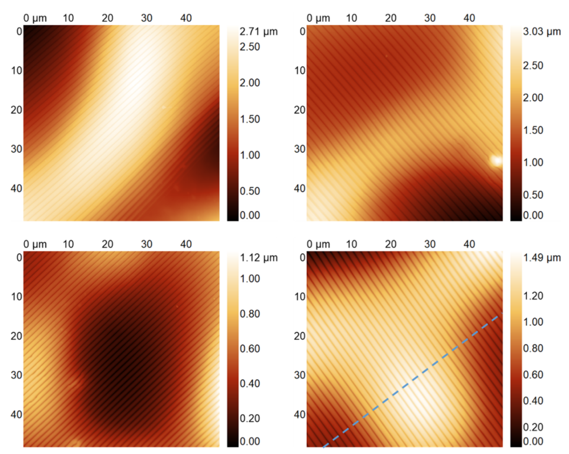
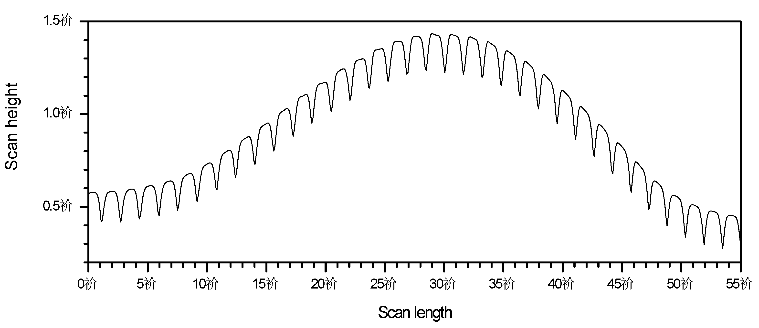
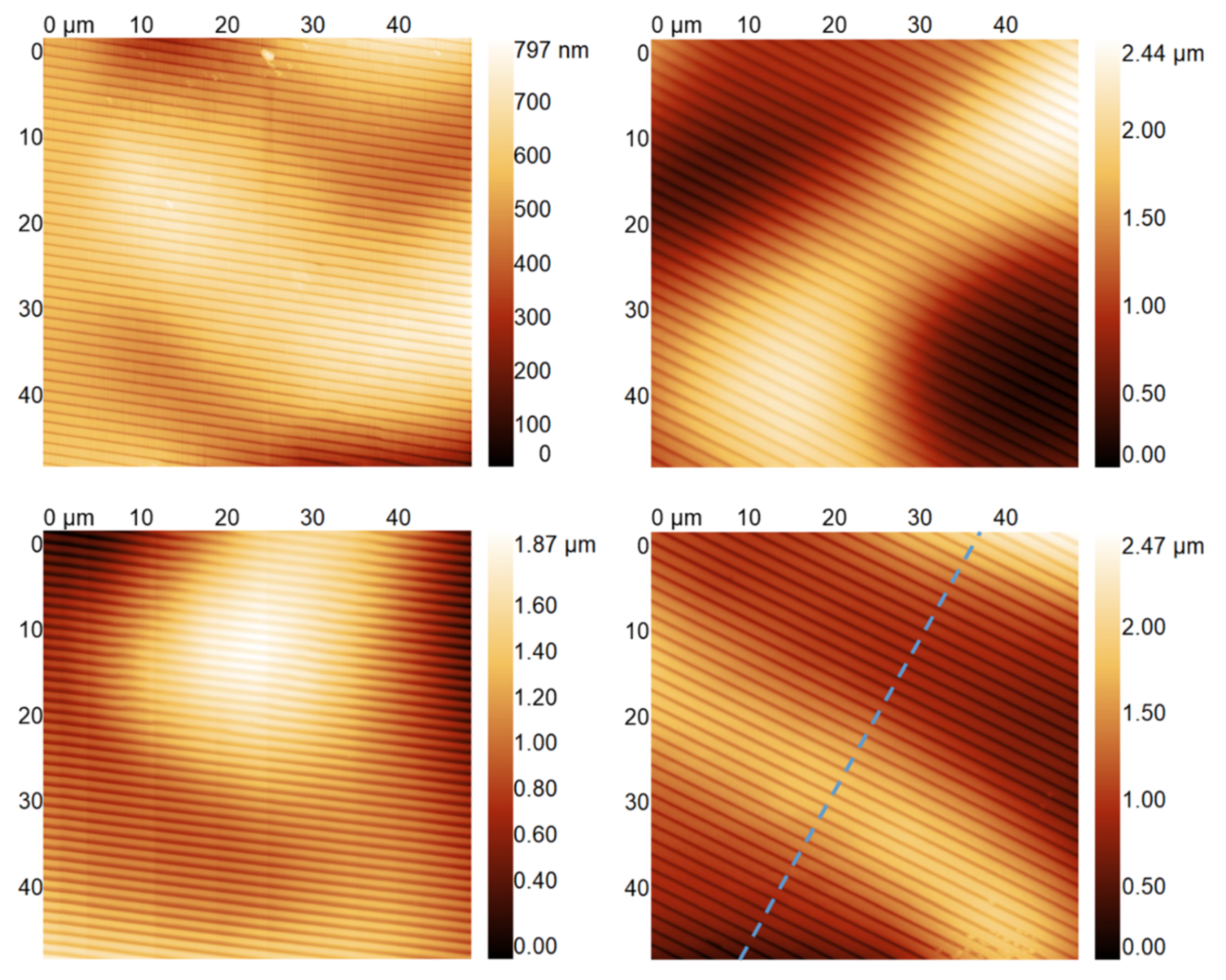
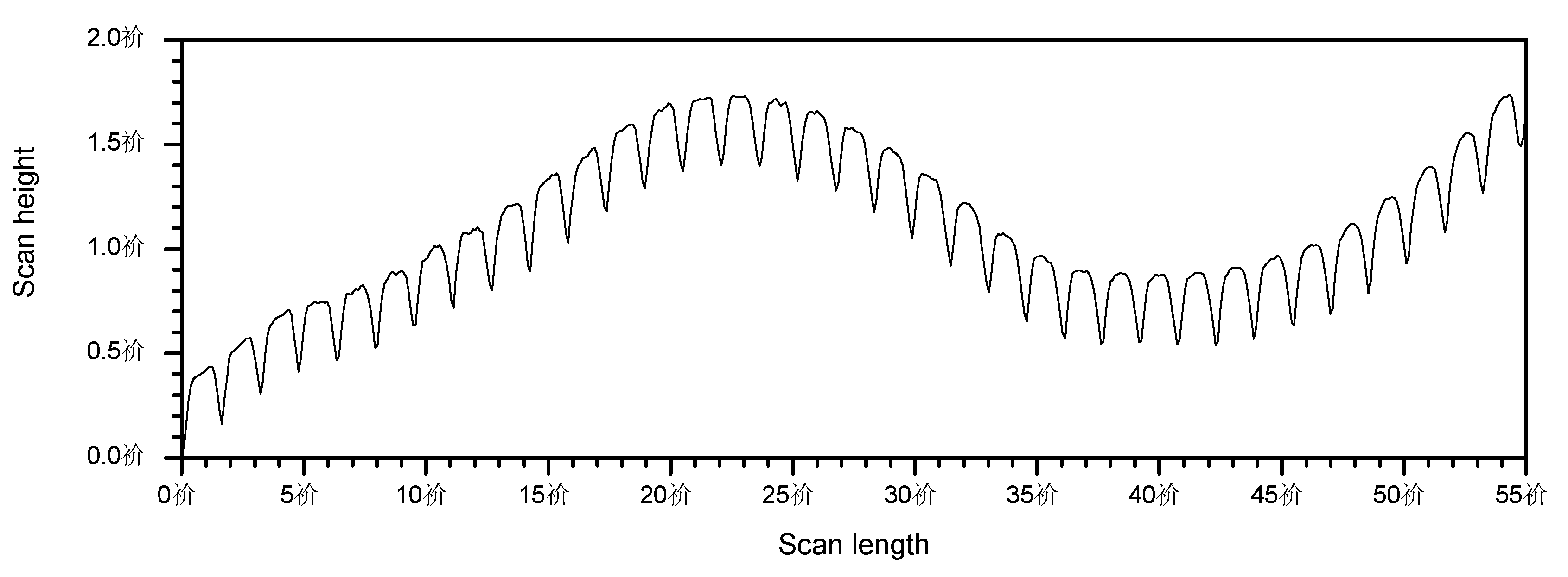
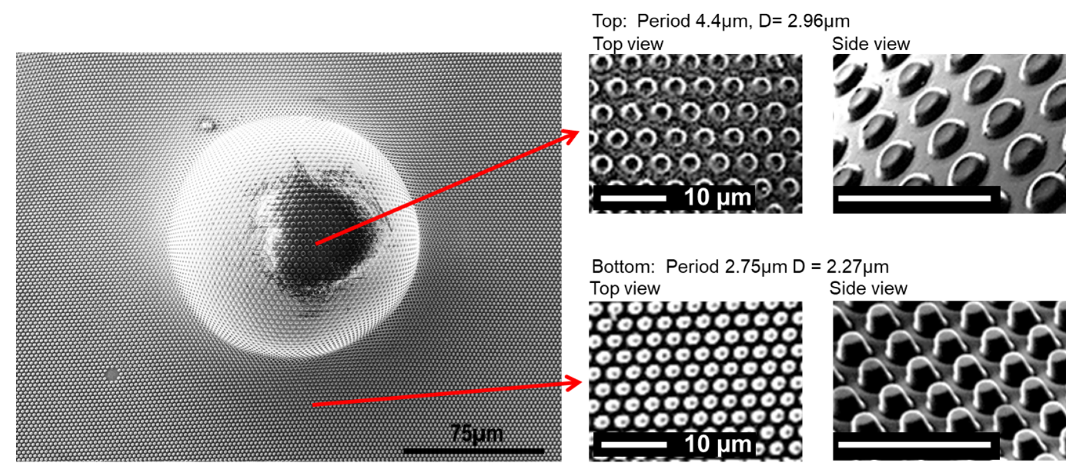
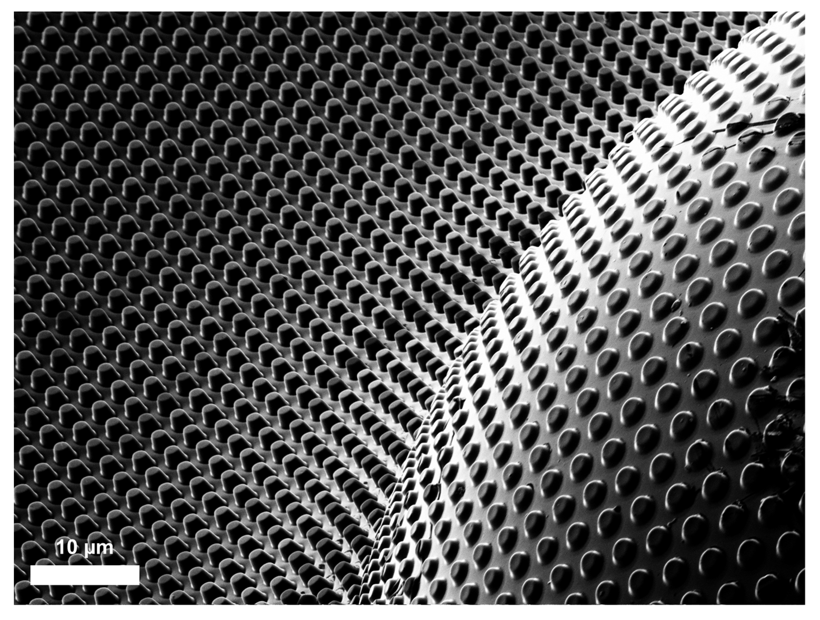
3.1. Hierarchical Stamp Master
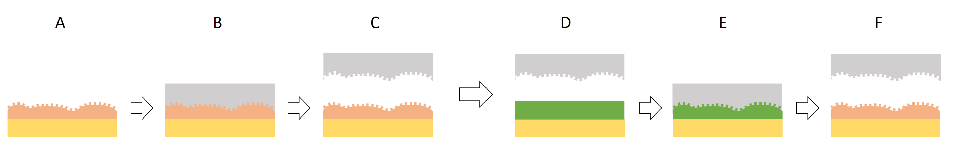
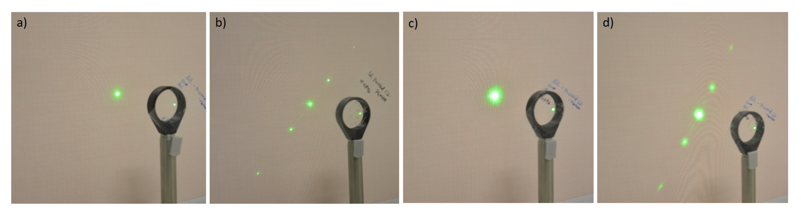
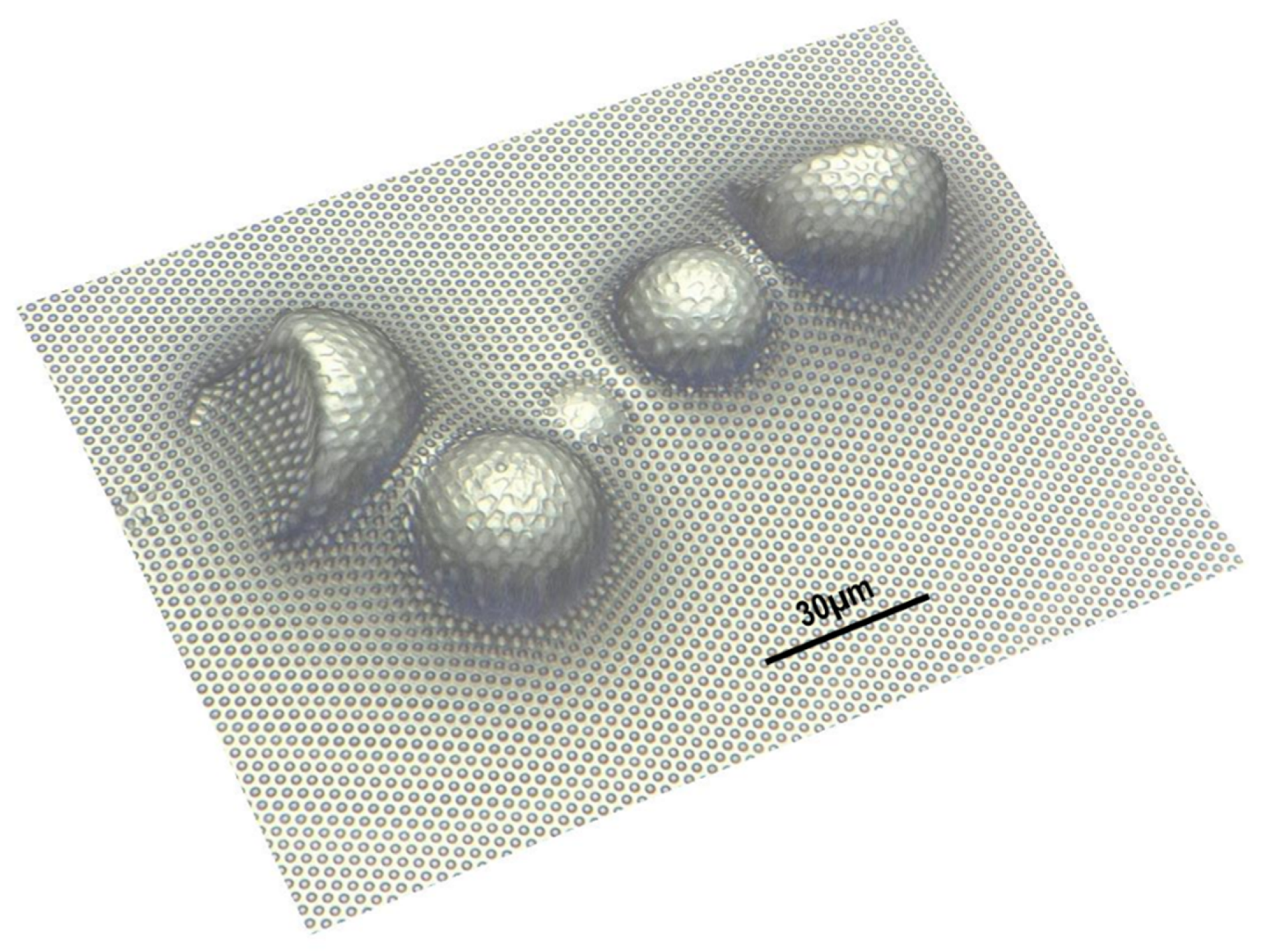
3.2. Direct Hierarchical Nanoimprint
4. Discussion
Author Contributions
Funding
Conflicts of Interest
Appendix A


References
- Schift, H. Nanoimprint lithography: An old story in modern times? A review. J. Vac. Sci. Technol. B Microelectron. Nanometer Struct. 2008, 26, 458. [Google Scholar] [CrossRef]
- Haisma, J. Mold-assisted nanolithography: A process for reliable pattern replication. J. Vac. Sci. Technol. B Microelectron. Nanometer Struct. 1996, 14, 4124. [Google Scholar] [CrossRef]
- Chen, Y.-P.; Lee, C.-H.; Wang, L.A. Fabrication and characterization of multi-scale microlens arrays with anti-reflection and diffusion properties. Nanotechnology 2011, 22, 215303. [Google Scholar] [CrossRef] [PubMed]
- Xie, S.; Wan, X.; Yang, B.; Zhang, W.; Wei, X.; Zhuang, S. Design and Fabrication of Wafer-Level Microlens Array with Moth-Eye Antireflective Nanostructures. Nanomaterials 2019, 9, 747. [Google Scholar] [CrossRef] [PubMed]
- Reboud, V.; Obieta, I.; Bilbao, L.; Saez-Martinez, V.; Brun, M.; Laulagnet, F.; Landis, S. Imprinted hydrogels for tunable hemispherical microlenses. Microelectron. Eng. 2013, 111, 189–192. [Google Scholar] [CrossRef]
- Glinsner, T.; Kreindl, G.; Kast, M. Nanoimprint Lithography: The technology makes its mark on CMOS image sensors and in the nano-world. Opt. Photonik 2010, 5, 42–45. [Google Scholar] [CrossRef]
- Kreindl, G.; Glinsner, T.; Miller, R.; Treiblmayr, D.; Födisch, R. High accuracy UV-nanoimprint lithography step-and-repeat master stamp fabrication for wafer level camera application. J. Vac. Sci. Technol. B Nanotechnol. Microelectron. Mater. Process. Meas. Phenom. 2010, 28, C6M57–C6M62. [Google Scholar] [CrossRef]
- Gale, M. Replication techniques for diffractive optical elements. Microelectron. Eng. 1997, 34, 321–339. [Google Scholar] [CrossRef]
- Gale, M.; Rossi, M.; Rudmann, H.; Saarinen, J.; Schnieper, M. Replicated diffreactive optical elements in consumer products. In Proceedings of the Diffractive Optics and Micro-Optics, Rochester, NY, USA, 10–13 October 2004; OSA Publishing: Washington, DC, USA. [Google Scholar]
- Osipov, V.; Doskolovich, L.L.; Bezus, E.A.; Drew, T.; Zhou, K.; Sawalha, K.; Swadener, G.; Wolffsohn, J.S.W. Application of nanoimprinting technique for fabrication of trifocal diffractive lens with sine-like radial profile. J. Biomed. Opt. 2015, 20, 025008. [Google Scholar] [CrossRef]
- Schleunitz, A.; Schift, H. Fabrication of 3D nanoimprint stamps with continuous reliefs using dose-modulated electron beam lithography and thermal reflow. J. Micromech. Microeng. 2010, 20, 095002. [Google Scholar] [CrossRef]
- Gilles, S.; Meier, M.; Prömpers, M.; van der Hart, A.; Kügeler, C.; Offenhäusser, A.; Mayer, D. UV nanoimprint lithography with rigid polymer molds. Microelectron. Eng. 2009, 86, 661–664. [Google Scholar] [CrossRef]
- Muehlberger, M.; Boehm, M.; Bergmair, I.; Chouiki, M.; Schoeftner, R.; Kreindl, G.; Kast, M.; Treiblmayr, D.; Glinsner, T.; Miller, R.; et al. Nanoimprint lithography from CHARPAN Tool exposed master stamps with 12.5nmhp. Microelectron. Eng. 2011, 88, 2070–2073. [Google Scholar] [CrossRef]
- Junarsa, I.; Nealey, P.F. Fabrication of masters for nanoimprint, step and flash, and soft lithography using hydrogen silsesquioxane and x-ray lithography. J. Vac. Sci. Technol. B Microelectron. Nanometer Struct. 2004, 22, 2685. [Google Scholar] [CrossRef]
- Zhang, X.; Huang, R.; Liu, K.; Kumar, A.S.; Shan, X. Rotating-tool diamond turning of Fresnel lenses on a roller mold for manufacturing of functional optical film. Precis. Eng. 2018, 51, 445–457. [Google Scholar] [CrossRef]
- Mühlberger, M.; Rohn, M.; Danzberger, J.; Sonntag, E.; Rank, A.; Schumm, L.; Kirchner, R.; Forsich, C.; Gorb, S.; Einwögerer, B.; et al. UV-NIL fabricated bio-inspired inlays for injection molding to influence the friction behavior of ceramic surfaces. Microelectron. Eng. 2015, 141, 140–144. [Google Scholar] [CrossRef]
- Neinhuis, C.; Barthlott, W. Characterization and distribution of water-repellent, self-cleaning plant surfaces. Ann. Bot. 1997, 79, 667–677. [Google Scholar] [CrossRef]
- Autumn, K.; Liang, Y.A.; Hsieh, S.T.; Zesch, W.; Chan, W.P.; Kenny, T.W.; Fearing, R.; Full, R.J. Adhesive force of a single gecko foot-hair. Nature 2000, 405, 681. [Google Scholar] [CrossRef]
- Gao, H.; Wang, X.; Yao, H.; Gorb, S.; Arzt, E. Mechanics of hierarchical adhesion structures of geckos. Mech. Mater. 2005, 37, 275–285. [Google Scholar] [CrossRef]
- Taillaert, D.; Bienstman, P.; Baets, R. Compact efficient broadband grating coupler for silicon-on-insulator waveguides. Opt. Lett. 2004, 29, 2749–2751. [Google Scholar] [CrossRef]
- Daubinger, R. Hierarchical Nanostructures for Energy Devices. Johns. Matthey Technol. Rev. 2016, 60, 151–157. [Google Scholar] [CrossRef]
- Li, W.-D.; Ding, F.; Hu, J.; Chou, S.Y. Three-dimensional cavity nanoantenna coupled plasmonic nanodots for ultrahigh and uniform surface-enhanced Raman scattering over large area. Opt. Express 2011, 19, 3925–3936. [Google Scholar] [CrossRef] [PubMed]
- Micro Resist Technology GmbH | Hybrid Polymers. Available online: https://www.microresist.de/en/product/hybrid-polymers (accessed on 27 February 2020).
- Huang, X.D.; Bao, L.-R.; Cheng, X.; Guo, L.J.; Pang, S.W.; Yee, A.F. Reversal imprinting by transferring polymer from mold to substrate. J. Vac. Sci. Technol. B Microelectron. Nanometer Struct. 2002, 20, 2872. [Google Scholar] [CrossRef]
- Koo, N.; Wuk Kim, J.; Otto, M.; Moormann, C.; Kurz, H. Liquid transfer imprint lithography: A new route to residual layer thickness control. J. Vac. Sci. Technol. B Microelectron. Nanometer Struct. 2011, 29, 06FC12. [Google Scholar] [CrossRef]
- Moormann, C.; Koo, N.; Kim, J.; Plachetka, U.; Schlachter, F.; Nowak, C. Liquid transfer nanoimprint replication on non-flat surfaces for optical applications. Microelectron. Eng. 2012, 100, 28–32. [Google Scholar] [CrossRef]
- Lee, J.; Park, H.-H.; Choi, K.-B.; Kim, G.; Lim, H. Fabrication of hybrid structures using UV roll-typed liquid transfer imprint lithography for large areas. Microelectron. Eng. 2014, 127, 72–76. [Google Scholar] [CrossRef]
- Uchida, T.; Yu, F.; Nihei, M.; Taniguchi, J. Fabrication of antireflection structures on the surface of optical lenses by using a liquid transfer imprint technique. Microelectron. Eng. 2016, 153, 43–47. [Google Scholar] [CrossRef]
- OrmoComp® | Micro Resist Technology GmbH. Available online: http://www.microresist.de/en/products/hybrid-polymers/uv-imprint-uv-moulding/ormocomp%C2%AE (accessed on 9 October 2017).
- Mühlberger, M.; Bergmair, I.; Klukowska, A.; Kolander, A.; Leichtfried, H.; Platzgummer, E.; Loeschner, H.; Ebm, C.; Grützner, G.; Schöftner, R. UV-NIL with working stamps made from Ormostamp. Microelectron. Eng. 2009, 86, 691–693. [Google Scholar] [CrossRef]
- Beschichtungen BGL-GZ-83 | PROFACTOR. Available online: https://www.profactor.at/loesungen/beschichtungen/ (accessed on 27 February 2020).
- Beschichtungen HMNP-12 | PROFACTOR. Available online: https://www.profactor.at/loesungen/beschichtungen/ (accessed on 27 February 2020).
- Köpplmayr, T.; Häusler, L.; Bergmair, I.; Mühlberger, M. Nanoimprint Lithography on curved surfaces prepared by fused deposition modelling. Surf. Topogr. Metrol. Prop. 2015, 3, 024003. [Google Scholar] [CrossRef]
- Toepke, M.W.; Beebe, D.J. PDMS absorption of small molecules and consequences in microfluidic applications. Lab. Chip 2006, 6, 1484. [Google Scholar] [CrossRef] [PubMed]
- Lamberti, A.; Marasso, S.L.; Cocuzza, M. PDMS membranes with tunable gas permeability for microfluidic applications. RSC Adv. 2012, 106, 61415–61419. [Google Scholar] [CrossRef]
- Nečas, D.; Klapetek, P. Gwyddion: An open-source software for SPM data analysis. Open Phys. 2012, 10, 181–188. [Google Scholar] [CrossRef]
- Haslinger, M.J.; Verschuuren, M.A.; van Brakel, R.; Danzberger, J.; Bergmair, I.; Mühlberger, M. Stamp degradation for high volume UV enhanced substrate conformal imprint lithography (UV-SCIL). Microelectron. Eng. 2016, 153, 66–70. [Google Scholar] [CrossRef]
- Haslinger, M.J.; Mitteramskogler, T.; Kopp, S.; Leichtfried, H.; Messerschmidt, M.; Thesen, M.W.; Mühlberger, M. Development of a Soft UV-NIL Step&Repeat and Lift-Off Process Chain for High Speed Metal Nanomesh Fabrication. Nanotechnology 2020, (in press).
- Schmitt, H.; Duempelmann, P.; Fader, R.; Rommel, M.; Bauer, A.J.; Frey, L.; Brehm, M.; Kraft, A. Life time evaluation of PDMS stamps for UV-enhanced substrate conformal imprint lithography. Microelectron. Eng. 2012, 98, 275–278. [Google Scholar] [CrossRef]
- Tucher, N.; Höhn, O.; Hauser, H.; Müller, C.; Bläsi, B. Characterizing the degradation of PDMS stamps in nanoimprint lithography. Microelectron. Eng. 2017, 180, 40–44. [Google Scholar] [CrossRef]
- Schmid, H.; Michel, B. Siloxane Polymers for High-Resolution, High-Accuracy Soft Lithography. Macromolecules 2000, 33, 3042–3049. [Google Scholar] [CrossRef]
- Pei, L.; Balls, A.; Tippets, C.; Abbott, J.; Linford, M.R.; Hu, J.; Madan, A.; Allred, D.D.; Vanfleet, R.R.; Davis, R.C. Polymer molded templates for nanostructured amorphous silicon photovoltaics. J. Vac. Sci. Technol. Vac. Surf. Films 2011, 29, 021017. [Google Scholar] [CrossRef]
- Verschuuren, M.A. Substrate Conformal Imprint Lithography for Nanophotonics. Ph.D. Thesis, Utrecht University, Utrecht, The Netherlands, 2010. [Google Scholar]
- Möllenbeck, S.; Bogdanski, N.; Scheer, H.-C.; Zajadacz, J.; Zimmer, K. Moulding of arrowhead structures. Microelectron. Eng. 2009, 86, 608–610. [Google Scholar] [CrossRef]
- Muehlberger, M. More than Just 2D: Nanoimprinting and Complex Geometries. In Proceedings of the 32nd International Microprocesses and Nanotechnology Conference (MNC 2019), Hiroshima, Japan, 28–31 October 2019. [Google Scholar]


© 2020 by the authors. Licensee MDPI, Basel, Switzerland. This article is an open access article distributed under the terms and conditions of the Creative Commons Attribution (CC BY) license (http://creativecommons.org/licenses/by/4.0/).
Share and Cite
Moharana, A.R.; Außerhuber, H.M.; Mitteramskogler, T.; Haslinger, M.J.; Mühlberger, M.M. Multilayer Nanoimprinting to Create Hierarchical Stamp Masters for Nanoimprinting of Optical Micro- and Nanostructures. Coatings 2020, 10, 301. https://doi.org/10.3390/coatings10030301
Moharana AR, Außerhuber HM, Mitteramskogler T, Haslinger MJ, Mühlberger MM. Multilayer Nanoimprinting to Create Hierarchical Stamp Masters for Nanoimprinting of Optical Micro- and Nanostructures. Coatings. 2020; 10(3):301. https://doi.org/10.3390/coatings10030301
Chicago/Turabian StyleMoharana, Amiya R., Helene M. Außerhuber, Tina Mitteramskogler, Michael J. Haslinger, and Michael M. Mühlberger. 2020. "Multilayer Nanoimprinting to Create Hierarchical Stamp Masters for Nanoimprinting of Optical Micro- and Nanostructures" Coatings 10, no. 3: 301. https://doi.org/10.3390/coatings10030301
APA StyleMoharana, A. R., Außerhuber, H. M., Mitteramskogler, T., Haslinger, M. J., & Mühlberger, M. M. (2020). Multilayer Nanoimprinting to Create Hierarchical Stamp Masters for Nanoimprinting of Optical Micro- and Nanostructures. Coatings, 10(3), 301. https://doi.org/10.3390/coatings10030301