


Abstract
The rapid adoption of Wide Band Gap (WBG) semiconductor technologies, particularly Silicon Carbide (SiC) and Gallium Nitride (GaN), together with emerging Ultra-Wide Band Gap (UWBG) materials such as AlGaN, Aluminum Nitride (AlN), Diamond, β-gallium oxide (β-Ga2O3), and Hexagonal Boron Nitride (h-BN), is reshaping wafer-level electrical testing beyond the capabilities of conventional silicon-based probing infrastructures. The increasingly demanding electrical, thermal, and mechanical operating conditions of these devices require probe cards to evolve from passive interconnects into integrated multiphysics systems capable of supporting high voltages, high current densities, and fast switching transients. This review analyzes the fundamental design constraints governing advanced probe card technologies, including probe-to-wafer contact physics, electrothermal behavior, insulation requirements, parasitic effects, and high-frequency performance. Particular attention is devoted to Vertical MEMS probe card architectures, which enable high contact density, low parasitic inductance, and improved current-carrying capability, making them particularly suitable for modern WBG applications. Emerging solutions, including ceramic insulation structures, controlled-atmosphere testing environments, integrated sensing, and advanced thermal management techniques, are also discussed. Furthermore, the paper examines the evolution of wafer-level testing strategies, from conventional parametric screening to reliability-oriented methodologies inspired by burn-in procedures, highlighting the growing importance of body-diode characterization for early defect detection in SiC devices. Beyond reviewing the current state of the art, this work proposes a structured taxonomy of probe card technologies and outlines a technology roadmap linking future WBG and UWBG device requirements with the evolution of wafer-level testing infrastructures.
1. Introduction
Wafer-level electrical testing is a dominant contributor to both manufacturing yield loss and overall cost of testing, accounting for approximately one third of total test cost for power semiconductor devices with full parametric and reliability screening. In many advanced manufacturing flows, test-related expenses consume a growing share of total production costs, with estimates reaching or exceeding 25–30% that are no longer outliers. This economic drag disproportionately affects high-volume consumer markets where margins are thin. Furthermore, test scalability is throttled by physical and logistical constraints, including limited test pin availability, thermal power envelope restrictions, and interface instability at high frequencies [1]. The probe card, acting as a space-transforming contact interface, represents the most stressed element of the test cell, serving as the electrical, thermal, and mechanical interface between the Automated Test Equipment (ATE) and the device under test (DUT).
Conventional semiconductor ATE infrastructures were historically fine-tuned for silicon technologies operating below hundreds of volts. However, new WBG and UWBG devices, such as commercial GaN HEMTs, are designed with a breakdown voltage (BV) much higher than the rated voltage to provide a large overvoltage margin in converter applications. The dynamic BV of a 650 V rated GaN HEMT under 25 ns pulses (dv/dt > 100 V/ns) was found to be over 1400 V [2]. In addition, SiC switching devices with blocking voltages up to 1.2 kV, specific on-resistances as low as 5 mΩ·cm2, and current ratings exceeding 20 A have been reported in Table 1 of the study cited in [3]. These operating conditions place significant demands on wafer-level test infrastructures, requiring high-voltage isolation, minimized parasitic impedance, and accurate dynamic characterization capabilities. Accordingly, wafer-level characterization beyond 1.5–3 kV becomes increasingly constrained by probe card and test platform limitations, thereby requiring dedicated insulation architectures, specialized high-voltage interfaces, and external high-voltage instrumentation. The industry suffers significantly from the conventional probe card, in which tens to hundreds of cantilever needles are manually mounted onto an epoxy ring. Continually increasing pad density and narrowing pad pitch would soon break the limit of manual assembly ability. Crosstalk and parasitic inductance also make epoxy probe cards difficult for high-speed testing. Additionally, the conventional metal needles tend to be deformed under hundreds of touchdowns, and the calibration process is time-consuming. To solve these problems, several attempts have been made to seek a substitute based on advanced microelectromechanical systems (MEMS) technologies [4]. In silicon technologies, probing environments were historically limited to DC voltages below 800 V, maximum currents below 2 A per pin, and pad pitches ≥ 60 µm.
Table 1.
Comparison between cantilever and vertical probing technologies for HC-HV wafer testing.
These conditions allowed the use of cantilever-based or hybrid probe technologies with modest electrical optimization. In contrast, Wide Band Gap power devices introduce constraints exceeding conventional probe card capabilities. As reported in [5], WBG materials have a wide energy bandgap, above 3 eV, which leads to a large breakdown electric field of about 3 MV/cm, 10 times higher than that of silicon. At present, SiC is used in high-voltage power transistors, covering several voltage classes: 650 V, 900 V, 1000 V, 1200 V, and 1700 V [5]. On-state current densities exceeding 500–1000 A/cm are shown in [6], and in more complex devices, GaN on SiC Trench MOSFETs [7]. While the intrinsic semiconductor material of Silicon Carbide (SiC) can theoretically withstand junction temperatures (Tj) exceeding 300 °C, the maximum operating junction temperature for mass-produced commercial SiC power devices is practically limited by packaging and interconnect materials. As reported in [8], the maximum operating temperature is 200 °C; this heightened temperature exacerbates the likelihood of insulation damage, an area that has unfortunately received limited attention in existing literature. GaN, instead, covers a wide voltage range, from 15 to 1200 V [6]. GaN HEMTs, conversely, are characterized by very low intrinsic device capacitances, switching frequencies corresponding to effective bandwidths in the hundreds of megahertz, and dv/dt values routinely exceeding 100 V/ns. These figures push wafer-level probing well beyond traditional design envelopes, exposing hard limits in contact resistance stability, parasitic inductance and loop area, dielectric spacing and surface discharge behavior, and local thermal dissipation at the probe tip. As a result, probe card development has shifted toward a system-level co-design paradigm, integrating Vertical MEMS probe architectures, multilayer space transformers, Kelvin sensing, and controlled electromagnetic routing as standard practice in WBG test environments. The contribution of this paper is therefore not the introduction of a new probe card architecture, but the development of a technology-oriented roadmap that links device-level requirements to probe card design constraints and industrial testing strategies.
The paper provides three main contributions. First, it proposes a structured taxonomy of probe card technologies, comparing conventional cantilever, MEMS, vertical, and vertical MEMS solutions with respect to the electrical, thermal, and mechanical requirements imposed by testing modern SiC and GaN devices. Second, it consolidates quantitative performance indicators reported across the literature, including current density capability, contact resistance, parasitic inductance, thermal limitations, insulation requirements, and high-voltage operating constraints. Third, it discusses how these requirements evolve across various stages of the industrial test flow, from wafer-level screening to medium-parallelism characterization and Known-Good-Die (KGD) validation, thereby providing a roadmap for future probe card development in the context of WBG and UWBG semiconductor technologies.
2. Vertical Probe Card Architectures
A wafer-level testing probe card is utilized as the principal interface for signal routing to the ATE, to pass or fail the DUT [4]. The most commonly used probe card can be classified into Cantilever or Epoxy probe cards, MEMS probe cards, Vertical probe cards and Vertical MEMS probe cards. The conventional Epoxy-type probe card consists of a PCB (printed circuit board) that supports an array of delicate wire contacts. These contacts serve as the electromechanical interface between the device under test, so-called DUT, and the test electronics [9]. Even if this solution was the first testing system used and it is currently the most common and cheapest solution, it has several limitations discussed in [4], such as: probing force that exceeds 10 g/probe, uniform probing forces (since the probe deflection was nonuniform across the membrane), large pitch greater than 100 µm, pin counts lower than some hundreds, deep scrub marks, high resistance and high inductance path. All these characteristics limit the application field. A novel silicon probe card using a MEMS process to solve the limitations of fine pitch, high frequency, and the problem of the silicon process for probe cards is designed. This probe is applicable to fine pitches of less than 50 µm, forces of less than 5 g, and frequencies of more than 2 GHz [9].
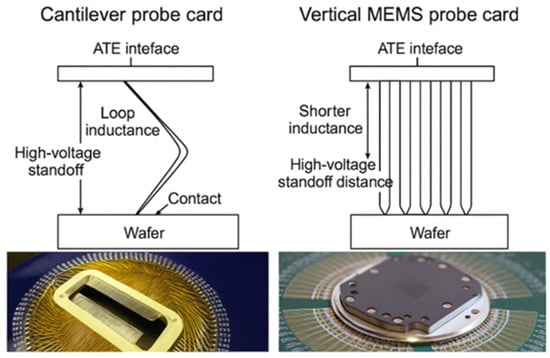
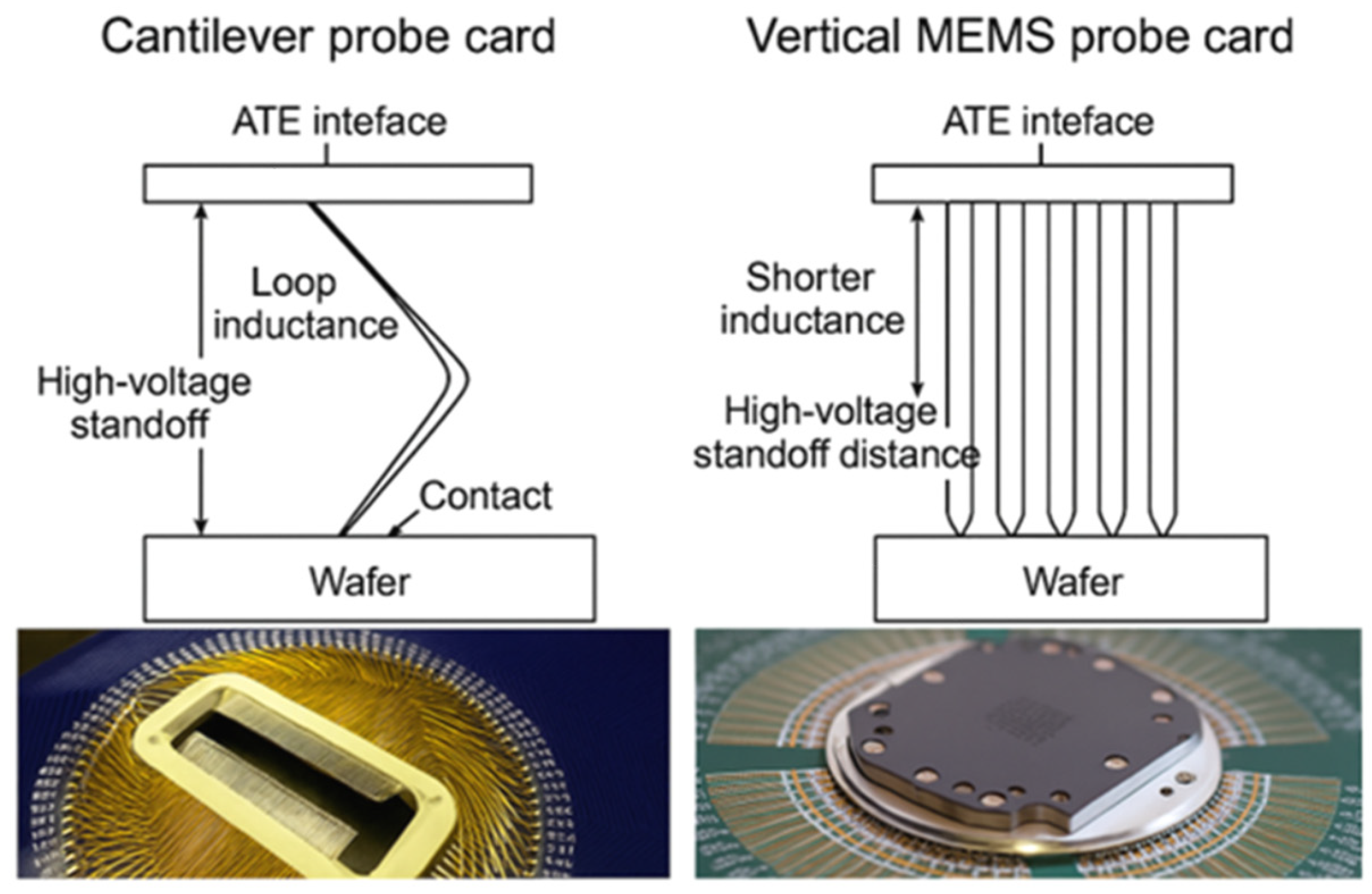
Today’s ATE is not well suited to adapting to a MEMS probe card because it is more fragile than an epoxy solution. Vertical probe card architectures were introduced to overcome these constraints by re-engineering the probe-to-tester interconnect as a compact, symmetric, and scalable three-dimensional system. Unlike cantilever solutions, Vertical probe cards orient probe elements orthogonally to the wafer surface and integrate them into multilayer redistribution structures, commonly referred to as space transformers. It appears to be a pivotal technology for testing these densely packed semiconductor wafers, enabling precise contact with microprobes that traditional cantilever probe cards cannot adequately address. Vertical probes are radially arranged and mounted on an epoxy ring or other substrate. They are shorter than cantilever types, especially when manufactured using MEMS technology, reducing contact pressure and resistance. Figure 1 illustrates the conceptual architectural differences between Cantilever-based and Vertical probe card solutions.
Figure 1.
Conceptual and practical comparison between conventional cantilever probe cards and vertical probe card architectures. The upper diagrams illustrate the differences in current-loop length, parasitic inductance, and high-voltage standoff capability. The lower photographs show representative examples of both technologies: a cantilever probe card, characterized by a central keep-out area caused by the radial arrangement of probe needles, and a vertical probe card architecture, which enables a more compact and uniform probe distribution across the device surface. Image courtesy of Technoprobe S.p.A.
Today, Vertical probe cards with cost-effectiveness are generally selected for high-end SOC wafer test [10]. The transition from silicon to Wide Band Gap power devices fundamentally alters the physical and electrical requirements imposed on wafer-level probing. Conventional cantilever-based probe cards, historically customized for moderate voltage, current, and switching speed, encounter intrinsic limitations when applied to SiC and GaN technologies. These limitations arise primarily from extended current loop geometries, insufficient control of parasitic inductance, and inadequate dielectric spacing under multi-kilovolt stress. By minimizing electrical path length and loop area, vertical architectures significantly reduce parasitic inductance, typically achieving 1–3 nH per probe channel, compared to 5–15 nH commonly observed in cantilever solutions. This reduction is critical for dynamic WBG measurements, where high di/dt values can produce substantial voltage overshoot and waveform distortion. Furthermore, the vertical geometry naturally improves symmetry between force application, current conduction, and electric-field distribution, reducing localized stress concentrations at the probe-to-pad interface.
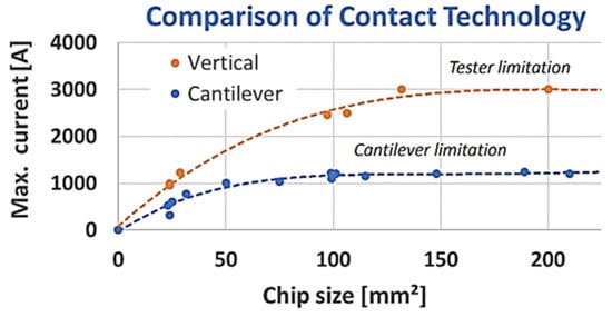
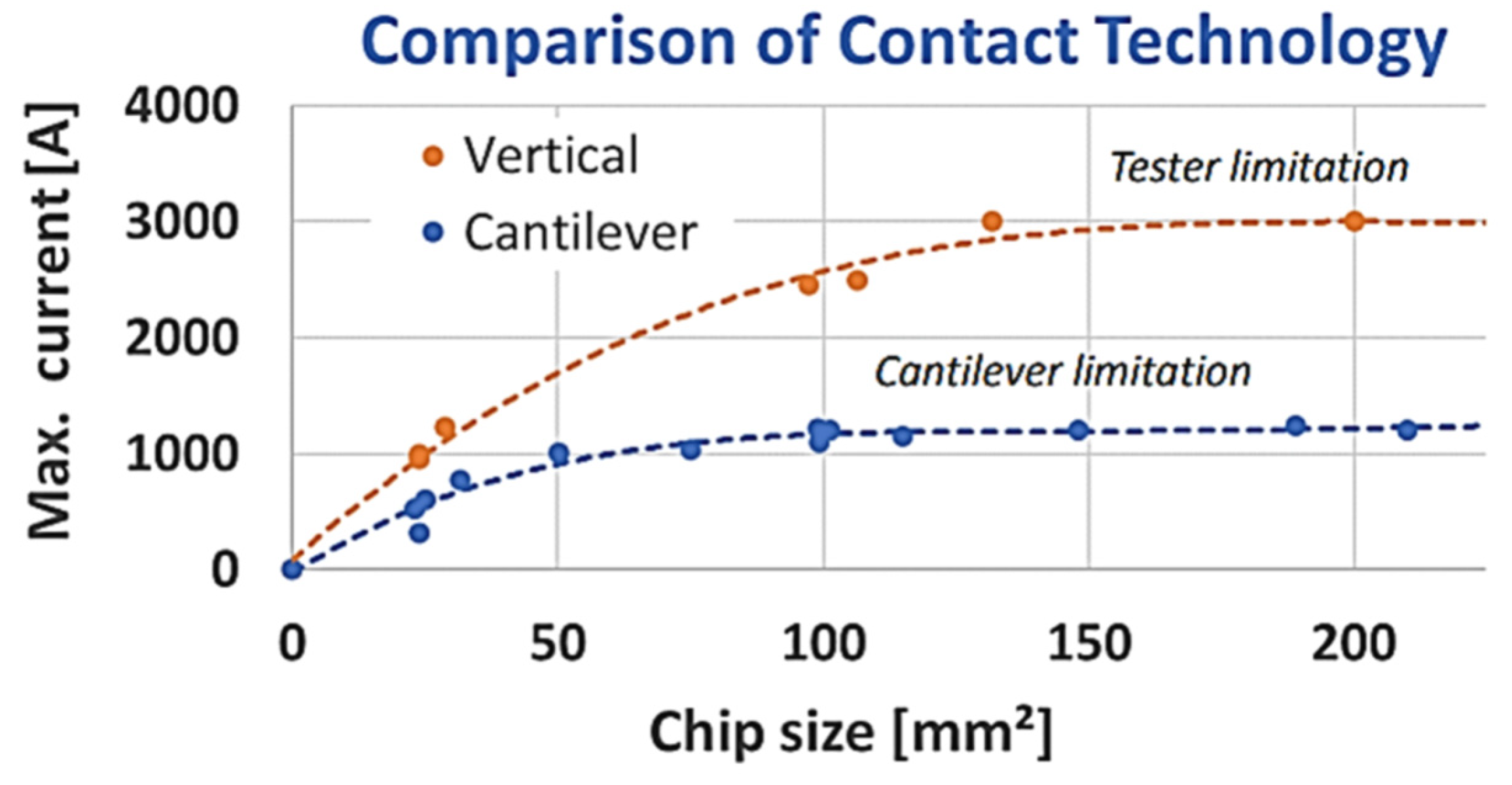
As described in [11], vertical probes technology has an inherent advantage in terms of current density. A factor of 1.7 is already achieved for small devices. For larger devices, physical constraints related to cantilever needle spiders further increase the advantage of vertical technology. While vertical probe heads can access the entire chip surface, cantilever technology is limited to a maximum number of probe layers, creating a “blind spot” in the center. This behavior and the improved wafer accessibility are quantitatively illustrated in Figure 2. Overall, the maximum current of 3000 A is related to tester limitations.
Figure 2.
Comparison of probe contact technologies showing the higher current-density capability and improved wafer accessibility offered by vertical probing architectures. Adapted from [11].
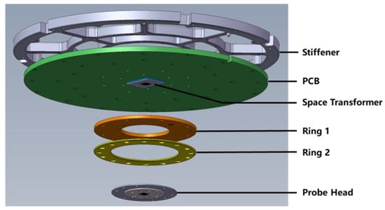
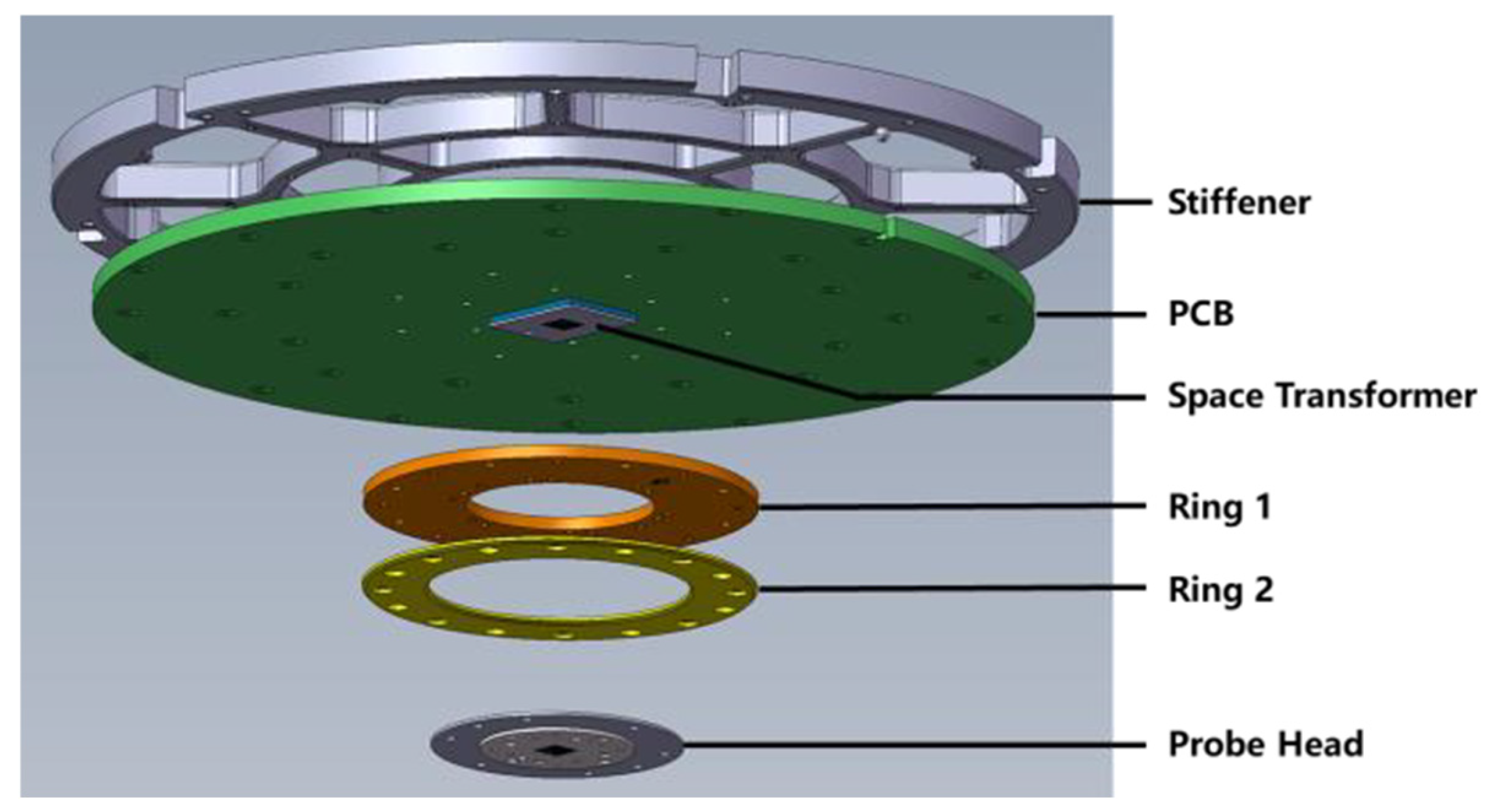
The intrinsic complexity of vertical probe cards is best understood by examining their internal mechanical and electrical composition. Figure 3 shows an exploded view of a representative Vertical probe card with Space Transformer (ST) assembly. It is composed of a PCB, ST, probe head, and certain mechanical parts (stiffener, ring 1, and ring 2). The stiffener is used to fix the PCB, while ring 1 and ring 2 are used to fix the probe head.
Figure 3.
Exploded view of a representative vertical probe card architecture, highlighting the probe head, multilayer space transformer (ST), printed circuit board (PCB), mechanical support rings, and stiffening structures. Reproduced from [10].
The role of the ST is to fan out the probe points from a small pitch to a large pitch. ST is the difficulty and key point of vertical probe card design and manufacture. This is mainly because with the rapid development of integrated circuits, the array of wafer pins is getting larger and the pitch is getting smaller. Among them, the PIN scale of high-end SOC products reaches 4000~5000 pins, and the pitch reaches 80~150 μm. This brings great challenges to the design and manufacture of ST [10]. Figure 3 illustrates the hierarchical organization of the probing system and the central role of the ST in redistributing high-current-density probe arrays toward the larger pitch required by the ATE.
The mechanical robustness and scalability of vertical architectures further enable compatibility with increasing wafer diameters and higher test parallelism. Starting from [12], a comparative table between the cantilever solution versus vertical solution for High Voltage (HV) and High Current (HC) is summarized, and it is shown in Table 1.
2.1. Probe Card as a Multi-Physics System
A modern probe card must be treated as a strongly coupled electro-thermal-mechanical system, where second-order effects become first-order error sources under WBG operating conditions.
2.1.1. Electrical Domain
Signal path resistance is the total resistance from the bond pad to the tester, i.e., the total of the contact, probe, solder connection, trace, and pogo/pin interconnect resistances.
A contact resistance of less than 1 Ω is desirable, although the actual acceptable value depends upon the application [4,13]. For example, the contact resistance between the tungsten probe and the copper foil is approximately 100 mΩ and becomes stable at an overdrive of 45 μm. However, contact resistance increases with an increasing number of contacts. In general, the probe should be removed for cleaning following 30,000 contacts to ensure that a contact resistance of less than 1 Ω is maintained [13].
Probe contact resistance (Cres) has become increasingly important as signal voltages drop, contact pressures decrease, and new devices based on technologies like gallium arsenide draw higher currents. Signal integrity has become even more dependent on probe contact quality. Cres is the interface resistance between the probe tip and the bond pad at overdrive. It is a function of the pad material, contact force, probe material, tip diameter, and tip shape [14]. Several new developments show that MEMS solutions reduce the Cres to about 0.4 Ω [15]. Typical parasitic inductance in probe cards depends on probe geometry and current loop length. Cantilever probes, due to their longer and inclined structure, exhibit self-inductance approximately four times bigger than vertical MEMS probes, with shorter and more compact paths, achieving lower values of less than 5 nH, with measurements close to ~0.14 nH reported [16], and 2 nH reported in [17]. Otherwise, parasitic capacitance stays in the order of 50–200 fF per channel for both architectures, as it is governed by probe pitch and dielectric environment, leading to only limited reduction in vertical designs compared to cantilever implementations.
2.1.2. Contact Physics and Resistance Evolution
According to a FormFactor study reported in [18], contact resistance is primarily governed by probe deflection and contact force. Therefore, variations in overdrive and the resulting contact force directly affect the total resistance of the electrical path. At the probe-to-pad interface, the true electrical contact area is typically less than 1% of the apparent contact footprint and is governed by asperity-level deformation mechanisms. For gold- or rhodium-based probe tips contacting aluminum or copper pads, typical contact forces range from 1 gf to 5 gf [19]. The experimental results described in [20] show that, when applying an overdrive within 100 µm to different vertical probe lengths, the maximum force is 3 gf. For these cases, it is assumed that the initial contact resistance is approximately 0.4 Ω at 50 µm overdrive [13]. Over the probe lifetime, contact resistance generally increases, reaching values two to five times higher after 105–106 touchdowns. Under high-current stress, localized Joule heating occurs at the micro-contact spots where current constriction is maximum. Even when the wafer chuck temperature is controlled between 25 °C and 125 °C, local temperatures at the probe-to-pad interface can exceed 150–250 °C [21]. These conditions promote oxide growth, material transfer, micro-welding phenomena, and pad damage, making contact resistance a time- and history-dependent parameter.
2.1.3. Mechanical and Thermal Coupling
In MEMS probe cards, probe performance is governed by a strong coupling between thermal and mechanical effects. As current flows through the probe, Joule heating increases its temperature, which alters material properties such as stiffness and yield strength, thereby affecting contact force, stress distribution, and deformation behavior. In addition, mechanical deformation is not limited to the probe itself but involves the interaction between the probe and the contacted wafer structures, including solder balls, Cu pillars, and TSVs. Finite element analyses have demonstrated that, during touchdown and overdrive, both the probe and the interconnect structures experience coupled deformation and stress evolution, which directly affect contact mechanics and reliability [22]. Moreover, the mechanical response of the probe is strongly influenced by its geometry and its integration within the probe card structure, as boundary conditions and mounting configurations can significantly modify stress levels and contact forces during probing [23]. As widely discussed in [24], during the wafer testing process, the wafer can reach temperatures in the range of 40 to 200 °C. Probes are the most thermally stressed components of a probe card, as they are simultaneously exposed to wafer heat and to self-heating caused by Joule losses. The highest temperatures are typically reached near the central section of each probe. Thermal management is further challenged by the closed architecture of the Probe Head, where densely packed probes have limited exposure to the external environment, reducing heat dissipation efficiency. Under particularly demanding operating conditions, forced-air cooling systems may be employed to enhance heat removal. Consequently, the development of advanced probe alloys with improved thermal, electrical, and mechanical properties remains a key research area for Probe Card manufacturers [24].
Probe bending (buckling) plays a key role in regulating the contact force, while localized plastic deformation may occur within the interconnect structures, directly affecting electrical contact quality and long-term reliability. The results discussed in [22], show that incorporating Au layers within a NiCo probe reduces electrical resistivity and temperature rise, improving current-carrying capacity while simultaneously lowering contact forces and minimizing interconnect deformation. However, due to the lower yield strength of gold, this design introduces a trade-off between enhanced electro-thermal performance and reduced mechanical durability under repeated loading cycles.
2.2. Signal and Power Integrity Limitations
In advanced WBG device testing, power distribution network (PDN) behavior of the probe card becomes a first-order design constraint rather than a post-layout verification concern. PDN analysis, in high-voltage and high-current probe cards, is to ensure that electrical power is delivered from the ATE to the DUT with sufficient voltage stability, minimal power loss, controlled current distribution, and acceptable thermal performance [24].
Kim et al., in [25], demonstrated that the power integrity of probe cards is strongly influenced by the design of the Space Transformer power distribution network. Through impedance analysis and time-domain simulations, they showed that optimized power/ground planes combined with properly placed decoupling capacitors significantly reduce power impedance, resonance effects, and simultaneous switching noise, thereby improving the electrical stability of high-density wafer testing systems [25]. Integrating PDN impedance extraction with electrothermal simulation provides valuable insight into both electrical and thermal behavior.
An example of this approach was presented by Li et al. [26], who developed a finite-element-method (FEM) electrothermal co-simulation framework for PDN analysis, investigating not only voltage-noise phenomena but also the simultaneously switching noise (SSN)-induced self-heating effects at each frequency point. Their results showed that conductor and dielectric losses within the PDN directly contribute to the temperature rise in the structure [26]. Although originally developed for IC power-delivery networks, the same electrothermal methodology can be extended to probe-card models, where parasitic impedance, current crowding, and power dissipation may generate localized hot spots during high-power WBG testing. Therefore, PDN characterization can support not only signal- and power-integrity verification but also predictive thermal management and test-duty-cycle optimization.
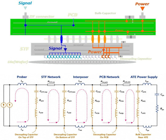
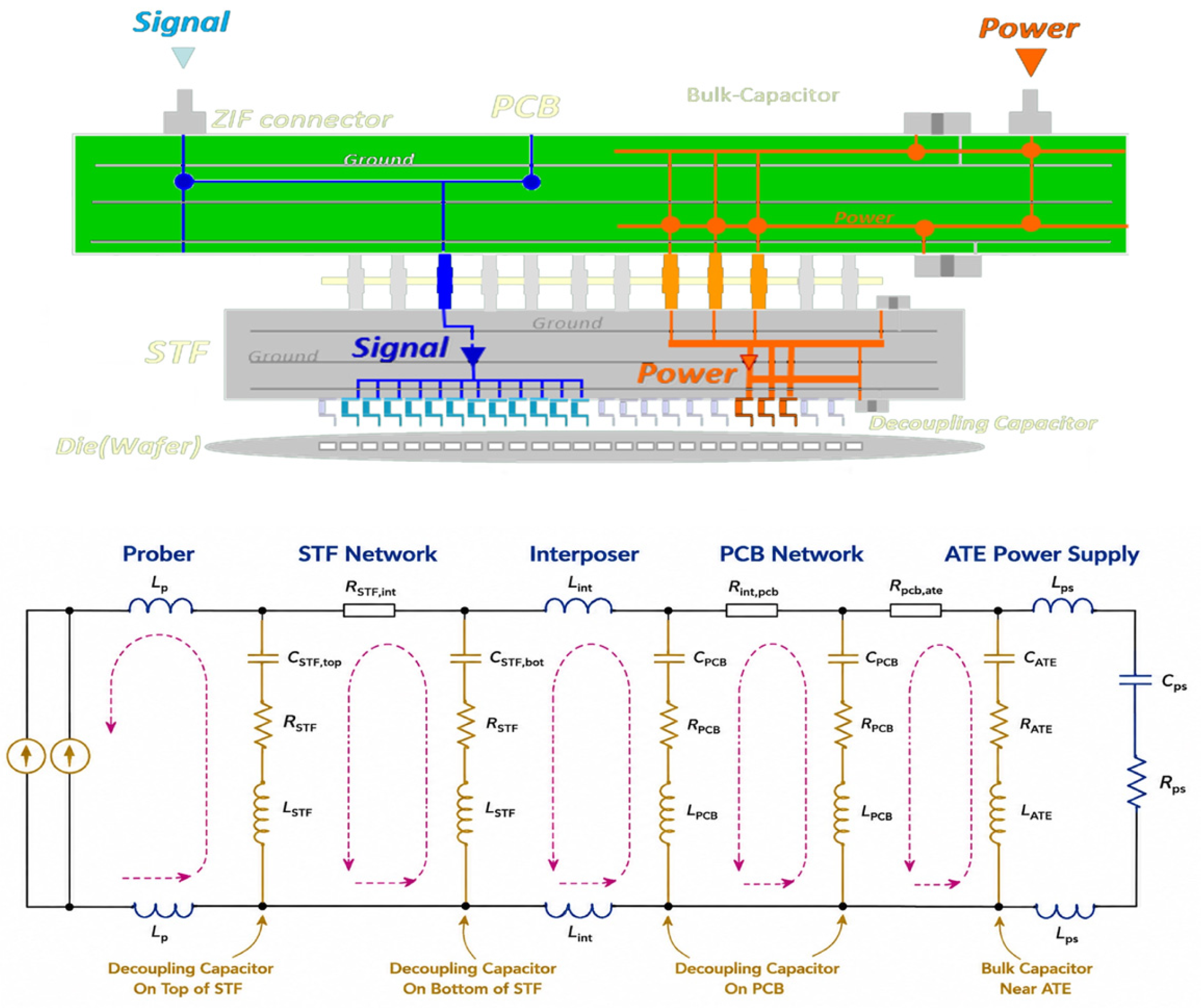
KT Kyun et al. in [25], introduced an equivalent RLC model of the probe card to enable accurate simulation of PDN behavior during wafer-level measurements. In this model, shown in Figure 4, the probe card is represented by a distributed network of parasitic resistances (R), inductances (L), and capacitances (C), which capture the electrical behavior of the signal paths, contact interfaces, and return current paths. This equivalent circuit is essential for reproducing realistic transient and frequency-dependent effects introduced by the probing system, which can significantly distort PDN characterization if neglected. By incorporating the probe card RLC model into PDN simulations, it becomes possible to predict voltage drop more accurately, resonance phenomena, and current delivery limitations, thereby improving correlation between simulation results and measured data at wafer level.
Figure 4.
Power delivery of probe card and equivalent RLC circuit model used for PDN analysis. Reproduced from [25].
3. Wide Band Gap Device Testing Challenges
SiC wafer probing routinely requires blocking voltage verification at 1.2 kV, 1.7 kV [5], and 3.3 kV, with emerging technologies extending toward 6.5 kV [27]. Electric-field management below 0.2–0.3 MV/cm along probe card surfaces is essential to prevent partial discharge inception, particularly in air or nitrogen environments. DUT pads are separated by a gap of hundreds of microns, and if the test is performed in air at room temperature and exhibits a voltage drop exceeding 500–600 V, ionization phenomena and consequently arc can occur, causing irreversible damage to the DUT, the PC and/or the entire test equipment too [27]. At the probe-to-pad interface, effective current densities can exceed 105–106 A/cm2, resulting in contact hot-spot formation, accelerated wear, and probe metal recrystallization. WBG devices working with dv/dt > 100 V/ns amplify the impact of every parasitic element in the test path. In this regime, loop inductance reduction below 2 nH is no longer optional but mandatory for accurate dynamic characterization [28].
Standard tester load boards and pogo-based interfaces are not designed for continuous operation above 1.5–3 kV, leading to partial discharge inception and long-term insulation degradation. Furthermore, WBG testing often requires tens to hundreds of amperes per site, with transient current slew rates exceeding kA/µs, far beyond the PDN capability of conventional ATE channels. Thermal instability adds an additional constraint: the ATE–prober–probe card stack is not thermally symmetric, and without coordinated redesign, localized temperature drift leads to parametric instability and reduced test repeatability.
Therefore, testing WBG devices without upgrading the probe card concept and entire ATE ecosystem results in systematic measurement errors, yield loss, and accelerated hardware degradation.
The trends clearly show that high-voltage wafer-level testing of WBG devices is driving a transition toward Vertical MEMS probe card architectures, which remain the primary enabler for low-inductance and high-parallelism probing. Ceramic-based structures are increasingly adopted in high-voltage probe card design due to their high dielectric strength, low permittivity, and thermal stability. These materials enable improved electric field control, reduced risk of surface discharge, and enhanced mechanical robustness under thermal cycling conditions, as reported in recent industrial contributions. In [27] (paragraph III, section B), a novel system named MCP is used to uniformly distribute current per needle and to mitigate the hot temperature point phenomena inside the probe head during the test. This technology is protected by [29,30], Technoprobe patents.
In parallel, high-voltage probing is increasingly performed in controlled environments to suppress partial discharge and arc formation.
Schmidt et al., in [31], proposed a high-voltage wafer-level probing environment based on a pressurized chamber concept, enabling operation in accordance with Paschen’s law to increase dielectric strength and minimize the risk of electrical arcing during testing.
The system integrates a full-wafer contactor designed for fast high-voltage characterization of HV IGBTs and diodes, significantly accelerating the development of new power device designs. It supports a wide temperature range from −40 °C to 175 °C and allows, within a lossless pressure vessel, the use of insulating gases (e.g., SF6) for demanding high-voltage applications.
Experimental results further prove extremely low parasitic leakage currents down to approximately 1 nA at 10 kV, confirming the suitability of the setup for high-precision characterization under extreme electrical and thermal stress conditions.
4. Industrial Implementation and Advanced Probe Card Technologies
Wafer-level testing forms the first and most comprehensive screening stage, enabling electrical characterization across the entire wafer before singulation. Unlike selective testing approaches, it maximizes die coverage and allows early identification of manufacturing defects, thereby improving overall yield. For WBG technologies, wafer-level testing is increasingly extended beyond basic parametric measurements to include reliability-oriented stress screening methodologies, conceptually like burn-in procedures. In particular, the evaluation of the intrinsic body diode in SiC MOSFETs has become a widely adopted technique, as forward-conduction and leakage-current measurements can rapidly reveal crystal defects, dislocations, and process-related anomalies. Implementing these tests requires advanced probe card architectures capable of supporting simultaneous high-voltage and moderate-to-high current operation over many contact points.
Key requirements include MEMS-based vertical probes for dense pad access, high-voltage insulation structures, Kelvin sensing techniques for correct low-current measurements, and effective thermal management to control cumulative self-heating effects during electrical stressing.
An intermediate stage is represented by medium-parallelism testing, typically adopted in automotive and other high-reliability applications. With parallelism levels generally ranging from 4 to 16 sites, this approach enables more demanding electrical characterization, including avalanche robustness and short-circuit testing under current levels of approximately 50–200 A. Compared with wafer-level screening, it requires more robust power-distribution networks, improved decoupling strategies, reduced site-to-site electrical coupling, and enhanced mechanical stability of the probe interface.
The final screening step before assembly is Known-Good-Die (KGD) testing, which is performed on singulated dies intended for integration into multi-chip modules (MCMs) or system-in-package (SiP) solutions. Since wafer-level testing cannot fully reproduce the most severe high-voltage and high-current operating conditions, KGD testing provides complete electrical validation under conditions closer to the final application environment.
This stage is therefore essential for capturing post-dicing variability, ensuring final device qualification, and guaranteeing the reliability of advanced power electronic systems. A summary of the main characteristics, requirements, and application domains of these testing stages is provided in Table 2.
Table 2.
Main characteristics in different test levels.
5. Integrated Outlook and Conclusions
This review examined the evolution of probe card technologies for Wide Band Gap (WBG) semiconductor devices, showing how the transition from conventional silicon technologies to SiC and GaN has fundamentally redefined the electrical, thermal, and mechanical requirements of wafer-level testing. High blocking voltages, elevated current densities, fast switching transients, and increasingly demanding thermal operating conditions have transformed the probe card from a passive interconnection element into an integrated electro-thermal-mechanical system whose performance directly influences measurement accuracy, test reliability, and manufacturing yield. The analysis presented throughout this work highlights that Vertical MEMS probe card architecture currently represents the most effective technological solution for advanced WBG testing. Their reduced parasitic inductance, improved current-carrying capability, high probe density, and superior mechanical symmetry make them well suited to address the stringent requirements imposed by modern SiC and GaN power devices. At the same time, probe card performance can no longer be considered independently of the surrounding test infrastructure. The continuous co-evolution of probe cards, probers, and Automated Test Equipment (ATE) platforms is becoming essential for ensuring accurate characterization under increasingly extreme electrical and thermal operating conditions. Despite the significant technological progress achieved over the past decade, several important challenges remain open. Reliable insulation above several kilovolts, long-term stability of contact resistance under millions of touchdowns, management of localized electrothermal effects, and further reduction in probe-card parasitic elements remain critical research topics. In parallel, future probe card architectures are expected to incorporate advanced materials, high-temperature mechanical structures, distributed sensing, and on-board monitoring capabilities to enable real-time supervision of electrical and thermal operating conditions during wafer-level testing. Looking beyond current SiC and GaN technologies, the emergence of Ultra-Wide Band Gap (UWBG) materials, including AlN, diamond, β-Ga2O3, and h-BN, will further increase the demands placed on wafer-level testing infrastructures. Their higher operating voltages, wider temperature ranges, and more stringent electric-field requirements will require new insulation concepts, improved probe materials, and increasingly sophisticated system-level design approaches. At the same time, the development of standardized wafer-level reliability screening methodologies will become increasingly important for enabling meaningful comparison between technologies and accelerating industrial qualifications. Overall, the evidence collected in this review indicates that future advances in power semiconductor manufacturing will depend not only on the evolution of semiconductor devices themselves but also on the parallel development of probe cards and test infrastructures capable of accurately reproducing increasingly demanding operating conditions. Probe cards are therefore evolving from passive electrical interfaces into strategic enabling technologies for the industrial adoption of next-generation WBG and UWBG power semiconductor platforms.
Funding
This research received no external funding.
Data Availability Statement
The original contributions presented in this study are included in the article. Further inquiries can be directed to the corresponding author.
Conflicts of Interest
Author Elena Venuti was employed by the company Technoprobe. The author declares that the research was conducted in the absence of any commercial or financial relationships that could be construed as a potential conflict of interest.
References
- Karthik Prabhu, B.; Bhandarkar, K.; Subrahmanya, K.N.; Ajay, K.M. Analysis of Functional and Parametric Testing Approaches in Automated Semiconductor Test Systems. Int. J. Eng. Res. Technol. (IJERT) 2025, 14, 1–2. [Google Scholar] [CrossRef]
- Kozak, J.P.; Zhang, R.; Song, Q.; Liu, J.; Saito, W.; Zhang, Y. True Breakdown Voltage and Overvoltage Margin of GaN Power HEMTs in Hard Switching. IEEE Electron Device Lett. 2021, 42, 505–508. [Google Scholar] [CrossRef] [Scilit]
- Biela, J.; Schweizer, M.; Waffler, S.; Kolar, J.W. SiC versus Si—Evaluation of Potentials for Performance Improvement of Inverter and DC–DC Converter Systems by SiC Power Semiconductors. IEEE Trans. Ind. Electron. 2010, 58, 2872–2882. [Google Scholar] [CrossRef] [Scilit]
- Wang, F.; Li, X.; Feng, S. Microcantilever Probe Cards with Silicon and Nickel Composite Micromachining Technique for Wafer-Level Burn-In Testing. IEEE Trans. Adv. Packag. 2009, 32, 468–477. [Google Scholar] [CrossRef]
- Iannaccone, G.; Sbrana, C.; Morelli, I.; Strangio, S. Power Electronics Based on Wide-Bandgap Semiconductors: Opportunities and Challenges. IEEE Access 2021, 9, 139446–139456. [Google Scholar] [CrossRef] [Scilit]
- Kochoska, S.; Franchi, J.; Maslougkas, S.; Domeij, M.; Pham, T.T.; Sunkari, S.; Justice, J.; Das, H. Body Diode Reliability of 4H-SiC MOSFETs as a Function of Epitaxial Process Parameter. Defect Diffus. Forum 2024, 434, 7–13. [Google Scholar] [CrossRef] [Scilit]
- Li, J.; Zhu, R.; Wong, K.M.; Lau, K.M. Fully-Vertical GaN-on-SiC Trench MOSFETs. IEEE Electron Device Lett. 2024, 46, 282–285. [Google Scholar] [CrossRef] [Scilit]
- Adhikari, P.; Ghassemi, M. A Comprehensive Review of Mitigation Strategies to Address Insulation Challenges Within High-Voltage, High-Power-Density (U)WBG Power Module Packages. IEEE Trans. Dielectr. Electr. Insul. 2024, 31, 2676–2700. [Google Scholar] [CrossRef] [Scilit]
- Kim, B.-H.; Park, S.; Lee, B.; Lee, J.-H.; Min, B.-G.; Choi, S.-D.; Cho, D.-I.; Chun, K. A novel MEMS silicon probe card. In Proceedings of the Technical Digest, MEMS 2002 IEEE International Conference, Fifteenth IEEE International Conference on Micro Electro Mechanical Systems, Las Vegas, NV, USA, 24 January 2002; pp. 368–371. [Google Scholar] [CrossRef] [Scilit]
- Pan, F.; Zhou, D.-X.; Liu, J.-H.; Sun, R.-F.; Liu, J. Design and Manufacture of Space Transformer for Vertical Probe Card. In Proceedings of the 2023 24th International Conference on Electronic Packaging Technology (ICEPT), Shihezi, China, 8–11 August 2023; pp. 1–3. [Google Scholar] [CrossRef] [Scilit]
- Salbrechter. Known Good Die Best Practice for Probing High Power Devices. In Proceedings of the SWTest Asia 2024, Fukuoka, Japan, 24–26 October 2024. [Google Scholar]
- Gaggl, R. SiC, GaN and more: Probing Technologies for HV-HC Power Devices. In Proceedings of the SWTest Asia 2023, Hsinchu, Taiwan, 2–3 November 2023; Available online: https://www.swtestasia.org/2023proc/pdf/T02_02_GAGGL_SWTestAsia2023.pdf (accessed on 1 June 2026).
- Liu, D.; Shih, M.; Huang, W. Measurement and analysis of contact resistance in wafer probe testing. Microelectron. Reliab. 2007, 47, 1086–1094. [Google Scholar] [CrossRef] [Scilit]
- Weeden, O. Probe Card Tutorial; Tektronix: Beaverton, OR, USA, 2003. [Google Scholar]
- Kim, B.-H.; Kim, H.-C.; Choi, S.-D.; Chun, K.; Kim, J.-H. A robust MEMS probe card with vertical guide for a fine pitch test. J. Micromech. Microeng. 2007, 17, 1350–1359. [Google Scholar] [CrossRef] [Scilit]
- Kandalaft, N.; Basith, I.I.; Rashidzadeh, R. Low-Contact Resistance Probe Card Using MEMS Technology. IEEE Trans. Instrum. Meas. 2014, 63, 2882–2889. [Google Scholar] [CrossRef] [Scilit]
- Wang, F.; Cheng, R.; Li, X. MEMS Vertical Probe Cards with Ultra Densely Arrayed Metal Probes for Wafer-Level IC Testing. J. Microelectromech. Syst. 2009, 18, 933–941. [Google Scholar] [CrossRef] [Scilit]
- Kister, J.; Hopkins, S. Electrical Contact Resistance—The Key Parameter in Probe Card Performance. In Proceedings of the IEEE Semiconductor Wafer Test Workshop (SWTW), San Diego, CA, USA, 3–6 June 2007. [Google Scholar]
- Lee, J.; Sadrabadi, B. Novel Vertical MEMS Probe Card for High-Speed Devices. In Proceedings of the Semiconductor Wafer Test Workshop (SWTW), San Diego, CA, USA, 12–15 June 2011. [Google Scholar]
- Hermet, C.; Favre, L.; Escoubas, S.; De Siena, S.; Diperi, R. Experimental Study of Force Induced by Probe Length Influence on Electrical Contact Resistance of Pillar Bump-Flat Vertical Probe Interaction during Wafer Electrical Test. In Proceedings of the 2024 IEEE International Conference on Design, Test and Technology of Integrated Systems (DTTIS), Aix-en-Provence, France, 14–16 October 2024; pp. 1–6. [Google Scholar] [CrossRef] [Scilit]
- Lanzafame, A.; Tornello, L.D.; Scelba, G.; Venuti, E.; Raffa, A.; Rizzo, S.A.; Scarcella, G. Experimental Test Setup for Thermal Stress Analysis of SiC Devices under Active Short Circuits. In Proceedings of the 2022 IEEE Energy Conversion Congress and Exposition (ECCE), Detroit, MI, USA, 9–13 October 2022; pp. 1–6. [Google Scholar] [CrossRef] [Scilit]
- Le, X.L.; Choa, S.-H. Design of New Au–NiCo MEMS Vertical Probe for Fine-Pitch Wafer-Level Probing. Crystals 2021, 11, 485. [Google Scholar] [CrossRef] [Scilit]
- Kwon, H.-J.; Lee, J.; Shin, B.; Jeon, S.; Han, C.S.; Im, C.M. Geometry design of vertical probe needle using mechanical testing and finite element analysis. Int. J. Precis. Eng. Manuf. 2014, 15, 2335–2342. [Google Scholar] [CrossRef] [Scilit]
- Casula, G. Metodologie di Simulazione e Caratterizzazione Signal and Power Integrity su Probe Card per Applicazioni EWS. Master’s Thesis, Politecnico di Milano, Milan, Italy, 2015. Available online: https://www.politesi.polimi.it/handle/10589/112546 (accessed on 18 June 2026).
- Kim, T.-K.; Cho, Y.-H.; Yoo, S.-K.; Yook, J.-G. Power Integrity of Space Transformer on Probe Card. In Proceedings of the Semiconductor Wafer Test Workshop (SWTest), San Diego, CA, USA, 4–7 June 2015. [Google Scholar]
- Li, N.; Mao, J.; Zhao, W.-S.; Tang, M.; Yin, W.-Y. Electrothermal co-simulation of a two-chip power delivery network in frequency domain. In Proceedings of the 2017 IEEE Electrical Design of Advanced Packaging and Systems Symposium (EDAPS), Haining, China, 14–16 December 2017; pp. 1–3. [Google Scholar] [CrossRef] [Scilit]
- Venuti, E.; Appello, D.; Vettori, R.; Fazio, F.; Biondi, R.; Lauria, C.; Bertoncelli, T.; Guida, G.; Occhiali, M. Testing challenges along WBG and UWBG devices roadmap. In Proceedings of the 2024 IEEE International Conference on Design, Test and Technology of Integrated Systems (DTTIS), Aix-en-Provence, France, 14–16 October 2024. [Google Scholar] [CrossRef] [Scilit]
- Fallico, A.R.; Rizzo, S.A.; Raciti, A.; Mandrile, F.; Musumeci, S.; Abbatelli, L.; Venuti, E. Overvoltage and Ringing in a State-of-the-art SiC MOSFET Power Module for Traction Inverters. In Proceedings of the 2020 AEIT International Conference of Electrical and Electronic Technologies for Automotive (AEIT AUTOMOTIVE), Turin, Italy, 18–20 November 2020. [Google Scholar] [CrossRef] [Scilit]
- Maggioni, F. Technoprobe S.p.A. Testing Head with Improved Frequency Property. US Patent No. 11,035,885 B2, 15 June 2021. [Google Scholar]
- Maggioni, F. Technoprobe S.p.A. Probe Card for Semiconductor Wafer Testing. US Patent No. 11,921,133 B2, 5 March 2024. [Google Scholar]
- Schmidt, G.; Franz, G.; Gaggl, R. High Voltage, High Temperature, High Current... and Sometimes All Come Together at the Same Time! In Proceedings of the Semiconductor Wafer Test Workshop (SWTest 2016), San Diego, CA, USA, 5–8 June 2016; Available online: https://www.swtest.org/swtw_library/2016proc/PDF/S06_03_Gaggl_SWTW2016.pdf (accessed on 1 June 2026).

Disclaimer/Publisher’s Note: The statements, opinions and data contained in all publications are solely those of the individual author(s) and contributor(s) and not of MDPI and/or the editor(s). MDPI and/or the editor(s) disclaim responsibility for any injury to people or property resulting from any ideas, methods, instructions or products referred to in the content. |
© 2026 by the author. Licensee MDPI, Basel, Switzerland. This article is an open access article distributed under the terms and conditions of the Creative Commons Attribution (CC BY) license.