Review

Highly Versatile Photonic Integration Platform on an Indium Phosphide Membrane

Department of Electrical Engineering, Eindhoven University of Technology, 5612AP Eindhoven, The Netherlands
*
Author to whom correspondence should be addressed.
These authors contributed equally to this work.
Chips 2025, 4(3), 32; https://doi.org/10.3390/chips4030032 (registering DOI)
Submission received: 15 May 2025 / Revised: 14 July 2025 / Accepted: 16 July 2025 / Published: 31 July 2025
(This article belongs to the Special Issue Silicon Photonic Integrated Circuits: Advancements and Challenges)

Abstract

The fast-maturing photonic integration technology is calling for a versatile platform that supports both active and passive functions as well as high scalability through component miniaturization. Indium phosphide (InP) has long been recognized for its ability to deliver a comprehensive suite of photonic components. InP membrane technology has emerged as a next-generation solution that could unite the functional completeness with high scalability. This paper describes recent advancements in the InP-membrane-on-Si (IMOS) platform, which supports high-performance passives, polarization and mode handling, native light sources, amplifiers, modulators and detectors, and novel material integration.

1. Introduction

Since its first manifestation in the literature in 1969 [1], integrated photonics has grown in a way that shows many similarities to the path of integrated electronics. From a few components on a single chip in the early days, the complexity steadily grew to more than 100,000 components on a single chip recently [2]. This indicates that the field of photonics is following its own Moore law [3], which was originally used to describe the growth of the field of microelectronics. A clear difference between the electronics and photonics market is the way the platforms are developed. Whereas in electronics the leading platform is CMOS, photonics is more fragmented and platforms are often application-focused, although generic photonic integration technologies have been gaining traction [4,5,6] in the last decade. To achieve high-volume and low-cost manufacturing of complex photonic chips, e.g., LiDAR transceivers and Stokes-vector modulators, it is paramount to move towards generic, versatile technologies: generic for its capabilities to serve many applications with a set of basic building blocks and versatile for a wide applicability of novel components and integration with novel materials. A versatile platform should feature active–passive integration on the wafer scale, allow for high-density circuitry, be expandable in functionality, and have a possibility of upgrading the platform with novel materials. Indium phosphide (InP)-based platforms offer monolithic integration of a variety of electro-optic components, e.g., semiconductor optical amplifiers (SOAs) and phase modulators (PMs), with passive waveguides. This integration is possible through various methods of integration, e.g., vertical twin-guide integration [7], quantum well intermixing [8], or butt-joint integration [9]. Because InP is an interesting material because of its direct band gap, several groups have created monolithic InP platforms using butt-joint integration [10] (monolithic and hybrid) and vertical twin-guide integration [11].
On the indium phosphide-membrane-on-silicon (IMOS) platform, vertical twin-guide integration is the typical integration strategy of choice, although other strategies are explored as well. When vertical twin-guide integration is used, the active and passive components are created in different epitaxial layers, and the coupling between them is realized by adiabatic tapering. InP membrane platforms typically consist of a thin InP membrane bonded to a silicon carrier wafer; however, recently epitaxial growth of InP wires on silicon-on-insulator (SOI) has also been demonstrated [12]. This can be achieved by direct bonding [13] or adhesive bonding using a polymer, e.g., benzo-cyclobutene (BCB). By subsequently removing the InP substrate, a high-index contrast is created, enabling sub-micrometer waveguide dimensions, comparable to silicon photonics.
A schematic cross-section of the InP membrane platform is shown in Figure 1. A stack of SiO2 and BCB is used to optically decouple the InP from the silicon carrier wafer, which allows the InP layer to function as a nanophotonic waveguide.
A benefit of wafer bonding is the possibility of processing from both sides: part of the processing can be performed before wafer bonding, and the rest of the processing can be carried out after wafer bonding and substrate removal. This feat results in tremendous flexibility in device design and enables a plethora of novel components. Due to the relatively high thermal resistance of BCB, this also presents thermal challenges compared to monolithic platforms [14]. In this paper, we summarize recent platform developments and key performance metrics of novel components on InP membranes. Platform developments include new building blocks and novel material integration. Building blocks that feature a unique contribution to the platform are discussed in Section 2.

2. Building Block Functionalities

To build a versatile platform, a portfolio of building blocks that provide basic functionality is essential. Several highlights of the portfolio are covered in this section, although this list is not exhaustive. A complete overview of the basic building blocks available is given in [15]; only key parameters of the core building blocks are given here, since in this paper we focus on new insights and/or novel building blocks on the platform, demonstrating its versatility. In [15], both vertical and lateral current injection devices are covered. In this paper, vertical current injection devices are introduced and discussed, as the fabrication of lateral current injection devices requires vastly different tooling and processes to achieve the required doping profiles.
In separate sections, the passive and active functionalities are covered.

2.1. Passive Functional Blocks

Passive building blocks, e.g., surface grating couplers, waveguides, and MMIs, are at the very core of any photonic integration platform. In this section, we highlight several key functionalities on the InP membrane platform and how these functionalities are implemented.

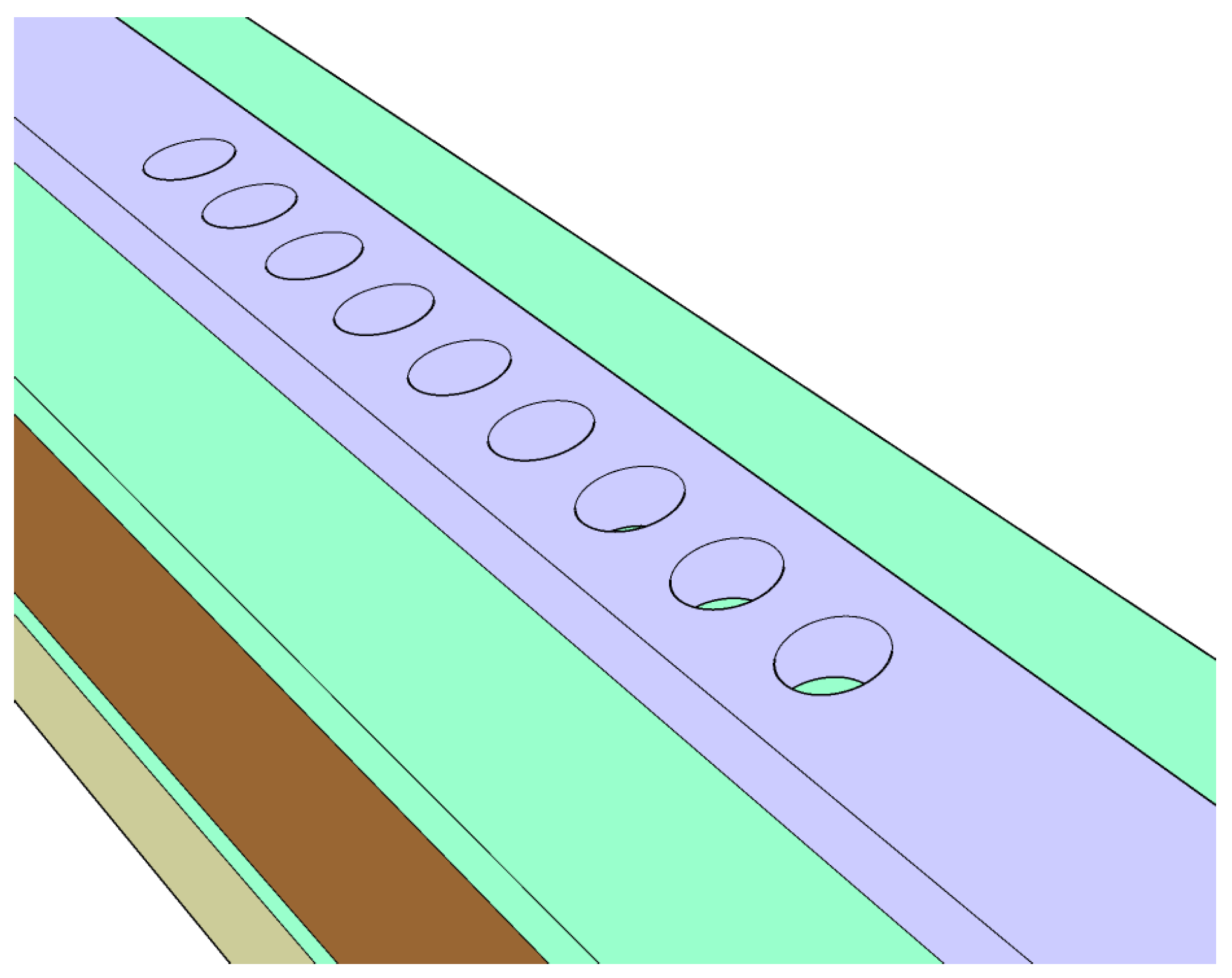
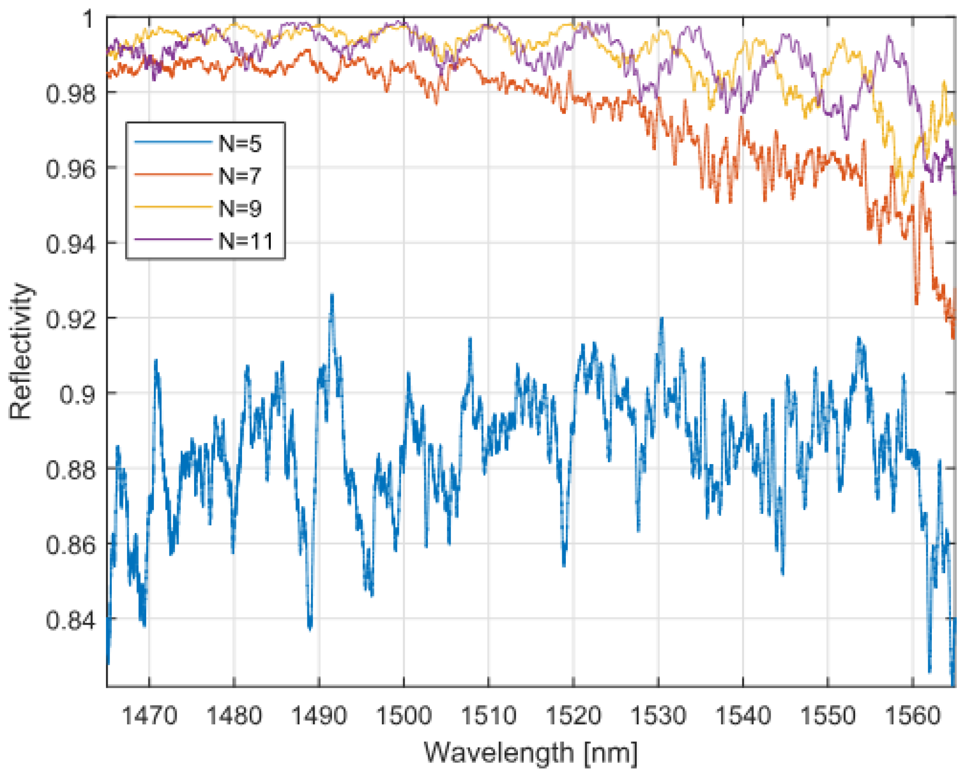
2.1.1. Light Reflection

Shallow-etched distributed Bragg reflectors (DBRs) are generally used as broadband reflectors on the IMOS platform. Alternatively, photonic crystal (PhC) reflectors have been designed and are introduced, providing an ultra-short, high-reflectivity device that is seamlessly integrated due to its simple design. The reported reflectors feature a large variety of bandwidths and reflectivity coefficients, which is essential for building lasers. For robustness, the PhC reflectors are etched in a 700 nm-wide waveguide instead of the standard 400 nm-wide waveguides. A schematic of the PhC reflector is shown in Figure 2.
The reflectivity of the reflectors is experimentally validated. Two methods have been used to characterize the structures: a Fabry–Pérot method and a direct four-port characterization method. The methodology is extensively covered in [16]; only the final results are shown here. The measured reflectivity at the peak value is shown in Table 1, the devices cover the c- and s-band with less than 0.5 dB reduction in reflectivity. It is observed that the direct method yields better results, especially for higher reflectivity.
The insertion loss of these reflectors is an important parameter; however, it could not be accurately measured with the available characterization structures.
The PhC reflectors demonstrate above 99% reflectivity for nine holes; higher is possible by further increasing the number of holes. The reflector with nine holes is only 3.1 µm long, excluding the taper. The reflectivity and bandwidth of the reflector are shown in Figure 3.

2.1.2. Polarization Control

Besides the amplitude and the phase of optical signals, the polarization state can be exploited. On-chip polarization handling is essential for a state-of-the-art photonic integration platform, and it enables new features, e.g., sensing and optical communication formats. A polarization converter (PC) is the key component for enabling polarization handling. PCs on the InP membrane platform were first introduced in 2012 [17]. This device is based on mode hybridization, and the most recent design [18] is ultra-short: less than 5 µm long. In comparison, converters based on directional couplers are typically at least an order of magnitude longer. A schematic of the PC is shown in Figure 4.
With this device, a polarization rotation device is added to the platform, and in a Mach–Zehnder interferometer structure, a polarization splitter circuit can be realized. The performance parameters of the reported PCs demonstrate a polarization conversion efficiency (PCE) of more than 99% and a simulated insertion loss of less than 0.6 dB. Experimentally, aPE as high as 97% was achieved. The PC has recently been fully integrated in the twin-guide active–passive platform [19], adding this functionality to the active–passive platform, by reusing the n-doped InP layer for the top of the triangular sections. Hereby, no changes to the epitaxial stack are required for this component.

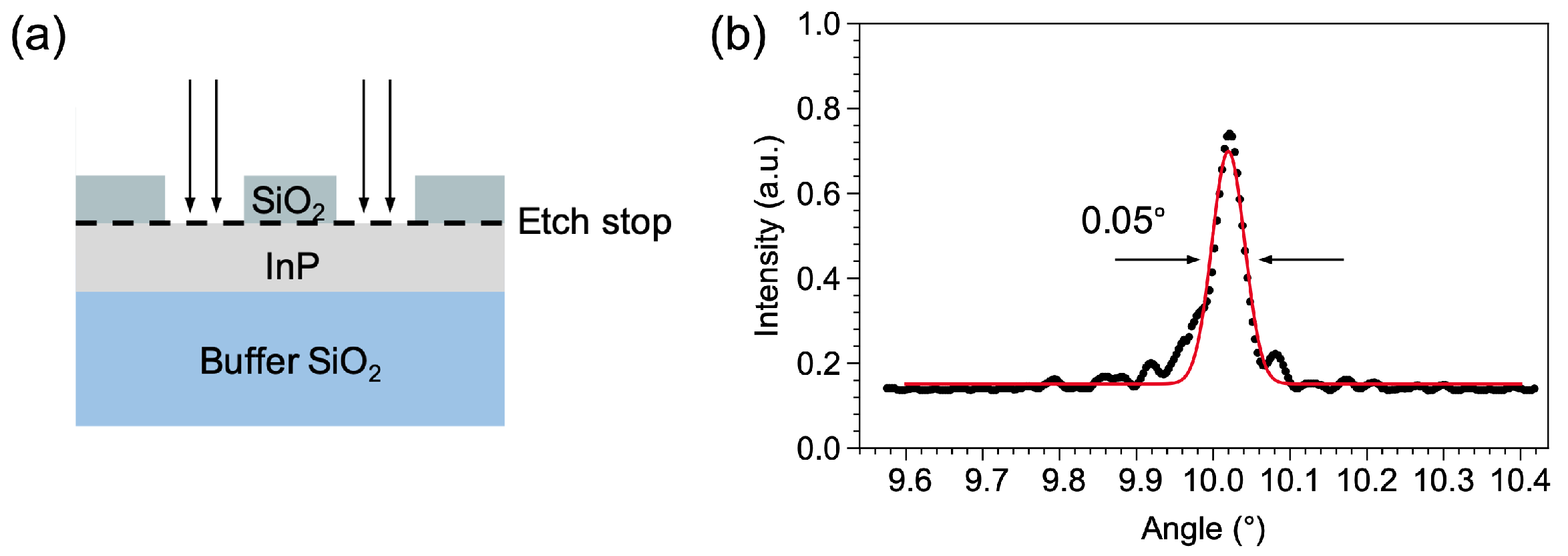
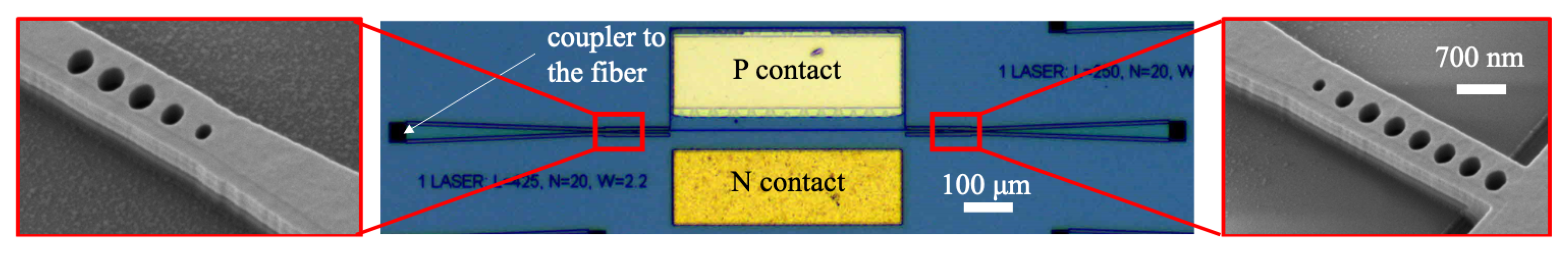
2.1.3. Free-Space Interfacing

Optical antenna bridges are in-plane integrated photonics with free space. One major application area for such functions is automobile light-based detection and ranging (LiDAR), which requires pencil-like beam emission with a high angular resolution [20]. The key challenge here is the accurate control of light scattering to create a diffraction-limited aperture. For shallow-etched grating antennas, normally a very small etch depth—in the order of single nanometers—is required, bringing in process control complexities [21]. Here, this issue is addressed by using SiO2 gratings on top of the InP waveguide, as seen in Figure 5a. In this design, an etch-stop at the SiO2/InP interface is obtained, since the fluorine-based etching recipe for SiO2 has a strong selectivity over InP (30:1). In 2019, optical antennas based on this design with millimeter-scale emission apertures were demonstrated on the IMOS platform [22,23]. A metal mirror is additionally integrated, leveraging the double-sided processing technique, to boost the upward emission efficiency.
For a 2 mm-long antenna, far-field measurement shows a 0.05° full-width half maximum (FWHM) beam width, as seen in Figure 5b. This is approaching the diffraction limit. The emitted beam is steered by wavelength tuning, achieving a steering range of 13° and over 250 total resolvable points. This is limited by the input tunable laser, and the grating antenna presented here is inherently broadband [23]. In 2023, the integration of this grating antenna with active components into a single process flow is further demonstrated [24,25], showcasing the potential for full system-level realization on the IMOS platform.

2.2. Active Building Blocks

The InP material system for PICs provides a compelling solution for realizing active components that can be seamlessly integrated with passives. Here, we review the recent development on how each active function is implemented on the InP membrane platform.

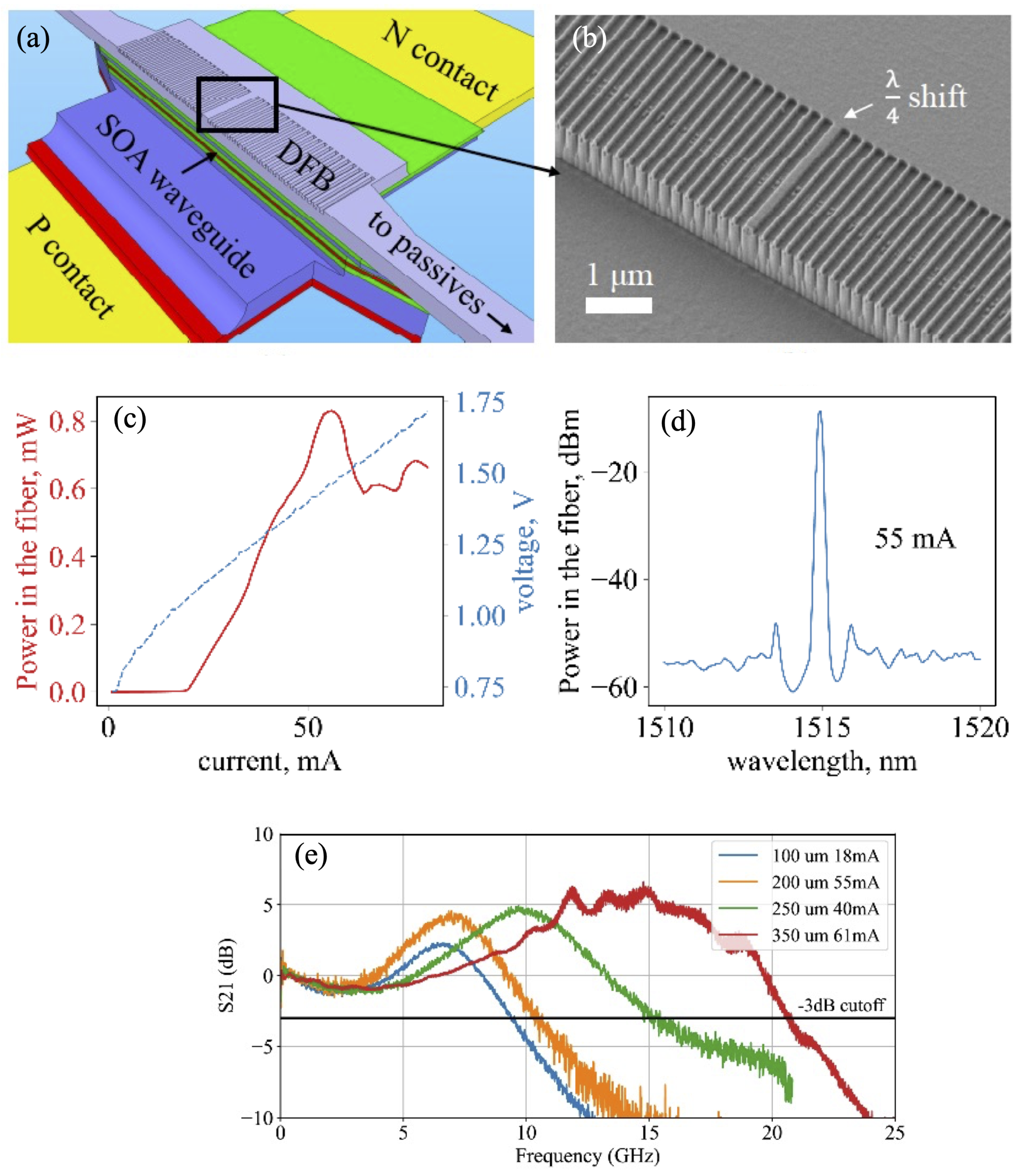
2.2.1. Light Generation

The O- and C-bands are widely employed wavelengths for today’s PIC applications [26], and they coincide with the optical fiber communication standards. InP, together with the ternaries and quaternaries in the material system, offers efficient light generation with high wavelength tunability in these bands. There is a long research history on conventional InP-based semiconductor optical amplifiers (SOAs) and lasers [2]; however, it was not until recent years that those functions were miniaturized and realized on a membrane platform [27,28].
The IMOS platform utilizes flexible epitaxy techniques to achieve active–passive integration or active-modulator integration. For modulators, the number of quantum wells can be as high as 25. The SOA epi-structure is a vertical p-i-n diode, grown on top of the intrinsic InP waveguiding layer. The active waveguide is then fabricated in a double-sided etching process, in which the sidewalls of the SOA are etched from different sides of the membrane. A cross-sectional schematic of the final fabricated SOA is shown in Figure 6a. At the outputs of the SOA, the lasing mode is vertically coupled into the fundamental mode of the passive InP waveguide, which is positioned above the SOA layers after bonding. Low-reflection coupling is ensured by using 2-stage tapers, as seen in Figure 6b. This SOA structure is called a twin-guide [29], and it enables seamless integration of SOAs into complex laser cavities, as well as into more sophisticated photonic circuits. By carefully tuning the taper structure, the TE and TM modes can be simultaneously coupled. This is explored in [30], where O-band SOAs with a polarization dependence of less than 1 dB are realized.
To further improve the flexibility and reduce the overhead in active–passive coupling, a butt-joint interface has been developed recently [31]. In this case, the active waveguide is directly connected to the passive InGaAsP waveguide, while the claddings are tapered for reflection suppression, as seen in Figure 6c. Through this design, the coupling length has been reduced from 50 µm to 25 µm, allowing for the realization of more compact lasers and larger-scale active–passive integration. Distributed feedback (DFB) lasers can be realized on IMOS utilizing the native SOA. Figure 7a shows a schematic image of such a DFB laser realized with the twin-guide scheme. The DFB gratings are shallowly etched into the passive InP waveguide, as seen in the SEM image in Figure 7b. Figure 7c shows the LIV curves of a 400 µm-long DFB laser with a λ /4 shift in the center. Output optical power levels of up to 1 mW in the fiber are demonstrated. Considering the 3–5 dB coupling loss, the facet power is in the order of 2–3 mW. The threshold current is around 20 mA. A high side-mode suppression ratio of over 45 dB is also obtained, as seen in Figure 7d. Kinks observed in the LI curve may be attributed to mode hopping due to reflections from grating couplers, taper tips, or due to a change in the refractive index inside the cavity because of heating and carrier injection. The shortest DFB lasers operating in continuous-wave (CW) have an active region length of 100 µm [31] and a threshold current as low as 6 mA. Direct modulation experiments have been performed, as seen in Figure 7e. The short 100 µm-long DFB laser shows a bandwidth up to 21 GHz [31], making them useful for optical communications. Tunable photon–photon resonance (PPR) is achieved by integrating on-chip phase shifters with the DFB lasers [32]. These devices showed a tuning of the PPR frequency of 5 GHz, significantly relieving the stringent phase-matching requirement for high-speed operation. These lasers were used for back-to-back data transmission experiments of non-return-to-zero (NRZ) signals, demonstrating a data rate of 28 Gbit/s.
Apart from DFB lasers, a variety of lasers can also be realized by combining the native SOA with passive circuits on the same membrane. Multi-mode lasers with strong DBR gratings and photonic crystal reflectors (PhC) were demonstrated (Figure 8). Reflectivity up to 99% with a device around 10 µm long is demonstrated [16]. The availability of different reflectors and cavity types along with design flexibility makes the IMOS platform promising for laser integration and complex laser designs, which will be further demonstrated in Section 4.

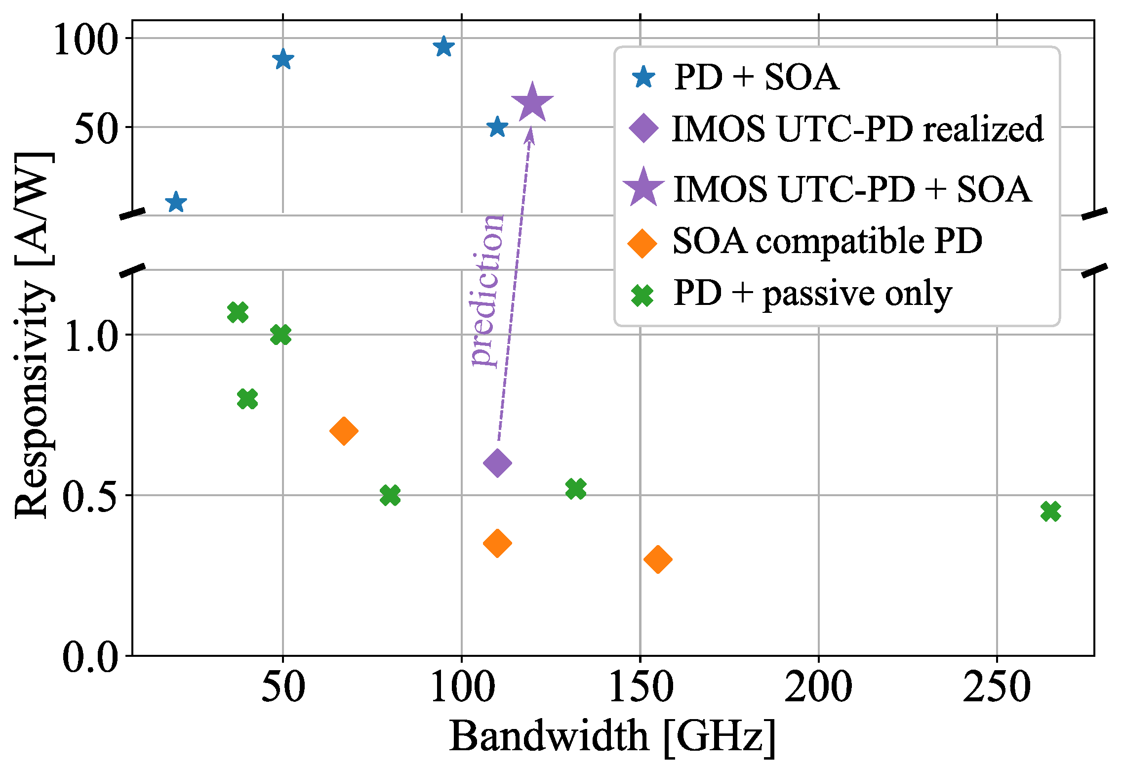
2.2.2. Light Detection

Uni-traveling carrier photodiodes (UTC-PDs) have been developed on the IMOS platform for ultra-high-speed light detection. Not only is this an important building block for optical communications, it can also enable applications in microsecond and terahertz technologies [34].
We have realized a state-of-the-art UTC-PD that is compatible with SOAs and passives within the same process flow. The IMOS UTC-PD uses the 300 nm InP waveguide layer as an electron drift layer, which is sandwiched between a p-doped InGaAs absorber and an n-doped InP collection layer. The p-InGaAs absorber, located below the waveguide, consists of a graded p-doping section and an undoped region, which together also serve as a p-contact. The n-InP collection layer on top of the waveguide is 80 nm thick and functions as the n-contact of the device. The standard 300 nm passive IMOS waveguide layer is sufficiently thin to enable transit time bandwidths of approximately 96 GHz at electron saturation velocity. A schematic of the UTC-PD can be seen in Figure 9a.
The doping profile of the absorber creates an intrinsic electric field that boosts electrons to an overshoot velocity of 3 × 107 cm/s [35], potentially increasing transit time bandwidths up to 148 GHz. Combined with a miniaturized absorption volume that results in high RC bandwidths, bandwidths beyond 110 GHz have been measured, as shown in Figure 9b [36]. The curves demonstrate a clear bias dependence, attributed to the lack of band-smoothing layers. Including these layers has proven to result in high performance even at zero bias [37]. The direct waveguide integration results in the immediate coupling of the optical field into the absorption region. Combined with high mode confinement, this enables devices as small as 10 µm2 while still achieving a responsivity of 0.6 A/W. The butt-joint design of the IMOS UTC-PD, combined with the flexible two-sided processing scheme, results in inherent compatibility with other photonic and electric building blocks. Figure 9c shows a UTC-PD integrated with an optical waveguide, a grating coupler, and an RF choke. Furthermore, by flipping the UTC-PD epilayers, a single-growth epitaxial layer stack can be realized, hosting UTC-PDs, SOAs, and high-efficiency thermo-optic phase shifters. All three devices share the same InP n-contact and undoped InP waveguide layer, without requiring design alterations to the SOA, phase shifter, and passive building blocks. This results in a single, unified process flow without the need for regrowth, reducing fabrication complexity. Molecular beam epitaxy, using beryllium as the p-dopant, is employed to avoid dopant diffusion during growth, a common issue with zinc dopants in MOCVD. The combination of these building blocks enables novel integrated systems, such as fully integrated CW-THz spectrometers, and allows for complex optical transceiver designs, including on-chip optical amplification or on-chip antennas.
Figure 10 shows a comparison of the IMOS UTC-PD with the state-of-the-art high-performance photodiodes (PDs) integrated into photonic integrated platforms. These include Si-Ge-based PDs integrated on passive silicon-on-insulator platforms [38,39,40,41] and III-V-based PDs on passive-only InP platforms [42,43]. Additionally, detectors on SOA-compatible III-V platforms, such as the IMOS platform [35,36,44], and transfer-printed UTC-PDs on a SiNx platform [37], have been demonstrated. Furthermore, the combination of SOAs and high-speed PDs on a single platform has been shown to allow for responsivities beyond the passive fundamental limit due to signal amplification by the SOA [45,46,47,48]. The realized UTC-PD integrated on IMOS proves to be competitive in terms of bandwidth-responsivity performance, particularly compared to other SOA-compatible implementations. The integration with SOAs can enhance responsivity values by a factor of 10, assuming an optical gain of 10 dB, as demonstrated with the dual-pass SOA structure [49]. Combined with an estimated maximum bandwidth of around 120 GHz [36], the predicted performance of the IMOS UTC-PD + SOA is also shown in Figure 10 and is expected to be competitive with other high-speed PD + SOA platforms.

2.2.3. Phase Control

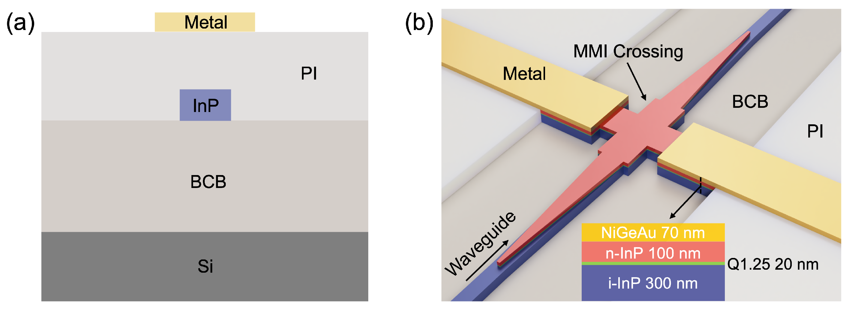
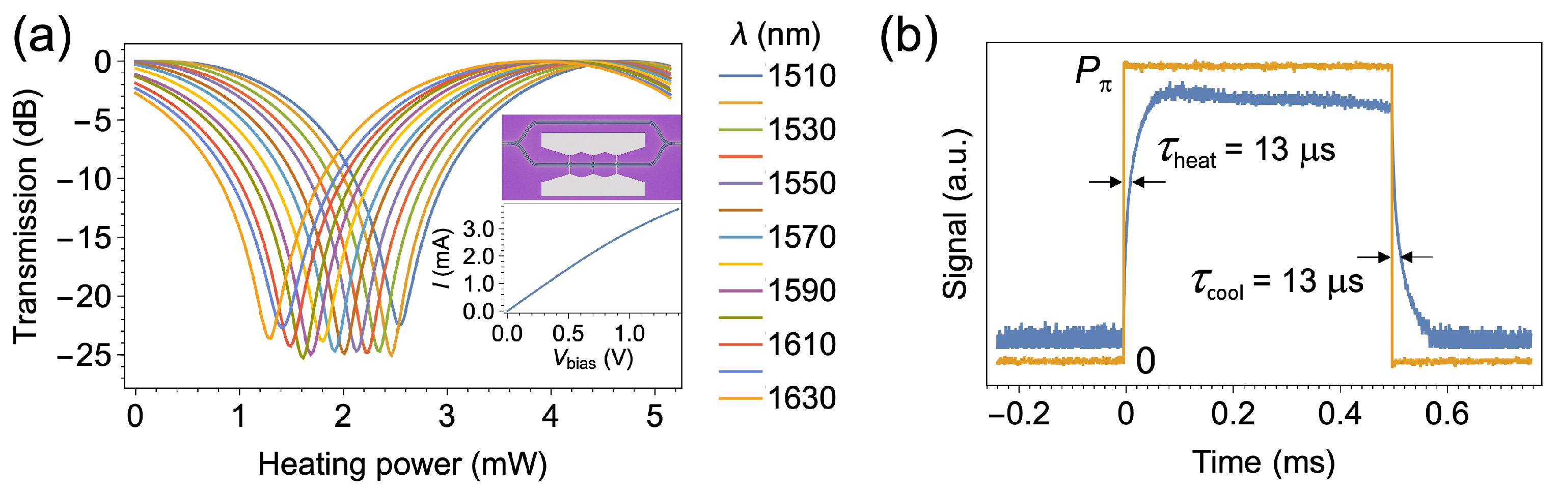
Low-Energy Thermo-Optic Tuning
Phase control is essential for any photonic platform to realize active tuning functionalities. Integrated phase tuning on the IMOS platform is available via the thermo-optic (TO) effect, which is reliable when telecom-grade modulation speed is not required. Fast electro-optic (EO) phase modulation on IMOS can be realized using EO polymers that will be introduced later in Section 2 and Section 3. Two types of TO phase shifters (TOPSs) are available on the IMOS platform: a conventional metal-strip-based design [50] and an ultra-compact and efficient microheater exploiting direct heating of the waveguide [51]. Both designs are directly compatible with the platform and can be unified under the same process flow. The cross-sections of both designs are shown in Figure 11a and Figure 11b, respectively. The cross-section of the metal-strip-based design shown in Figure 11a is similar to what is commonly used on the silicon-on-insulator (SOI) platform [52,53]. In this design, the heat generated in the metal strip needs to go through the µm-thick top cladding, i.e., the polyimide (PI) planarization layer, before reaching the optical waveguide. This imposes challenges on the power efficiency, tuning speed, and footprint.
Such issues can be tackled by directly heating the waveguide using an epitaxially-grown n-doped layer on top of the i-InP waveguiding layer [51], as seen in Figure 11b. The same n-InP layer is shared with the n-contact for PCs and SOAs, and therefore they can be seamlessly integrated, allowing for high versatility in circuit design. To reduce the optical absorption from the close placement of accessing metal tracks to the optical mode, a 1 × 1 multimode interference (MMI) crossing is used, so the optical path and electrical conduction do not interfere with each other. This design offers physically minimized heat capacity and therefore a high-power efficiency of 2.2 mW/ π for the wavelength of 1550 nm and a small thermal time constant of 13 µs, as seen in Figure 12a and Figure 12b, respectively. The dimension of the n-InP conduction layer has been carefully designed to allow for low-voltage (1–2 V) driving, compatible with CMOS electronics. Since heat is centralized in the MMI crossing compared to the metal-strip-based design, thermal crosstalk is also reduced. At a 13 µm pitch, we measure 3.6% power leakage to the nearby channel. This low amount of thermal crosstalk offers high versatility in circuit design, as the design rules can be much more relaxed. For example, this thermal crosstalk level has a negligible impact on the performance of optical switches [54] or optical phased arrays [55].
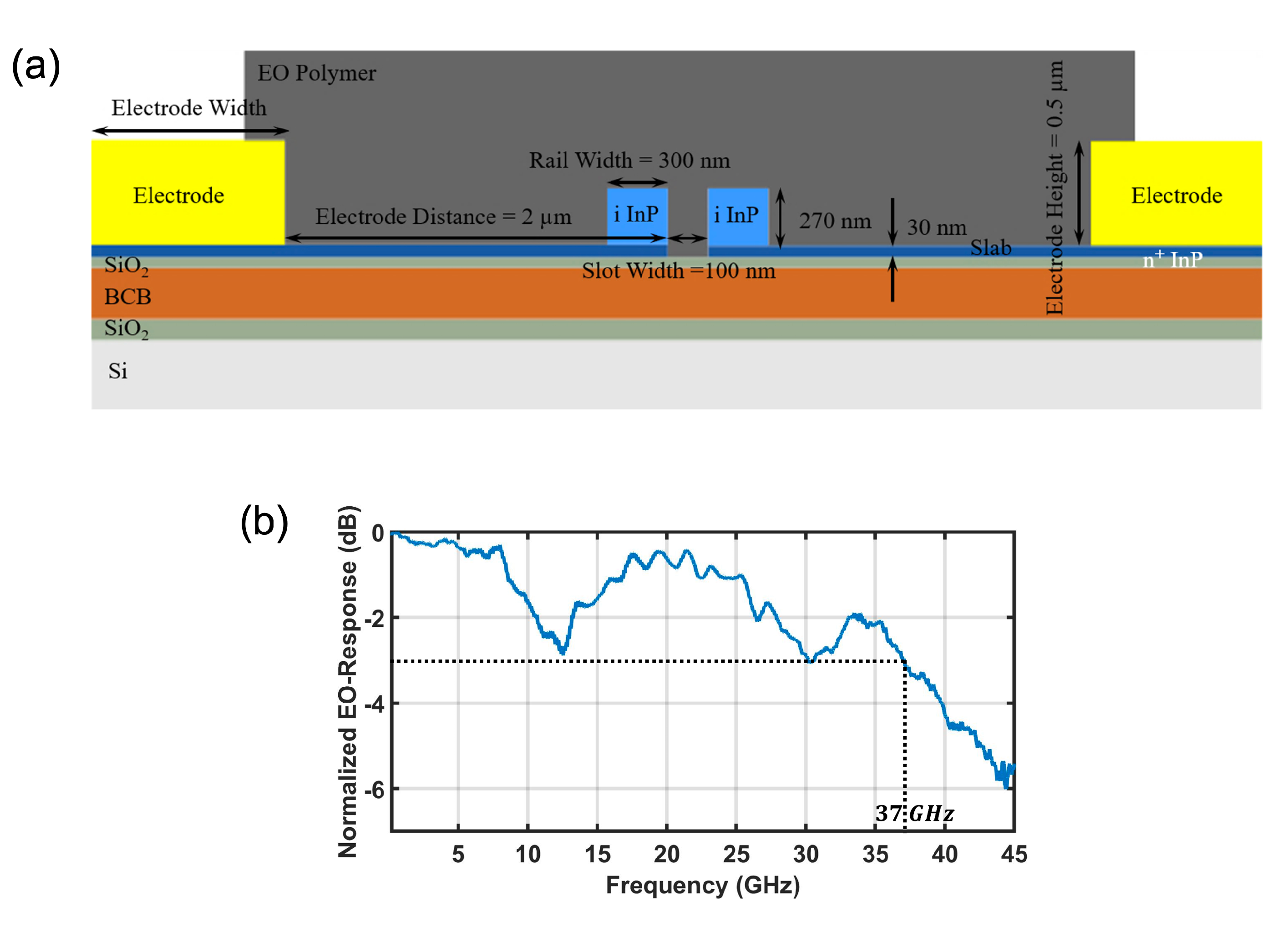
High-Speed Modulation
The IMOS platform also opens opportunities for novel phase modulators with reduced footprints. Compared to substrate-based platforms, optical modes on the membrane platform are more accessible for manipulation, due to the simple strip waveguide cross-section, allowing for the realization of slot and plasmonic waveguides. These could offer optical confinement enhancement and potentially stronger light–matter interaction. In 2020, an InP slot-waveguide-based phase modulator on the IMOS platform was first demonstrated [56]. Organic electro-optic (OEO) polymer filling the slot waveguide is leveraged to achieve field-induced refractive index change. The device cross-section with design parameters is shown in Figure 13a. With a 100 nm-wide slot, the calculated optical confinement in the OEO polymer approaches 30%. With a propagation loss of 150 dB/cm in the slot waveguide section, the loss of the 500 µm-long slot waveguide modulator is around 7.5 dB. Here, a polymer mainly optimized for thermal stability is used, whose bulk r33 strength (a measure of the electro-optic activity) is 110 pm/V [57]. In the first attempt, a modulation efficiency, as quantified by the half-wave-voltage-length product VπL of 3.9 Vmm is measured. The VπL can be further reduced to 1 Vmm levels if high-efficiency polymers are utilized [58]. The 3 dB electro-optic modulation bandwidth is characterized to be 37 GHz, as plotted in Figure 13b. This performance is comparable to the state-of-the-art realizations with Si slot waveguides [59]. With further geometric and doping optimizations, a beyond 100 GHz bandwidth is predicted [60].
Plasmonic-organic-hybrid (POH) modulators could potentially allow for smaller devices and potentially higher bandwidth [61,62]. This is through further confinement enhancement with a plasmonic slot waveguide and smaller RC time reduction from the high-conductivity metals as compared to doped semiconductors. The same OEO polymer can be used in the metal slot waveguide to introduce index change. A 10 µm-long POH modulator was recently realized on the IMOS platform [57]. With a gold slot waveguide of 200 nm slot width and 300 nm metal thickness, a calculated 72% optical confinement is obtained. The optical loss of the plasmonic modulator is around 5 dB. In the experiment, we measured a VπL of 0.44 Vmm, an almost 10-fold improvement compared to the InP slot waveguide modulator with the same OEO polymer. This is a combined result of the higher confinement and effective index of the plasmonic mode. Preliminary high-speed characterization showed a 3 dB bandwidth of more than 25 GHz, and this is currently limited by the measurement technique [57].

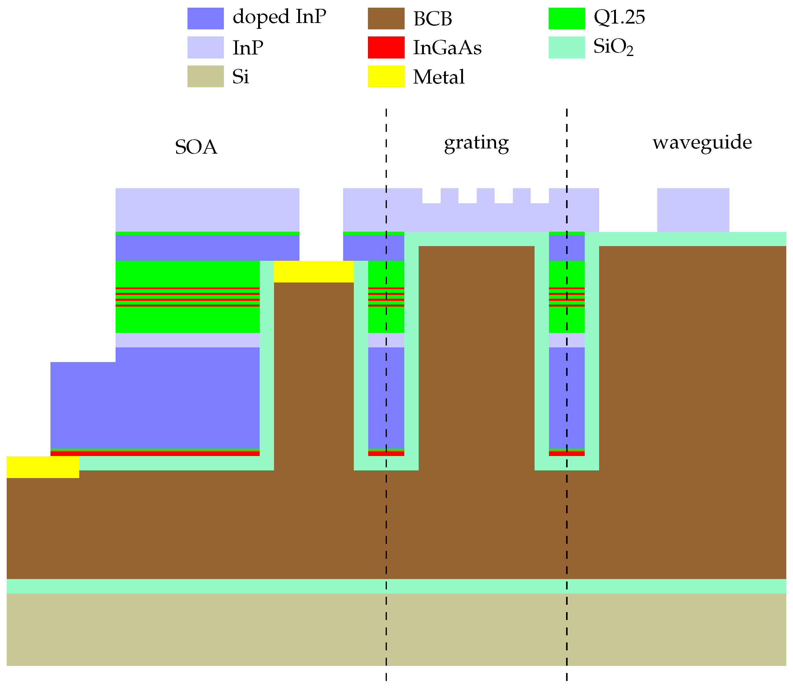
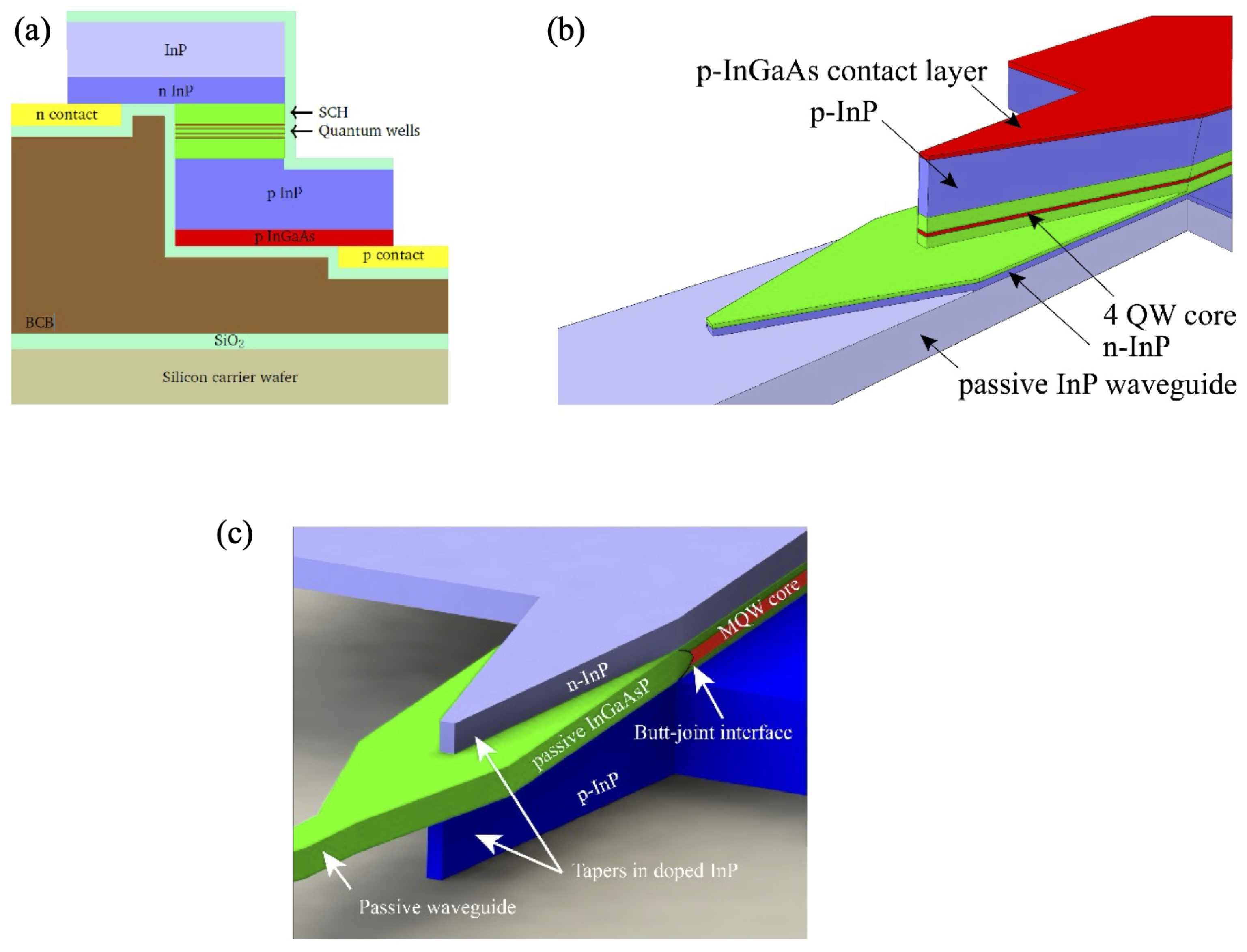
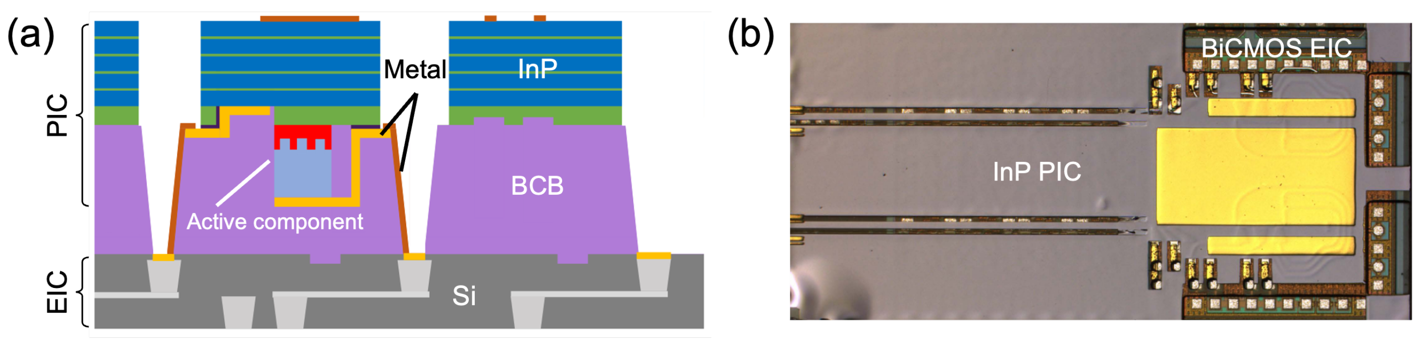
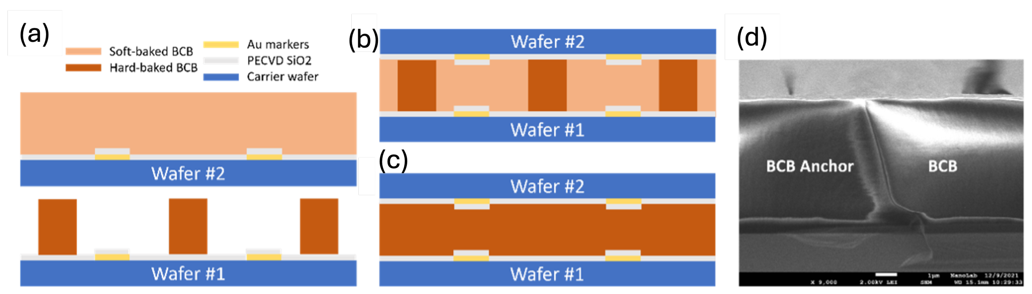
3. Membrane Integration Technology

The IMOS technology provides a single active–passive photonic layer that can be versatilely transferred to different substrates, while all photonic components are integrated in a continuous InP membrane. This is in contrast to the conventional die or wafer bonding approach used in InP-Si heterogeneous integration, where only the active functions are realized in InP, and passives are fabricated in Si [63,64]. The unique advantage of the IMOS approach is the decoupling of the complete photonic circuitry from the substrate, allowing for versatile wafer-scale assembly with various technologies. Furthermore, integrating all functions in InP also enables advanced active–passive integration schemes such as butt-joint regrowth [65].
Recently, the co-integration of a monolithic InP photonic layer with SiGe BiCMOS electronics has been realized via this approach [66]. Compared to conventional wire-bonding-based electronic packaging, the link length is reduced from centimeters to micrometers, and the interconnect footprint can be shrunk by more than one order of magnitude. Figure 14a shows the cross-sectional structure of such an E-O integration concept. A thick BCB bonding layer is applied here to tolerate up to 9 µm surface topology variations on the electronics wafer. To reduce the performance degradation in the electronic integrated circuit (EIC) due to postprocessing, low-temperature (240 °C) bonding is performed. A 4 µm pre-bond wafer-to-wafer alignment accuracy is achieved via an optical alignment process. However, the post-bonding wafer-to-wafer shift was 89 µm due to residual strain release during the bonding process [67,68]. The through-polymer vias (TPVs) are fabricated using a reflow-and-etch process to realize sloped sidewalls [51,66]. Finally, the metal interconnection is fabricated with evaporation and electroplating. Figure 14b shows the final fabricated dual-channel transmitter which contains two InP-based externally modulated lasers (EML) integrated with their BiCMOS drivers [66,69]. Characterization of the transmission lines confirmed RF links with 3 dB bandwidth exceeding 67 GHz between the PIC and EIC, validating the integration concept.
To improve the alignment accuracy for wafer-to-wafer integration, a novel process with BCB ‘anchors’ was developed in 2023. This process is illustrated in Figure 15a–c. Firstly, BCB anchors are patterned and hard-baked on the source wafer, while the target wafer is coated with soft-baked BCB allowing for it to reflow. Then, the two wafers are brought together under a vacuum. In this step, the hard-baked anchors penetrate through the liquid BCB layer and reach the target wafer, providing a solid backbone locking the two wafers in place and improving thickness uniformity. Finally, the entire stack is hard baked for full BCB crosslinking. A void-free and uniform interface between the BCB anchors and bonding layer BCB is achieved, as shown in Figure 15d [70]. With this technique, the post-bonding alignment accuracy is improved by one order of magnitude, entering the below-10 µm regime. The thickness uniformity of the bonding layer is increased by a factor of 2–3 even with thick BCB layers in the range of 8–16 µm. The additional alignment error attributed to membrane stretching due to the mismatch of thermal expansion coefficients of the wafers is further understood and quantified with e-beam lithography [71]. The conclusion is that these distortions can be predicted and pre-compensated to achieve even higher post-bonding accuracy. Combining BCB anchors and membrane stretching compensation, high topology tolerance, uniformity, and alignment accuracy can be simultaneously achieved, potentially allowing for the realization of ultra-dense micro-vias [72] for large-scale photonic–electronic integration.
The thick BCB layer provides good thermal insulation between different building blocks. Heat dissipation can be realized where needed, using thermal shunts to the substrates [30]. In the demonstration conducted in 2023, a 4 µm-thick electroplated gold is used as the heat conduction material to the substrate, which acts as the heatsink. This approach effectively decreases the SOA core temperature by at least 23 °C. This heat-sinking scheme is also compatible with state-of-the-art packaging solutions [73].

4. Integrated Sub-Circuits

A wide range of circuits is enabled by our generic technology. Highlights are discussed in this chapter.

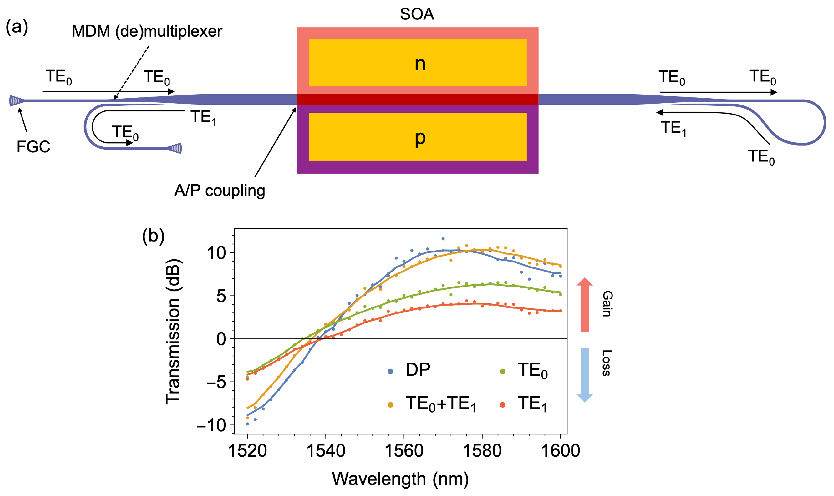
4.1. Mode-Division Multiplexed Circuits for Efficiency Boost

Mode-division multiplexing (MDM) is an effort to explore light’s additional degree of freedom—the mode space—and it has been demonstrated in passive circuits [74,75] and modulators [76,77,78]. In modulators, the light–matter interaction can be enhanced several times by MDM, which reuses the same functional section multiple times, resulting in many-fold efficiency enhancement [78]. In 2023, for the first time, this concept was applied to SOAs, one of the most power-hungry components in PICs [49]. In Ref. [49], a resonance-free double-pass (DP) SOA is reported with the active–passive IMOS technology, whose circuit schematic is shown in Figure 16a. In this DP-SOA, the gain section is a bus waveguide supporting both the T E 0 and T E 1 mode, while optical interfacing with fibers is realized with the fundamental mode. Starting from the input grating coupler, the light first travels through the gain section in the T E 0 mode, is converted into the T E 1 mode, is then multiplexed into the bus gain section and amplified again, and finally is demultiplexed/converted back into the T E 0 mode. Therefore, the optical gain becomes the total gain in two passes minus the excess loss from the (de)multiplexers and active–passive coupling. The measured optical gain for both the DP case and standalone T E 0 and T E 1 gain are plotted in Figure 16b for comparison. As can be seen, the DP gain matches well with the total gain of T E 0 and T E 1 , confirming the multiplexed gain section. As a result, a maximum 87% gain enhancement and 300% wall-plug efficiency (WPE) enhancement are obtained without needing more electrical input power. The highest WPE achieved is over 10% for a 5 dBm on-chip optical input power.

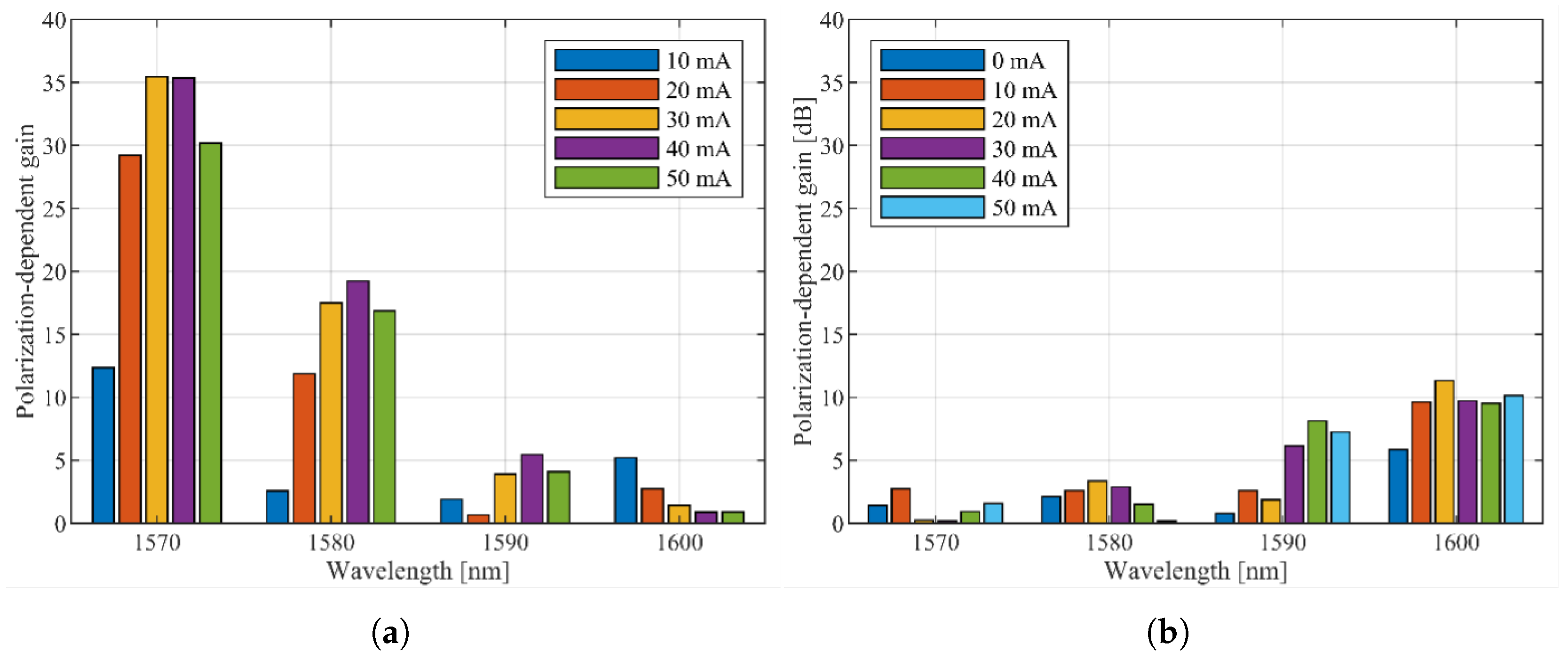
4.2. Polarization-Independent Quantum Well SOA

An application can require equal gain for TE and TM modes from a semiconductor optical amplifier (SOA). On most platforms, the layer stack is optimized to provide optimal gain for the TE mode, hence the TM mode experiences significantly lower gain. A common figure to indicate the difference between gain for TE and TM modes is the polarization-dependent gain (PDG). To minimize the PDG, several well-known methods are available, e.g., epitaxial engineering of the gain medium [79,80] or placing a polarization rotator between two half-length SOAs [81,82]. Changing the active core has a high impact on the photonic platform, whereas the integration of a polarization rotator typically has a lower impact. However, using bulk material instead of QWs does not require a polarization rotator. Depending on the application, this can be preferred over the QW core with polarization rotator.
A polarization-independent SOA was demonstrated for the first time in [19] using the concept described above—placing a polarization rotator between two half-length SOAs, as shown schematically in Figure 17. The polarization rotator described in Section 2 is used in this circuit. The resulting PDG has been measured for wavelengths in the range of 1570–1600 nm, as shown in Figure 18.
The PDG is improved significantly from up to 35 dB for a standard SOA to below 3 dB for the full range of injection currents at 1570 nm and 1580 nm.

4.3. Dual-Polarization Light Source

An integrated light source that can provide both TE and TM light simultaneously can be useful for communication and sensing applications. Various methods can be used to achieve this, e.g., epitaxial engineering to achieve equal gain for TE and TM [80,83,84] or rotating the polarization outside of the laser cavity. On the InP membrane platform, such a light source has been demonstrated utilizing a Fabry–Pérot laser and a polarization converter (PC) [85]. With this combination, a light source generating both TE and TM polarizations is created by rotating the output on one side of the laser with a PC. The schematic of this light source is shown in Figure 19, and a SEM image is shown in Figure 20. The output of both polarizations is measured on both sides.
Although the optical power measured from this light source is low at around −20 dBm, the power balance between the two modes is promising, with less than a 2 dB difference in power, measured in the fiber for each of the outputs. These values are not compensated for any excess loss in the couplers or waveguides and can be further improved by lowering the active–passive taper loss.

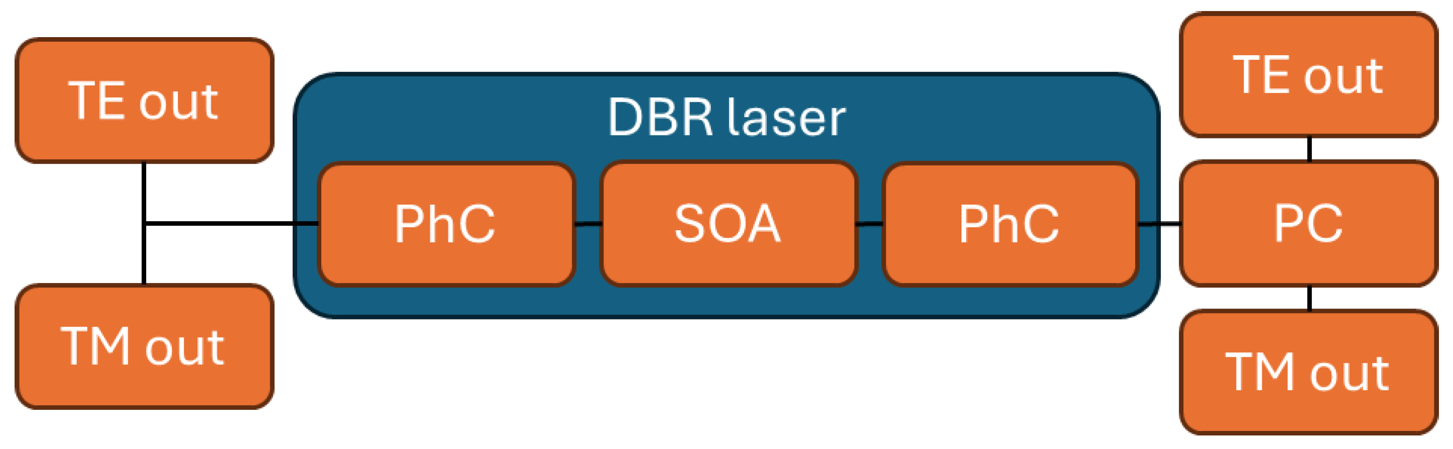
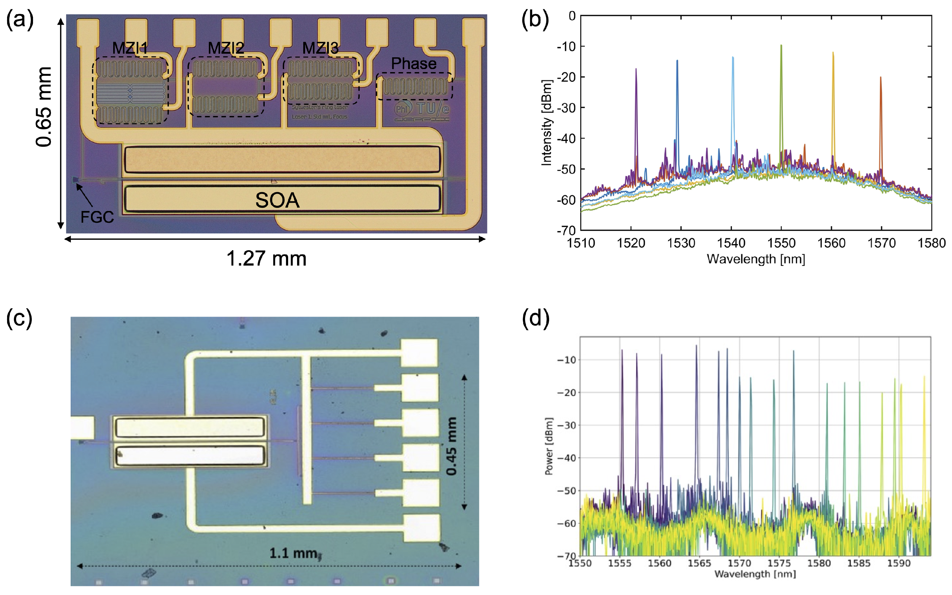
4.4. Compact Tunable Laser

The seamless integration of active and passive components in the same nanophotonic InP membrane enables complex active–passive circuits with miniaturized footprints. In 2023, a widely tunable laser was realized on the IMOS platform under a footprint of 0.83 mm2 [25], four times smaller than a similar circuit realized on a substrate-based platform [86]. This footprint is further reduced by optimizing the cavity design and mode selection mechanism [87], resulting in a footprint of only 0.495 mm2. Microscope images of the fabricated tunable lasers are shown in Figure 21a,c. Laser (a) comprises three tunable MZIs, one phase tuning section, and an SOA. Each stage of the cascaded MZIs has a different arm length difference. All the components are connected to form a ring structure. Wavelength selection in the ring is achieved by aligning the peak transmission of each MZI and fine-tuning the phase section. In the experiment, a 50 nm tuning range is achieved, as seen in Figure 21b. This is currently limited by the gain spectrum, while the tuning mechanism itself supports a range of over 100 nm [88]. The peak output power collected in a single-mode fiber is −10 dBm. When offsetting the fiber grating coupler (FGC) coupling loss, this means 0 dBm on-chip output power. Similarly, laser (b) integrates an SOA gain section and a parallel MZI wavelength selection section. The parallel configuration allows for further footprint reduction. As seen in Figure 21c, the parallel MZI is made of four arms each connected to a reflector. The wavelength is selected when the reflected waves from all four arms are in phase, as determined by the thermos-optic phase shifter on each arm. A 40 nm tuning range is demonstrated with this design, but this is limited by the gain spectrum. The demonstration of such compact widely tunable lasers could contribute to the further realization of complex PIC-based systems such as integrated optical beam steerers or optical coherence tomography (OCT) light sources.

5. Novel Material Integration

In this section we discuss newly enabled functionality by integrating novel materials on the IMOS platform. The materials are phase-change materials, MOKE materials, and metal garnets.

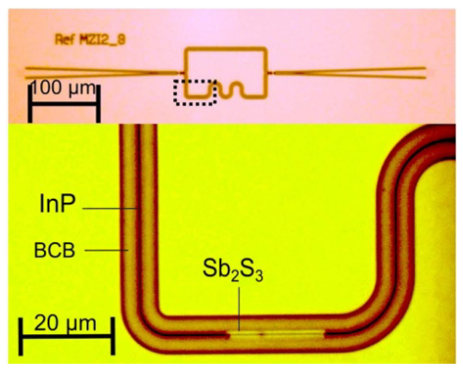
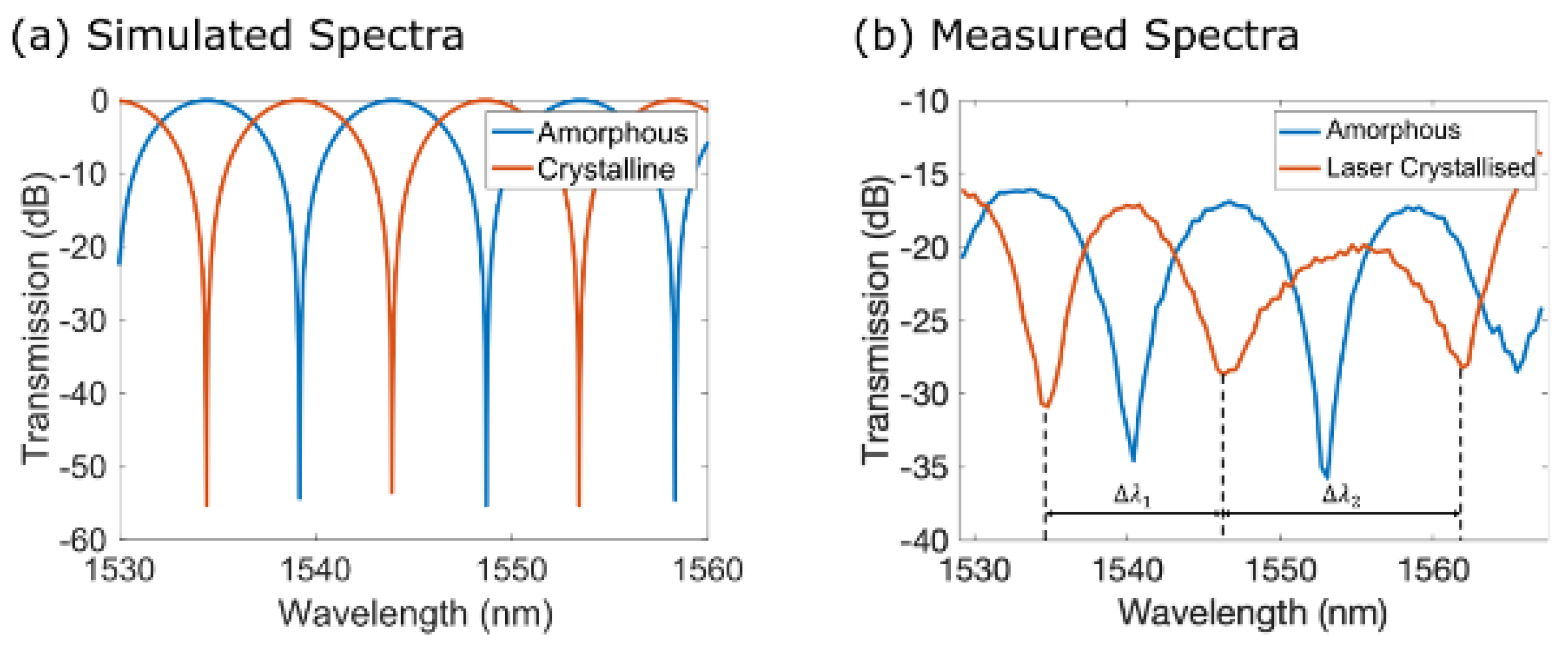
5.1. Phase Change Material: Sb2S3

Phase change materials are a promising addition to PICs since they open the way for reprogrammable optical chips [89]. The optical devices this integration yields can serve a similar role as programmable gate arrays in electronics, enabling complex logic circuits and neural networks fully integrated on a chip [90]. Such devices have been demonstrated, with applications in optical networks [91] and neural networks [92]. Sb2S3 has the largest band gap among all phase change materials currently being explored for programming photonic components [93]. The material is transparent for near-infrared wavelengths, can be switched thousands of times, and multiple optical states can be achieved by partial amorphization or growth crystallization tuning [93,94]. A Sb2S3-tuned Mach–Zehnder interferometer (MZI) is demonstrated on an InP membrane [95]. Optical switching behavior is realized by switching between amorphous and crystalline states of the Sb2S3, which have refractive indices of 2.85 and 3.20 for a wavelength of 1550 nm, respectively. By placing the material directly on top of a membrane waveguide, the propagation constant of the mode can be changed. A microscope image of the device is shown in Figure 22, and the performance of the device is shown in Figure 23.
Laser crystallization of the Sb2S3 resulted in 18 dB attenuation at a wavelength of 1540 nm. Re-amorphization was not possible due to thermal damaged to the BCB layer. This can, in the future, be prevented by adding a thermal barrier layer, e.g., MoS2, between the Sb2S3 layer and the InP waveguide.

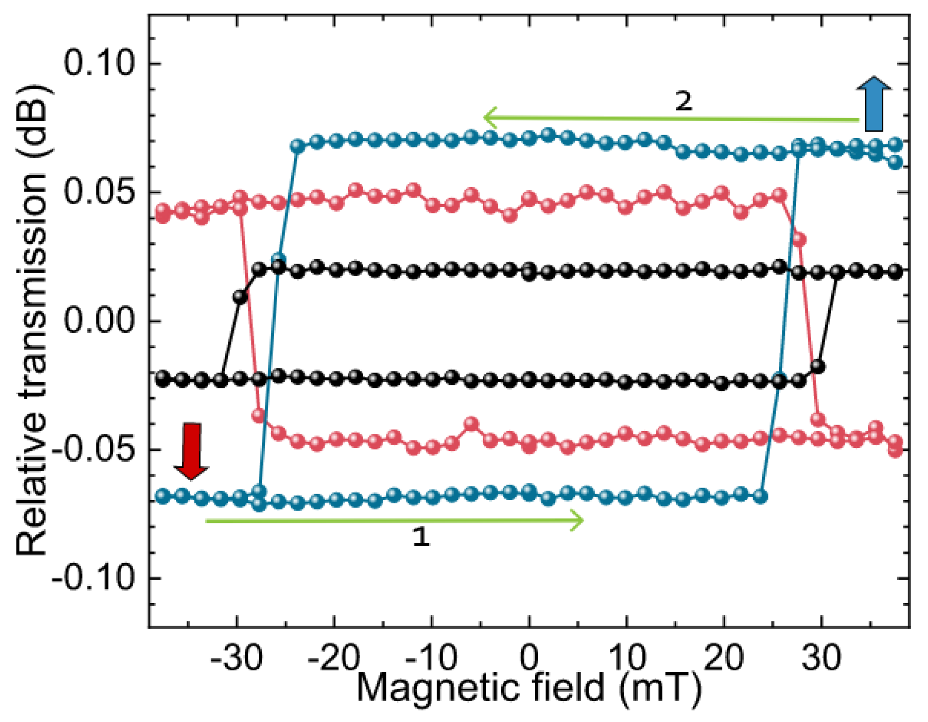
5.2. Co/Pt Magneto-Optical Kerr Effect (MOKE) Material

All-optical memory has been a topic in research for some time now [96,97]. Currently, photonic memory is vastly outperformed by the electronic memory. However, magnetic memory materials interact magneto-optically, which allows for optical memory functionality in photonic integrated circuits. On the InP membrane platform, a magneto-photonic device with a built-in, nano-scale magnetic memory bit applied to a standard optical waveguide is demonstrated [98]. A ferromagnetic, multilayered film (12 nm thickness) containing Co/Pt layers is applied as a top cladding, with perpendicular magnetic anisotropy [99]. Integration with a polarization converter can enlarge the sensitivity towards the relatively small polarization rotation introduced by the MO cladding. The device and intended operation of the device is shown in Figure 24.
The measured device shows hysteresis behavior when the magnetic field applied to the cladding is flipped. The resulting relative transmission, which is the measured difference when the magnetic field is flipped, is shown in Figure 25.
Devices with up to 1% optical transmission change are demonstrated with this principle, paving the way for photonic memory.

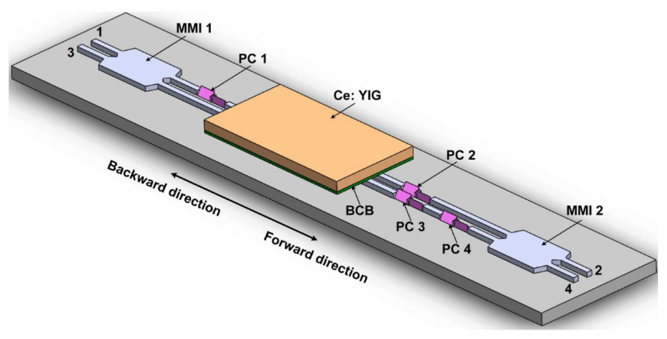
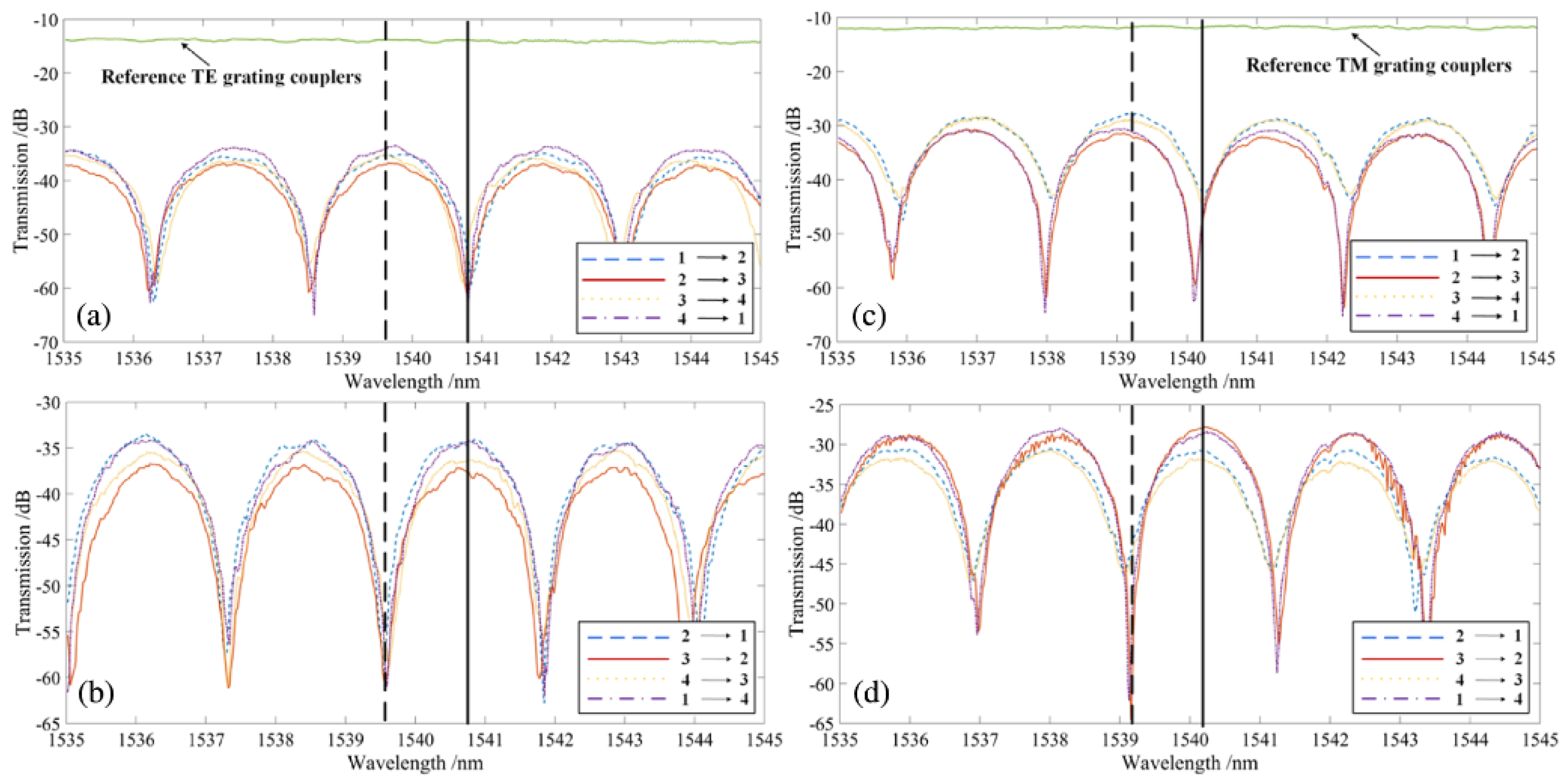
5.3. Yttrium Iron Garnet

Non-reciprocal optical components, such as optical isolators and circulators, are essential in optical communication systems. However, their integration with lasers and other optical components at the module level significantly increases packaging costs. Therefore, the challenge [100] of integration on the chip level is one that is desirable to overcome. Most integrated optical isolators and circulators rely on non-reciprocal phase shift (NRPS) [101]; however, non-reciprocal mode conversion (NRMC) has been given more attention, since it can function independently of the polarization of the light [102]. A non-reciprocal device was demonstrated on the InP membrane platform by connecting PCs with a MZI structure and adhesive bonding of a cerium-doped yttrium iron garnet (Ce:YIG) layer on the waveguide [103]. A schematic of the device is shown in Figure 26, the port numbers are indicated with numbers one to four for later reference.
The Ce:YIG is magnetized with an external magnet during characterization, with a magnetic field strength of 50 Oe, measured with a gauss-meter, which is strong enough to saturate the Ce:YIG. The transmission spectra are measured between port 2 and port 3 and vice versa, as shown in Figure 27. An isolation of 24.1 dB and 34.0 dB is measured for TE-mode and TM-mode light, respectively. This device can be used as a circulator, as shown by the spectra in Figure 28.

6. Conclusions

With the InP material system promising a complete component portfolio, various optical functions have been realized on the IMOS platform, spanning light generation, fast optical modulation and detection, polarization conversion, and mode manipulation. Several complex circuit demonstrations have been performed based on these basic building blocks. Example circuits include widely tunable lasers, mode-division multiplexed amplifiers, and dual-polarization lasers, which are conveniently realized through the native InP active–passive interface. Incorporating exotic materials further extends the platform’s capability, unlocking new opportunities such as optical non-reciprocity and magneto-optic functions. A summary of the key performance metrics for the building blocks presented in this paper is shown in Table 2.
State-of-the-art Si- and SiN-based platforms can also produce active–passive circuits by heterogeneous integration with InP or GaAs and electro-optic materials like LiNbO3 and BTO to further enhance the modulation speed. While the performances of some IMOS building blocks are still catching up with the best demonstrations on these Si-based platforms, the IMOS approach offers a versatile one-stop PIC solution that allows for easy interfacing with other technologies via wafer-level assembly. Performance scaling of active components is now explored through advanced heat management by thermal shunting and RF design optimizations. Double-sided processing on IMOS opens up new avenues to minimize the access resistance, as demonstrated with the UTC-PD of a beyond-110 GHz bandwidth. Active–passive integration on the same membrane also provides maximum design flexibility in component placement within the PIC. This is in contrast to InP-Si heterogeneous circuits realized by die-bonding, where inter-die mechanical conflicts have to be considered.
Advanced tooling and volume scaling are being incorporated into the IMOS technology. Wafer size expansion to 100 mm and industrial-grade ArF DUV lithography are now accelerating fast wafer iteration and yield learning. Such development is now further pushing the commercialization of IMOS, with open-access initiatives supported by PDKs and MPW shuttles offered through JePPIX.

Author Contributions

Conceptualization, S.R., Y.W. and Y.J.; writing—original draft preparation, S.R., Y.W., S.A., J.d.G. and A.Z.; writing—review and editing, S.R., Y.W., S.A., J.d.G., A.Z., K.W. and Y.J.; project administration, K.W. and Y.J.; funding acquisition, K.W. and Y.J. All authors have read and agreed to the published version of the manuscript.

Funding

This work was funded by the NWO Zwaartekracht Project “Research Centre for Integrated Nanophotonics,” the H2020 ICT TWILIGHT Project (Contract No. 781471) under the Photonics PPP, the Institute of Design, Optoelectronics and Sensing (IDEAS) Project INTENSE, the Huawei research grant HDMI, and the Dutch National Growth Fund PhotonDelta.

Conflicts of Interest

The authors declare no conflicts of interest.

References

  1. Miller, S.E. Integrated Optics: An Introduction. Bell Syst. Tech. J. 1969, 48, 2059–2069. [Google Scholar] [CrossRef]
  2. Wang, Y.; Jiao, Y.; Williams, K. Scaling photonic integrated circuits with InP technology: A perspective. APL Photonics 2024, 9, 050902. [Google Scholar] [CrossRef]
  3. Smit, M.; van der Tol, J.; Hill, M. Moore’s law in photonics. Laser Photonics Rev. 2012, 6, 1–13. [Google Scholar] [CrossRef]
  4. JePPIX Roadmap 2021–2025. Available online: https://www.jeppix.eu/about-us/roadmap-latest-edition (accessed on 1 July 2025).
  5. Soares, F.M.; Janiak, K.; Grote, N.; Szymanski, D.; Wale, M.J. Generic InP-Based Monolithic Photonic Integration Platforms. In Proceedings of the 18th European Conference on Integrated Optics, Warsaw, Poland, 18–20 May 2016. [Google Scholar]
  6. Smit, M.; Leijtens, X.; Ambrosius, H.; Bente, E.; van der Tol, J.; Smalbrugge, B.; de Vries, T.; Geluk, E.J.; Bolk, J.; van Veldhoven, R.; et al. An introduction to InP-based generic integration technology. Semicond. Sci. Technol. 2014, 29, 083001. [Google Scholar] [CrossRef]
  7. Galarza, M.; Van Thourhout, D.; Baets, R.; López-Amo, M. Compact and Highly-Efficient Vertical Couplers for Active-Passive Monolithic Integration. In Proceedings of the Integrated Photonics Research and Applications/Nanophotonics for Information Systems, San Diego, CA, USA, 10–13 April 2005; p. IWG3. [Google Scholar] [CrossRef]
  8. Marsh, J.H. Quantum well intermixing. Semicond. Sci. Technol. 1993, 8, 1136–1155. [Google Scholar] [CrossRef]
  9. Kulkova, I.; Kadkhodazadeh, S.; Kuznetsova, N.; Huck, A.; Semenova, E.; Yvind, K. High-quality MOVPE butt-joint integration of InP/AlGaInAs/InGaAsP-based all-active optical components. J. Cryst. Growth 2014, 402, 243–248. [Google Scholar] [CrossRef]
  10. Klamkin, J.; Zhao, H.; Song, B.; Liu, Y.; Isaac, B.; Pinna, S.; Sang, F.; Coldren, L. Indium Phosphide Photonic Integrated Circuits: Technology and Applications. In Proceedings of the 2018 IEEE BiCMOS and Compound Semiconductor Integrated Circuits and Technology Symposium (BCICTS), San Diego, CA, USA, 15–17 October 2018; pp. 8–13. [Google Scholar] [CrossRef]
  11. Zhang, K.; Burghart, D.; Gardanow, A.; Mayer, R.; Meyer, R.; Böhm, G.; Belkin, M.A. Mid-infrared integrated photonics on the InP platform. In Semiconductor Lasers and Laser Dynamics X; International Society for Optics and Photonics; SPIE: Bellingham, WA, USA, 2022; Volume PC12141, p. PC121410E. [Google Scholar] [CrossRef]
  12. Yan, Z.; Han, Y.; Lin, L.; Xue, Y.; Ma, C.; Ng, W.K.; Wong, K.S.; Lau, K.M. A monolithic InP/SOI platform for integrated photonics. Light. Sci. Appl. 2021, 10, 200. [Google Scholar] [CrossRef]
  13. Wada, H.; Kamijoh, T. Direct Bonding of InP to Si for Optoelectronic Integration. In Spatial Light Modulators; Optical Society of America: Washington, DC, USA, 1997; p. SMB.1. [Google Scholar] [CrossRef]
  14. Loi, R.; O’Callaghan, J.; Roycroft, B.; Quan, Z.; Thomas, K.; Gocalinska, A.; Pelucchi, E.; Trindade, A.J.; Bower, C.A.; Corbett, B. Thermal Analysis of InP Lasers Transfer Printed to Silicon Photonics Substrates. J. Light. Technol. 2018, 36, 5935–5941. [Google Scholar] [CrossRef]
  15. Jiao, Y.; Nishiyama, N.; van der Tol, J.J.; van Engelen, J.P.; Pogoretskiy, V.; Reniers, S.F.; Kashi, A.A.; Wang, Y.; Calzadilla, V.D.; Spiegelberg, M.; et al. InP membrane integrated photonics research. Semicond. Sci. Technol. 2020, 36, 013001. [Google Scholar] [CrossRef]
  16. Reniers, S.F.G.; Wang, Y.; Williams, K.A.; Van Der Tol, J.J.G.M.; Jiao, Y. Characterization of Waveguide Photonic Crystal Reflectors on Indium Phosphide Membranes. IEEE J. Quantum Electron. 2019, 55, 6400107. [Google Scholar] [CrossRef]
  17. Pello, J.; van der Tol, J.; Keyvaninia, S.; van Veldhoven, R.; Ambrosius, H.; Roelkens, G.; Smit, M. High-efficiency ultrasmall polarization converter in InP membrane. Opt. Lett. 2012, 37, 3711–3713. [Google Scholar] [CrossRef]
  18. Reniers, S.F.G.; Williams, K.A.; van der Tol, J.J.G.M.; Jiao, Y. An Accurate Characterization Method for Integrated Polarization Converters. IEEE J. Quantum Electron. 2021, 57, 0600306. [Google Scholar] [CrossRef]
  19. Reniers, S.F.G. Integration of a Polarization Converter on the Active-Passive IMOS Platform. Ph.D. Thesis, Eindhoven University of Technology, Eindhoven, The Netherlands, 2022. [Google Scholar]
  20. Hsu, C.P.; Li, B.; Solano-Rivas, B.; Gohil, A.R.; Chan, P.H.; Moore, A.D.; Donzella, V. A Review and Perspective on Optical Phased Array for Automotive LiDAR. IEEE J. Sel. Top. Quantum Electron. 2021, 27, 8300416. [Google Scholar] [CrossRef]
  21. Hutchison, D.N.; Sun, J.; Doylend, J.K.; Kumar, R.; Heck, J.; Kim, W.; Phare, C.T.; Feshali, A.; Rong, H. High-resolution aliasing-free optical beam steering. Optica 2016, 3, 887. [Google Scholar] [CrossRef]
  22. Wang, Y.; van Engelen, J.P.; Reniers, S.F.G.; Dolores-Calzadilla, V.; Williams, K.A.; Smit, M.K.; Jiao, Y. High resolution grating antennas for beam steering on the IMOS platform. In Proceedings of the 2019 Asia Communications and Photonics Conference, Chengdu, China, 2–5 November 2019. [Google Scholar]
  23. Wang, Y.; van Engelen, J.P.; Reniers, S.F.G.; van Rijn, M.B.J.; Zhang, X.; Cao, Z.; Dolores-Calzadilla, V.; Williams, K.A.; Smit, M.K.; Jiao, Y. InP-Based Grating Antennas for High-Resolution Optical Beam Steering. IEEE J. Sel. Top. Quantum Electron. 2021, 27, 6100107. [Google Scholar] [CrossRef]
  24. Wang, Y. InP Membrane Photonics for Large-Scale Integration. Ph.D. Thesis, Eindhoven University of Technology, Eindhoven, The Netherlands, 2023. [Google Scholar]
  25. Takahashi, N.; Wang, Y.; Nishiyama, N.; Williams, K.; Latkowski, S.; Jiao, Y. Compact widely-tunable laser on an InP membrane on silicon. In Proceedings of the 2023 Opto-Electronics and Communications Conference (OECC), Shanghai, China, 2–6 July 2023; pp. 1–2. [Google Scholar] [CrossRef]
  26. Kish, F.; Lal, V.; Evans, P.; Corzine, S.W.; Ziari, M.; Butrie, T.; Reffle, M.; Tsai, H.S.; Dentai, A.; Pleumeekers, J.; et al. System-on-Chip Photonic Integrated Circuits. IEEE J. Sel. Top. Quantum Electron. 2018, 24, 6100120. [Google Scholar] [CrossRef]
  27. Takahashi, N.; Fang, W.; Xue, R.; Katsumi, S.; Ohiso, Y.; Amemiya, T.; Nishiyama, N. Low Threshold Current Operation of Membrane DR Laser on Si with Buried-Ridge Waveguide and ACPM Grating for On-chip Optical Interconnection. In Proceedings of the 2022 28th International Semiconductor Laser Conference (ISLC), Matsue, Japan, 16–19 October 2022; pp. 1–2. [Google Scholar] [CrossRef]
  28. Matsuo, S.; Aihara, T.; Hiraki, T.; Maeda, Y.; Kishi, T.; Fujii, T.; Takeda, K.; Kakitsuka, T. Heterogeneously Integrated Membrane III-V Compound Semiconductor Devices with Silicon Photonics Platform. IEEE J. Sel. Top. Quantum Electron. 2022, 29, 6100510. [Google Scholar] [CrossRef]
  29. Pogoretskiy, V.; Van Engelen, J.; Van Der Tol, J.; Higuera-Rodriguez, A.; Smit, M.; Jiao, Y. An Integrated SOA-building block for an InP-membrane platform. In Proceedings of the Advanced Photonics 2017 (IPR, NOMA, Sensors, Networks, SPPCom, PS), New Orleans, LA, USA, 24–27 July 2017; p. JW4A.1. [Google Scholar] [CrossRef]
  30. Feyisa, D.W.; Abdi, S.; Van Veldhoven, R.; Calabretta, N.; Jiao, Y.; Stabile, R. Low Polarization Sensitive O-band SOA on InP Membrane for Advanced Photonic Integration. J. Light. Technol. 2024, 42, 4531–4541. [Google Scholar] [CrossRef]
  31. Zozulia, A.; Bolk, J.; Van Veldhoven, R.; Nazarikov, G.; Pogoretskiy, V.; Rihani, S.; Berry, G.; Williams, K.; Jiao, Y. Nanophotonic integrated active-passive InP membrane devices and circuits fabricated using ArF scanner lithography. Micro Nano Eng. 2024, 23, 100258. [Google Scholar] [CrossRef]
  32. Zozulia, A.; Schatz, R.; Rihani, S.; Berry, G.; Williams, K.; Jiao, Y. C-Band Directly Modulated Lasers With Tunable Photon–Photon Resonance in InP Membrane. IEEE J. Quantum Electron. 2024, 60, 2200312. [Google Scholar] [CrossRef]
  33. Pogoretskiy, V. Nanophotonic Membrane Platform for Integrated Active Devices and Circuits. Ph.D. Thesis, Eindhoven University of Technology, Eindhoven, The Netherlands, 2019. [Google Scholar]
  34. Grzeslo, M.; Dülme, S.; Clochiatti, S.; Neerfeld, T.; Haddad, T.; Lu, P.; Tebart, J.; Makhlouf, S.; Biurrun-Quel, C.; Fernández Estévez, J.L.; et al. High Saturation Photocurrent THz Waveguide-Type MUTC-photodiodes Reaching mW Output Power within the WR3.4 Band. Opt. Express 2023, 31, 6484. [Google Scholar] [CrossRef]
  35. Shen, L.; Jiao, Y.; Yao, W.; Cao, Z.; van Engelen, J.P.; Roelkens, G.; Smit, M.K.; van der Tol, J.J.G.M. High-bandwidth uni-traveling carrier waveguide photodetector on an InP-membrane-on-silicon platform. Opt. Express 2016, 24, 8290–8301. [Google Scholar] [CrossRef]
  36. de Graaf, J.; Zhao, X.; Konstantinou, D.; Hout, M.v.d.; Reniers, S.; Shen, L.; van der Heide, S.; Rommel, S.; Monroy, I.T.; Okonkwo, C.; et al. Beyond 110 GHz Uni-Traveling Carrier Photodiodes on an InP-Membrane-on-Silicon Platform. IEEE J. Sel. Top. Quantum Electron. 2022, 28, 3802010. [Google Scholar] [CrossRef]
  37. Maes, D.; Lemey, S.; Roelkens, G.; Zaknoune, M.; Avramovic, V.; Okada, E.; Szriftgiser, P.; Peytavit, E.; Ducournau, G.; Kuyken, B. High-speed uni-traveling-carrier photodiodes on silicon nitride. APL Photonics 2023, 8, 016104. [Google Scholar] [CrossRef]
  38. Lischke, S.; Peczek, A.; Morgan, J.S.; Sun, K.; Steckler, D.; Yamamoto, Y.; Korndörfer, F.; Mai, C.; Marschmeyer, S.; Fraschke, M.; et al. Ultra-fast germanium photodiode with 3-dB bandwidth of 265 GHz. Nat. Photonics 2021, 15, 925–931. [Google Scholar] [CrossRef]
  39. Cui, J.; Li, T.; Yang, F.; Cui, W.; Chen, H. The dual-injection Ge-on-Si photodetectors with high saturation power by optimizing light field distribution. Opt. Commun. 2021, 480, 126467. [Google Scholar] [CrossRef]
  40. Zhou, D.; Chen, G.; Fu, S.; Zuo, Y.; Yu, Y. Germanium photodetector with distributed absorption regions. Opt. Express 2020, 28, 19797. [Google Scholar] [CrossRef]
  41. Chang, C.M.; Sinsky, J.H.; Dong, P.; De Valicourt, G.; Chen, Y.K. High-power dual-fed traveling wave photodetector circuits in silicon photonics. Opt. Express 2015, 23, 22857. [Google Scholar] [CrossRef] [PubMed]
  42. Zhou, G.; Runge, P.; Keyvaninia, S.; Seifert, S.; Ebert, W.; Mutschall, S.; Seeger, A.; Li, Q.; Beling, A. High-Power InP-Based Waveguide Integrated Modified Uni-Traveling-Carrier Photodiodes. J. Light. Technol. 2017, 35, 717–721. [Google Scholar] [CrossRef]
  43. Rymanov, V.; Khani, B.; Dülme, S.; Lu, P.; Stöhr, A. InP-Based Waveguide Triple Transit Region Photodiodes for Hybrid Integration with Passive Optical Silica Waveguides. Photonics 2015, 2, 1152–1163. [Google Scholar] [CrossRef]
  44. Rouvalis, E.; Chtioui, M.; van Dijk, F.; Lelarge, F.; Fice, M.J.; Renaud, C.C.; Carpintero, G.; Seeds, A.J. 170 GHz uni-traveling carrier photodiodes for InP-based photonic integrated circuits. Opt. Express 2012, 20, 20090. [Google Scholar] [CrossRef]
  45. Xiao, F.; Han, Q.; Ye, H.; Wang, S.; Xiao, F. InP-based high-speed monolithic PIN photodetector integrated with an MQW semiconductor optical amplifier. Jpn. J. Appl. Phys. 2022, 61, 012005. [Google Scholar] [CrossRef]
  46. Anagnosti, M.; Caillaud, C.; Paret, J.F.; Pommereau, F.; Glastre, G.; Blache, F.; Achouche, M. Record Gain x Bandwidth (6.1 THz) Monolithically Integrated SOA-UTC Photoreceiver for 100-Gbit/s Applications. J. Light. Technol. 2015, 33, 1186–1190. [Google Scholar] [CrossRef]
  47. Anagnosti, M.; Caillaud, C.; Blache, F.; Jorge, F.; Angelini, P.; Paret, J.F.; Achouche, M. Optimized High Speed UTC Photodiode for 100 Gbit/s Applications. IEEE J. Sel. Top. Quantum Electron. 2014, 20, 29–35. [Google Scholar] [CrossRef]
  48. Caillaud, C.; Glastre, G.; Lelarge, F.; Brenot, R.; Bellini, S.; Paret, J.F.; Drisse, O.; Carpentier, D.; Achouche, M. Monolithic Integration of a Semiconductor Optical Amplifier and a High-Speed Photodiode With Low Polarization Dependence Loss. IEEE Photonics Technol. Lett. 2012, 24, 897–899. [Google Scholar] [CrossRef]
  49. Wang, Y.; Wei, Y.; Dolores-Calzadilla, V.; Dai, D.; Williams, K.; Smit, M.; Jiao, Y. Efficiency-boosted semiconductor optical amplifiers via mode-division multiplexing. Optica 2023, 10, 1153. [Google Scholar] [CrossRef]
  50. Wang, Y.; Dolores-Calzadilla, V.; Williams, K.; Smit, M. Efficient thermo-optic phase modulators on an indium phosphide membrane. In Proceedings of the 25th Annual Symposium of the IEEE Photonics Society Benelux, Mons, Belgium, 25–26 November 2021. [Google Scholar]
  51. Wang, Y.; Dolores-Calzadilla, V.; Williams, K.A.; Smit, M.K.; Jiao, Y. Ultra-Compact and Efficient Microheaters on a Submicron-Thick InP Membrane. J. Light. Technol. 2022, 41, 1790–1800. [Google Scholar] [CrossRef]
  52. Qiu, H.; Liu, Y.; Luan, C.; Kong, D.; Guan, X.; Ding, Y.; Hu, H. Energy-efficient thermo-optic silicon phase shifter with well-balanced overall performance. Opt. Lett. 2020, 45, 4806. [Google Scholar] [CrossRef]
  53. Chung, S.; Nakai, M.; Hashemi, H. Low-power thermo-optic silicon modulator for large-scale photonic integrated systems. Opt. Express 2019, 27, 13430. [Google Scholar] [CrossRef] [PubMed]
  54. Konoike, R.; Suzuki, K.; Namiki, S.; Kawashima, H.; Ikeda, K. Ultra-compact silicon photonics switch with high-density thermo-optic heaters. Opt. Express 2019, 27, 10332. [Google Scholar] [CrossRef] [PubMed]
  55. Sun, J.; Timurdogan, E.; Yaacobi, A.; Zhan, S.; Hosseini, E.S.; Cole, D.B.; Watts, M.R. Large-Scale Silicon Photonic Circuits for Optical Phased Arrays. IEEE J. Sel. Top. Quantum Electron. 2014, 20, 264–278. [Google Scholar] [CrossRef]
  56. Kashi, A.; van der Tol, J.; Williams, K.; Yao, W.; Lebby, M.S.; Pecinovsky, C.; Jiao, Y. Electro-Optic Slot Waveguide Phase Modulator on the InP Membrane on Silicon Platform. IEEE J. Quantum Electron. 2020, 57, 0600210. [Google Scholar] [CrossRef]
  57. Kashi, A.A. Electro-Optic Slot Waveguide Phase Modulators on the InP Membrane on Silicon Platform. Ph.D. Thesis, Eindhoven University of Technology, Eindhoven, The Netherlands, 2022. [Google Scholar]
  58. Kieninger, C.; Kutuvantavida, Y.; Elder, D.L.; Wolf, S.; Zwickel, H.; Blaicher, M.; Kemal, J.N.; Lauermann, M.; Randel, S.; Freude, W.; et al. Ultra-High Electro-Optic Activity Demonstrated in a Silicon-Organic Hybrid Modulator. Optica 2018, 5, 739. [Google Scholar] [CrossRef]
  59. Xu, M.; Cai, X. Advances in integrated ultra-wideband electro-optic modulators [Invited]. Opt. Express 2022, 30, 7253. [Google Scholar] [CrossRef]
  60. Sekine, N.; Toprasertpong, K.; Takagi, S.; Takenaka, M. Numerical analyses of optical loss and modulation bandwidth of an InP organic hybrid optical modulator. Opt. Express 2020, 28, 29730. [Google Scholar] [CrossRef]
  61. Eppenberger, M.; Messner, A.; Bitachon, B.I.; Heni, W.; Blatter, T.; Habegger, P.; Destraz, M.; De Leo, E.; Meier, N.; Del Medico, N.; et al. Resonant plasmonic micro-racetrack modulators with high bandwidth and high temperature tolerance. Nat. Photonics 2023, 17, 360–367. [Google Scholar] [CrossRef]
  62. Horst, Y.; Moor, D.; Chelladurai, D.; Blatter, T.; Fernandes, S.; Kulmer, L.; Baumann, M.; Ibili, H.; Funck, C.; Keller, K.; et al. Ultra-Wideband MHz to THz Plasmonic EO Modulator. Optica 2025, 12, 325. [Google Scholar] [CrossRef]
  63. Xiang, C.; Jin, W.; Terra, O.; Dong, B.; Wang, H.; Wu, L.; Guo, J.; Morin, T.J.; Hughes, E.; Peters, J.; et al. 3D Integration Enables Ultralow-Noise Isolator-Free Lasers in Silicon Photonics. Nature 2023, 620, 78–85. [Google Scholar] [CrossRef]
  64. Rahim, A.; Baets, R.G. Heterogeneous Integration in Silicon Photonics: Opportunities and Challenges: Opinion. Opt. Mater. Express 2023, 13, 3439–3444. [Google Scholar] [CrossRef]
  65. Arafin, S.; Coldren, L.A. Advanced InP Photonic Integrated Circuits for Communication and Sensing. IEEE J. Sel. Top. Quantum Electron. 2018, 24, 6100612. [Google Scholar] [CrossRef]
  66. Spiegelberg, M. 3D-Integration on Wafer Level of Photonic and Electronic Circuits. Ph.D. Thesis, Technische Universiteit Eindhoven, Eindhoven, The Netherlands, 2021. [Google Scholar]
  67. Abdi, S.; de Vries, T.; Spiegelberg, M.; Williams, K.; Jiao, Y. Novel wafer-scale adhesive bonding with improved alignment accuracy and bond uniformity. Microelectron. Eng. 2023, 270, 111936. [Google Scholar] [CrossRef]
  68. Wang, X.; Niklaus, F. 3D and Circuit Integration of MEMS; John Wiley & Sons: Hoboken, NJ, USA, 2021. [Google Scholar]
  69. Zhang, X.; Liu, X.; Spiegelberg, M.; Van Dommele, A.R.; Matters-Kammerer, M.K. A DC-51.5 GHz Electro-Absorption Modulator Driver with Tunable Differential DC Coupling for 3D Wafer Scale Packaging. In Proceedings of the 2019 IEEE BiCMOS and Compound semiconductor Integrated Circuits and Technology Symposium (BCICTS), Nashville, TN, USA, 3–6 November 2019; pp. 1–4. [Google Scholar] [CrossRef]
  70. Abdi, S.; De Vries, T.; Spiegelberg, M.; Williams, K.; Jiao, Y. Wafer-scale adhesive bonding with hard Benzocyclobutene anchors for wafer assembly and heterogeneous integration. In Proceedings of the 2023 34th Annual SEMI Advanced Semiconductor Manufacturing Conference (ASMC), Saratoga Springs, NY, USA, 1–4 May 2023; pp. 1–4. [Google Scholar] [CrossRef]
  71. Abdi, S.; Zozulia, A.; Bolk, J.; Geluk, E.J.; Williams, K.; Jiao, Y. Study of Spatial Distortion in InP Nanophotonic Membranes on Different Carrier Substrates. In Proceedings of the 2023 24th European Microelectronics and Packaging Conference & Exhibition (EMPC), Cambridge, UK, 11–14 September 2023; pp. 1–5. [Google Scholar] [CrossRef]
  72. Liu, F.; Nimbalkar, P.; Aslani-Amoli, N.; Kathaperumal, M.; Tummala, R.; Swaminathan, M. A Critical Review of Lithography Methodologies and Impacts of Topography on 2.5-D/3-D Interposers. IEEE Trans. Components, Packag. Manuf. Technol. 2023, 13, 291–299. [Google Scholar] [CrossRef]
  73. Lau, J.H. Recent Advances and Trends in Advanced Packaging. IEEE Trans. Components, Packag. Manuf. Technol. 2022, 12, 228–252. [Google Scholar] [CrossRef]
  74. Wang, Y.; Wei, Y.; Dolores-Calzadilla, V.; Williams, K.; Smit, M.; Dai, D.; Jiao, Y. Mode division multiplexing on an InP membrane on silicon. Opt. Lett. 2022, 47, 4004. [Google Scholar] [CrossRef]
  75. Dai, D.; Li, C.; Wang, S.; Wu, H.; Shi, Y.; Wu, Z.; Gao, S.; Dai, T.; Yu, H.; Tsang, H. 10-Channel Mode (de)multiplexer with Dual Polarizations. Laser Photonics Rev. 2018, 12, 1700109. [Google Scholar] [CrossRef]
  76. Huang, H.; Han, X.; Balčytis, A.; Dubey, A.; Boes, A.; Nguyen, T.G.; Ren, G.; Tan, M.; Tian, Y.; Mitchell, A. Non-resonant recirculating light phase modulator. APL Photonics 2022, 7, 106102. [Google Scholar] [CrossRef]
  77. Zhang, K.; Sun, W.; Chen, Y.; Feng, H.; Zhang, Y.; Chen, Z.; Wang, C. A power-efficient integrated lithium niobate electro-optic comb generator. Commun. Phys. 2023, 6, 17. [Google Scholar] [CrossRef]
  78. Miller, S.A.; Chang, Y.C.; Phare, C.T.; Shin, M.C.; Zadka, M.; Roberts, S.P.; Stern, B.; Ji, X.; Mohanty, A.; Jimenez Gordillo, O.A.; et al. Large-scale optical phased array using a low-power multi-pass silicon photonic platform. Optica 2020, 7, 3. [Google Scholar] [CrossRef]
  79. Haverkort, J.E.M.; Dorren, B.H.P.; Kemerink, M.; Silov, A.Y.; Wolter, J.H. Design of composite InAsP/InGaAs quantum wells for a 1.55 μm polarization independent semiconductor optical amplifier. Appl. Phys. Lett. 1999, 75, 2782–2784. [Google Scholar] [CrossRef]
  80. Zali, A.R.; Kleijn, S.; Augustin, L.; Tessema, N.M.; Prifti, K.; Stabile, R.; Calabretta, N. Design and Fabrication of Low Polarization Dependent Bulk SOA Co-Integrated With Passive Waveguides for Optical Network Systems. J. Light. Technol. 2022, 40, 1083–1091. [Google Scholar] [CrossRef]
  81. Felicetti, M.; van der Tol, J.J.G.M.; Geluk, E.J.; Pustakhod, D.; Wale, M.J.; Smit, M.K. Integrated High-Performance TE/TM Converters for Polarization Independence in Semiconductor Optical Amplifiers. J. Light. Technol. 2015, 33, 3584–3590. [Google Scholar] [CrossRef]
  82. Augustin, L.M.; van der Tol, J.J.G.M.; Geluk, E.J.; Oei, Y.; Smit, M.K. Method for polarization effect suppression in semiconductor optical amplifiers. In Proceedings of the 14th European Conference on Integrated Optics (ECIO), Eindhoven, The Netherlands, 11–13 June 2008; p. 4. [Google Scholar]
  83. Newkirk, M.; Miller, B.; Koren, U.; Young, M.; Chien, M.; Jopson, R.; Burrus, C. 1.5 μm multiquantum-well semiconductor optical amplifier with tensile and compressively strained wells for polarization-independent gain. IEEE Photonics Technol. Lett. 1993, 5, 406–408. [Google Scholar] [CrossRef]
  84. Morito, K.; Ekawa, M.; Watanabe, T.; Kotaki, Y. High-output-power polarization-insensitive semiconductor optical amplifier. J. Light. Technol. 2003, 21, 176–181. [Google Scholar] [CrossRef]
  85. Reniers, S.; Williams, K.; Van Der Tol, J.; Jiao, Y. Integration of an Ultra-Short Polarization Rotator on an Active-Passive Indium Phosphide Membrane. In Proceedings of the 2023 Opto-Electronics and Communications Conference (OECC), Shanghai, China, 2–6 July 2023; pp. 1–5. [Google Scholar] [CrossRef]
  86. Latkowski, S.; Hansel, A.; Bhattacharya, N.; De Vries, T.; Augustin, L.; Williams, K.; Smit, M.; Bente, E. Novel Widely Tunable Monolithically Integrated Laser Source. IEEE Photonics J. 2015, 7, 1503709. [Google Scholar] [CrossRef]
  87. Kabir, T.; Wang, Y.; Tondini, S.; Williams, K.; Jiao, Y.; Heck, M.J.R. Compact widely tunable laser integrated on an indium phosphide membrane platform. Appl. Phys. Lett. 2024, 125, 121110. [Google Scholar] [CrossRef]
  88. Pajkovic, R.; Reep, T.; Williams, K.; Bente, E. Data-driven model to extend tuning range: From 1474 nm to 1568 nm in a monolithic laser. In Proceedings of the 2021 27th International Semiconductor Laser Conference (ISLC), Potsdam, Germany, 10–14 October 2021; pp. 1–2. [Google Scholar] [CrossRef]
  89. Zhang, H.; Gu, M.; Jiang, X.D.; Thompson, J.; Cai, H.; Paesani, S.; Santagati, R.; Laing, A.; Zhang, Y.; Yung, M.H.; et al. An optical neural chip for implementing complex-valued neural network. Nat. Commun. 2021, 12, 457. [Google Scholar] [CrossRef]
  90. Eldredge, J.G.; Hutchings, B.L. Density Enhancement of a Neural Network Using FPGAs and Run-Time Reconguration. In Proceedings of the Proceedings of IEEE Workshop on FPGA’s for Custom Computing Machines, Napa Valley, CA, USA, 10–13 April 1994. [Google Scholar]
  91. Lu, L.; Zhao, S.; Zhou, L.; Li, D.; Li, Z.; Wang, M.; Li, X.; Chen, J. 16 × 16 non-blocking silicon optical switch based on electro-optic Mach-Zehnder interferometers. Opt. Express 2016, 24, 9295. [Google Scholar] [CrossRef] [PubMed]
  92. Feldmann, J.; Youngblood, N.; Wright, C.D.; Bhaskaran, H.; Pernice, W.H.P. All-optical spiking neurosynaptic networks with self-learning capabilities. Nature 2019, 569, 208–214. [Google Scholar] [CrossRef]
  93. Teo, T.Y.; Krbal, M.; Mistrik, J.; Prikryl, J.; Lu, L.; Simpson, R.E. Comparison and analysis of phase change materials-based reconfigurable silicon photonic directional couplers. Opt. Mater. Express 2022, 12, 606. [Google Scholar] [CrossRef]
  94. Liu, H.; Dong, W.; Wang, H.; Lu, L.; Ruan, Q.; Tan, Y.S.; Simpson, R.E.; Yang, J.K.W. Rewritable color nanoprints in antimony trisulfide films. Sci. Adv. 2020, 6, eabb7171. [Google Scholar] [CrossRef]
  95. Lu, L.; Reniers, S.F.G.; Wang, Y.; Jiao, Y.; Simpson, R.E. Reconfigurable InP waveguide components using the Sb2 S3 phase change material. J. Opt. 2022, 24, 094001. [Google Scholar] [CrossRef]
  96. Li, X.; Youngblood, N.; Ríos, C.; Cheng, Z.; Wright, C.D.; Pernice, W.H.; Bhaskaran, H. Fast and reliable storage using a 5 bit, nonvolatile photonic memory cell. Optica 2019, 6, 1. [Google Scholar] [CrossRef]
  97. Tsakyridis, A.; Alexoudi, T.; Miliou, A.; Pleros, N.; Vagionas, C. 10 Gb/s optical random access memory (RAM) cell. Opt. Lett. 2019, 44, 1821. [Google Scholar] [CrossRef]
  98. Demirer, F.E.; Baron, Y.; Reniers, S.; Pustakhod, D.; Lavrijsen, R.; Van Der Tol, J.; Koopmans, B. An integrated photonic device for on-chip magneto-optical memory reading. Nanophotonics 2022, 11, 3319–3329. [Google Scholar] [CrossRef]
  99. Weller, D.; Brändle, H.; Gorman, G.; Lin, C.J.; Notarys, H. Magnetic and magneto-optical properties of cobalt-platinum alloys with perpendicular magnetic anisotropy. Appl. Phys. Lett. 1992, 61, 2726–2728. [Google Scholar] [CrossRef]
  100. Jalas, D.; Petrov, A.; Eich, M.; Freude, W.; Fan, S.; Yu, Z.; Baets, R.; Popović, M.; Melloni, A.; Joannopoulos, J.D.; et al. What is—And what is not—An optical isolator. Nat. Photonics 2013, 7, 579–582. [Google Scholar] [CrossRef]
  101. Stadler, B.J.H.; Mizumoto, T. Integrated Magneto-Optical Materials and Isolators: A Review. IEEE Photonics J. 2014, 6, 0600215. [Google Scholar] [CrossRef]
  102. Firby, C.J.; Chang, P.; Helmy, A.S.; Elezzabi, A.Y. Versatile broadband polarization-independent optical circulators for nanophotonic integrated circuits. J. Opt. Soc. Am. B 2018, 35, 1504. [Google Scholar] [CrossRef]
  103. Ma, R.; Reniers, S.; Shoji, Y.; Mizumoto, T.; Williams, K.; Jiao, Y.; van der Tol, J. Integrated polarization-independent optical isolators and circulators on an InP membrane on silicon platform. Optica 2021, 8, 1654. [Google Scholar] [CrossRef]
Figure 1. Schematic cross-section of the InP membrane platform. The active core consists of four InGaAsP multiple quantum wells (MQWs).
Chips 04 00032 g001
Figure 2. Three-dimensional mock of a photonic crystal reflector.
Chips 04 00032 g002
Figure 3. Spectrum of PhC reflector for various number of holes (N).
Chips 04 00032 g003
Figure 4. Schematic of a polarization converter on the IMOS platform.
Chips 04 00032 g004
Figure 5. (a) Cross-sectional schematic of the grating antenna. (b) Measured far-field emission of the grating antenna (black) and the Gaussian fitted profile (red).
Chips 04 00032 g005
Figure 6. Cross-section of the laser/SOA after bonding and schematic of the active–passive interface. (a,b) Twin-guide IMOS [29]; (c) IMOS with butt-joint integration [31].
Chips 04 00032 g006
Figure 7. (a) Schematic of a DFB laser; (b) SEM image featuring the λ /4 shift [33]. (c,d) LIV curve and optical spectrum at 55 mA of a 400 µm long and 1 µm wide DFB laser. (e) Small signal response measured for DFB lasers of different lengths.
Chips 04 00032 g007
Figure 8. The realized photonic crystal DBR laser with SEM images of the photonic crystal reflectors. The SOA length and width are 600 µm and 1.7 µm, respectively [33].
Chips 04 00032 g008
Figure 9. (a) Three-dimensional schematic depiction of the UTC-PD structure. (b) Opto-electric bandwidth of a 10 µm2 UTC-PD with a 3 dB bandwidth beyond 110 GHz at −4 V. (c) Microscope image of a UTC-PD integrated with an optical waveguide and an RF choke.
Chips 04 00032 g009
Figure 10. Bandwidth responsivity numbers reported on platform-integrated PDs, including performance prediction in the case of IMOS UTC-PD + SOA integration. All measurements have been carried out at C-band wavelengths.
Chips 04 00032 g010
Figure 11. Design of phase shifters on the IMOS platform (not-to-scale). (a): Cross-section of the metal-strip-based TOPS. (b): 3D illustration of the microheater with direct waveguide heating.
Chips 04 00032 g011
Figure 12. Performance of the microheater with direct waveguide heating. (a): Optical transmission as a function of heating power measured at different wavelengths. (b): Transient response of the microheater when heating power jumps from 0 to Pπ.
Chips 04 00032 g012
Figure 13. (a): Cross-section of the InP slot waveguide modulator. (b): Measured high-speed electro-optic response of the slot waveguide modulator.
Chips 04 00032 g013
Figure 14. (a) Cross-sectional schematic showing the integration of PIC and EIC. (b) Microscope image of an electronic–photonic integrated InP EML transmitter [66].
Chips 04 00032 g014
Figure 15. Wafer-to-wafer bonding with anchors. (a) pre-bonding. (b) BCB reflow and bonding. (c) after BCB curing. (d) cross-sectional SEM image of the post-bonding interface with BCB anchors [67].
Chips 04 00032 g015
Figure 16. Efficiency-boosted DP-SOA on the InP membrane platform [49]. (a) Top-view schematics of the DP-SOA. (b) Enhanced optical gain of the DP-SOA as compared to single-pass T E 0 , single-pass T E 1 , and the total of single-pass T E 0 and T E 1 .
Chips 04 00032 g016
Figure 17. Schematic of the polarization-independent SOA. L is the length of the SOA. If the original polarization state is required, an extra PC can be added before the first SOA section or after the second SOA section.
Chips 04 00032 g017
Figure 18. Polarization-dependent gain for injection currents up to 50 mA per SOA section and wavelengths between 1570 nm and 1600 nm. (a) The PDG of a standard SOA. (b) The PDG for a polarization-independent semiconductor optical amplifier (PI-SOA). Note that the measurements for 1590 nm and 1600 nm suffer from high losses from the surface grating couplers.
Chips 04 00032 g018
Figure 19. Schematic of a dual-polarization light source. Components include photonic crystal reflectors (PhCs), a semiconductor optical amplifier (SOA), a polarization converter (PC), and TE and TM output couplers.
Chips 04 00032 g019
Figure 20. SEM image of the fabricated circuit of a dual-polarization light source. Shown are the polarization converter (a), active–passive taper (b), and SOA (c).
Chips 04 00032 g020
Figure 21. (a): Microscope image of a fabricated tunable laser on IMOS. (b): Measured spectra in fiber. The coupling loss is around 10 dB. (c): Microscope image of a fabricated tunable laser on IMOS. (d): Measured spectra in fiber. The coupling loss is around 10 dB.
Chips 04 00032 g021
Figure 22. Microscope image of the MZI device [95].
Chips 04 00032 g022
Figure 23. Transmission spectrum for a reconfigurable MZI. (a) Simulated spectrum. (b) Measured spectrum before and after crystallization with 7.5 mW, 50 ms laser pulses with a wavelength of 658 nm [95].
Chips 04 00032 g023
Figure 24. (a) Schematic of the magnetic memory. (b,c) Poincaré sphere representation of the device [98].
Chips 04 00032 g024
Figure 25. The relative transmission of the device is shown for various lengths of triangular and rectangular sections. A hysteresis effect is observed when swapping from positive to negative field strengths.
Chips 04 00032 g025
Figure 26. Schematic of the integrated optical circulator [103].
Chips 04 00032 g026
Figure 27. Transmission spectra between port 2 and port 3 for (a) TE-mode light and (b) TM-mode light.
Chips 04 00032 g027
Figure 28. Transmission spectra for different circulating directions for TE-mode input in (a) the clockwise direction and (b) the counterclockwise direction. And for TM mode input in (c) the clockwise direction and (d) the counterclockwise direction.
Chips 04 00032 g028
Table 1. Obtained reflectivity of a PhC reflector with a Fabry–Pérot and direct 4-port measurement method. Simulated values shown for comparison.
Number of HolesR (FP Method)R (Direct Method)R (Simulated)
50.8710.9020.932
70.9320.9680.972
90.9440.9900.991
Table 2. Summary of key performance metrics for building blocks and integrated sub-circuits discussed in this paper.
Building Block/Sub-CircuitPerformance MetricPerformance
PhC reflector [16]Reflectivity [%]99.0%
Polarization converter [18]Conversion efficiency97%
Optical antenna [23]Beam width0.05° FWHM
Optical antenna [23]Steering angle>13°
Directly modulated laser [32]Modulation bandwidth21 GHz
UTC PD [36]Bandwidth>110 GHz
TO phase shifter [50]Power efficiency2.2 mW/ π
TO phase shifter [50]Time constant13 µs
EO polymer modulator [56] V π L 3.9 Vmm
EO polymer modulator [56]Modulation bandwidth37 GHz
Double-pass SOA [49]WPE enhancement300% w.r.t. single-pass SOA
PI-SOA [19]PDG<3 dB
Tuneable membrane laser [87]Tuning range50 nm
Optical isolator [103]Isolation24.1 dB (TE), 34.0 dB (TM)
Disclaimer/Publisher’s Note: The statements, opinions and data contained in all publications are solely those of the individual author(s) and contributor(s) and not of MDPI and/or the editor(s). MDPI and/or the editor(s) disclaim responsibility for any injury to people or property resulting from any ideas, methods, instructions or products referred to in the content.

