Review

Advanced Doherty Power Amplifier Architectures for 5G Handset Applications: A Comprehensive Review of Linearity, Back-Off Efficiency, Bandwidth, and Thermal Management

by
Shihai He
* and
Huan Chen
Beijing Onmicro Electronics Co., Ltd., Beijing 100193, China
*
Author to whom correspondence should be addressed.
Chips 2025, 4(2), 20; https://doi.org/10.3390/chips4020020
Submission received: 3 March 2025 / Revised: 26 April 2025 / Accepted: 28 April 2025 / Published: 6 May 2025
(This article belongs to the Special Issue IC Design Techniques for Power/Energy-Constrained Applications)

Abstract

:
This paper presents a comprehensive review of GaAs HBT-based Doherty power amplifiers (DPAs) targeting 5G New Radio (NR) handset applications. Focusing on the critical challenges of linearity enhancement, back-off efficiency improvement, bandwidth extension under low-voltage (3.4 V) operation, and chip thermal management, the authors analyze state-of-the-art DPAs published in recent years. Key innovations including dynamic power division technique, third order intermodulation (IM3) cancellation technology, and compact output combiners are comparatively studied. Using 5G NR signals, the critical performance of the latest reported PA such as maximum linear power, back-off efficiency, bandwidth, and operating voltage are quantitatively investigated. The measurement results demonstrated that the best performance in recent DPAs achieved high linear power of 31 dBm with 34% PAE and 30 dBm with 31% PAE at the N78 and N77 bands, respectively. The corresponding adjacent channel leakage ratios (ACLRs) were lower than −36.5 dBc without digital pre-distortion (DPD). This review provides a comprehensive understanding of the latest advancements and future directions in highly efficient and linear DPA designs for 5G handset front-end modules.

1. Introduction

The transition to 5G NR with up to 100 MHz bandwidth and 12 dB peak-to-average power ratio (PAPR) imposes stringent demands on handset power amplifier (PA) designs. While envelope tracking (ET) has dominated the 4G LTE era, its bandwidth is a critical limitation of 5G. Recent studies have shown that Doherty PAs (DPAs) exhibit comparable system efficiency to ET PAs when operating with 100 MHz 256QAM signals [1,2,3,4]. It is well known that the efficiency of Envelope Tracking Power Amplifiers (ET PAs) depends not only on the amplifiers themselves, but also on the operational efficiency and maximum bandwidth of their envelope tracking modules. And, the implementation of ET technology incurs higher costs due to its requirement for additional power management ICs, while DPAs maintain compatibility with existing infrastructure, resulting in lower implementation costs. This advantage stems from the DPA’s intrinsic load modulation mechanism rather than external supply adjustment. However, due to the stringent requirements for linearity, back-off efficiency, bandwidth, and thermal management, three fundamental challenges persist in DPA designs for 5G handsets:
(1)
Nonlinear Phase Distortion from Asymmetric AM-AM/AM-PM Responses of Class-AB and Class-C Amplifiers
In a Doherty power amplifier (DPA) configuration, the carrier amplifier is typically designed to operate in Class-AB mode, which provides a balance between linearity and efficiency. However, this operational mode introduces gain compression as the input power increases, leading to a nonlinear relationship between input and output power levels. Conversely, the peaking amplifier is designed to operate in Class-C mode, which allows for higher efficiency at the cost of linearity, often resulting in gain expansion. This inherent asymmetry between the two amplifiers leads to significant amplitude and phase distortion.
The resulting nonlinear characteristics manifest in two key ways: amplitude modulation to amplitude modulation (AM–AM) distortion and amplitude modulation to phase modulation (AM–PM) distortion [5]. AM–AM distortion affects the output power in relation to the input power, causing deviations from the ideal linear response. Similarly, AM–PM distortion introduces phase shifts that can adversely affect signal integrity, particularly in communication systems that rely on precise phase information, such as 5G New Radio (NR). To mitigate these nonlinear distortions, advanced techniques have been developed. One effective approach is to implement dynamic power division strategies, where the power distribution between the carrier and peaking amplifiers is adjusted in real time based on the input signal conditions [1,2,3]. Additionally, harmonic suppression techniques can be employed to manipulate the amplifier’s harmonic responses, aligning the phase relationships of the intermodulation distortion components from both amplifiers to enhance cancellation effects. These strategies not only improve the linearity of the DPA, but also ensure that the overall system meets the stringent Adjacent Channel Leakage Ratio (ACLR) requirements essential for 5G applications.
(2)
Efficiency and Bandwidth Degradation Under 3.4 V Supply Compared to Traditional 5 V Systems
The transition to lower supply voltages such as 3.4 V in modern 5G handsets brings significant challenges for both efficiency and bandwidth in Doherty amplifiers. Firstly, the reduced supply voltage limits the output voltage swing, leading to a decrease in both the maximum output power and the overall efficiency of the amplifier compared to traditional 5 V systems [3]. For a given power output, as the peak voltage is reduced, the corresponding current must increase. This lowering of load impedance leads to the second contribution to performance reduction: lower load impedance bring higher loss as transformation ratio is increased. Accordingly, bandwidth is almost always compromised as load impedances are lowered. To address these efficiency and bandwidth challenges, several innovative strategies are being explored. One approach is the optimization of output-matching networks to enhance bandwidth at lower supply voltages [4,6]. Techniques such as adaptive bias control can also be employed, where the biasing of the amplifier is dynamically adjusted based on the input power level [7,8,9]. This ensures that the amplifier operates in the most efficient region of its performance characteristics, even at reduced supply voltages.
On the other hand, the efficiency-optimized design relies on precise impedance transformations between the carrier and peaking amplifier paths, which are inherently frequency-sensitive. Specifically, the quarter-wave transformers and compensating networks required for proper load modulation exhibit narrowband characteristics, restricting the operating bandwidth [10,11,12].
(3)
Thermal Management in Chips
Effective thermal management is critical for maintaining the reliability and performance of Doherty amplifiers in 5G applications. High power levels can lead to significant heat generation, which, if not managed properly, can adversely affect amplifier performance and longevity. Chip thermal management typically involves both die-level and system-level approaches. At the die level, layout optimization is required to balance thermal performance and cost. At the system level, it is necessary to compare the differences in overall thermal dissipation between flip-chip and wire-bond packaging processes. Through optimized layout design and advanced chip integration techniques, the overall thermal management of the chip can be effectively enhanced, consequently improving its comprehensive performance and reliability [13,14,15,16].
In conclusion, addressing these fundamental challenges—nonlinear amplitude/phase distortion, bandwidth restrictions, efficiency degradation, and thermal management—requires a multi-faceted approach involving innovative design strategies, advanced circuit techniques, and thorough performance optimization. By overcoming these obstacles, next-generation Doherty power amplifiers can meet the stringent requirements of 5G handsets, paving the way for more efficient and effective communication systems.

2. Key Technology Discussion

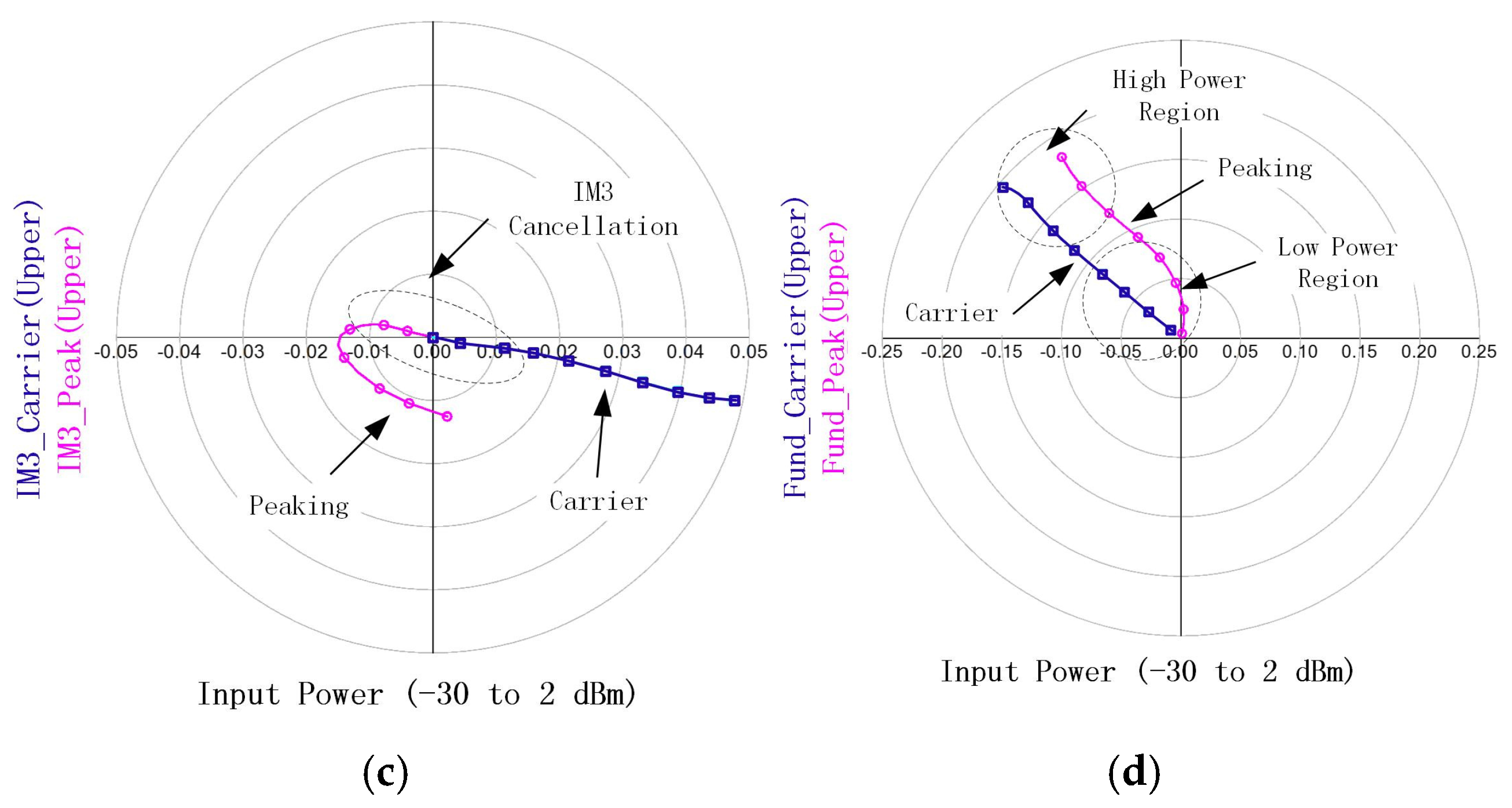
2.1. Linearity Enhancement Techniques

(1) IM3 Cancellation Techniques:
Cancellation of the third-order inter-modulation distortions (IMD3s) generated by the carrier and peaking amplifiers is the most important design issue in realizing a linear Doherty power amplifier [1,2]. The IM3 and fundamental signal of class AB biased carrier amplifier are in anti-phase when gain compression occurs. By contrast, the IM3 and fundamental signal of class B/C biased peaking amplifier are in phase at the beginning of gain expansion. Thus, the IM3s of the two amplifiers can cancel each other in specific power region to improve the linearity of the Doherty amplifier.
However, due to the RF swing controlled parasitic parameters in GaAs HBT, the phases of IM3 and fundamental signals from carrier and peaking amplifier deviate with input signal. For the linearity of this power amplifier, the π-shaped equivalent circuits of λ/4 transmission lines are optimized to compensate the phases of IM3s for cancellation. Meanwhile, bias-controlled PDR is designed to compensate the magnitude of IM3 for cancellation. To validate this theory, a two-tone signal with 100 MHz space was applied in a simulation. Figure 1a,b show that IM3s of carrier and peaking power amplifier have opposite phases from low to moderate signal levels. On the other hand, as shown in Figure 1c,d, the fundamental carrier and peaking power amplifier signals present some phase offsets (40 degree) at a low signal level, but a small deviation (16 degree) in the high power region. It is a trade-off between linearity and PAE. Considering the priority of IM3 cancellation, this optimization is acceptable.
(2) Adaptive Power Division:
Adaptive power division is a key innovation that facilitates flattening of the AM–AM characteristic across a wide input power range. By dynamically adjusting the power-dividing ratio (PDR) based on the input signal conditions, the carrier and peaking amplifiers can be optimized to operate in their most linear regions [1,2,3,4]. This is particularly important for reducing the distortion associated with gain compression and expansion in the two amplifiers. The implementation of real-time monitoring and control systems allows for continuous adjustment of the power division, ensuring optimal performance regardless of varying signal conditions. As shown in Figure 2, the bias-controlled PDR technique has a large and accurate dynamic range. This adaptability is vital for maintaining linearity in the context of 5G signals, which often exhibit high peak-to-average power ratios (PAPRs) and complex modulation schemes. In recent research on linear Doherty PAs, this technique has been widely adopted.

2.2. Back-Off Efficiency Improvement

The inherent design of the Doherty amplifier allows for improved efficiency at power back-off (PBO) levels due to its load modulation characteristics. As the input power decreases, the peaking amplifier is progressively disengaged, allowing the carrier amplifier to operate more efficiently under lower power conditions. This dynamic adjustment of load impedance enables the DPA to maintain higher efficiency compared to conventional amplifiers, which often suffer from significant efficiency drops at back-off levels. Recent designs have focused on optimizing the asymmetry between the carrier and peaking amplifiers to enhance efficiency even further. By fine-tuning the bias points and operating conditions of each amplifier, it is possible to achieve a broader range of efficient operation while minimizing distortion. In addition, three-way Doherty configuration is a typical back-off efficiency improvement technique.
(1)
Asymmetric Power Cell Designs:
The development of asymmetric power cell designs has proven effective in maximizing efficiency [5]. By configuring the carrier amplifier to operate in Class-AB mode and the peaking amplifier in a deeper Class-C bias, the overall efficiency at PBO can be significantly improved. This configuration allows the peaking amplifier to activate only when necessary, thus conserving power during lower output scenarios. In addition, the asymmetric power cell architecture, when integrated with the PDR technique mentioned earlier, enables superior IM3 interference cancellation, leading to enhanced linearity performance.
(2)
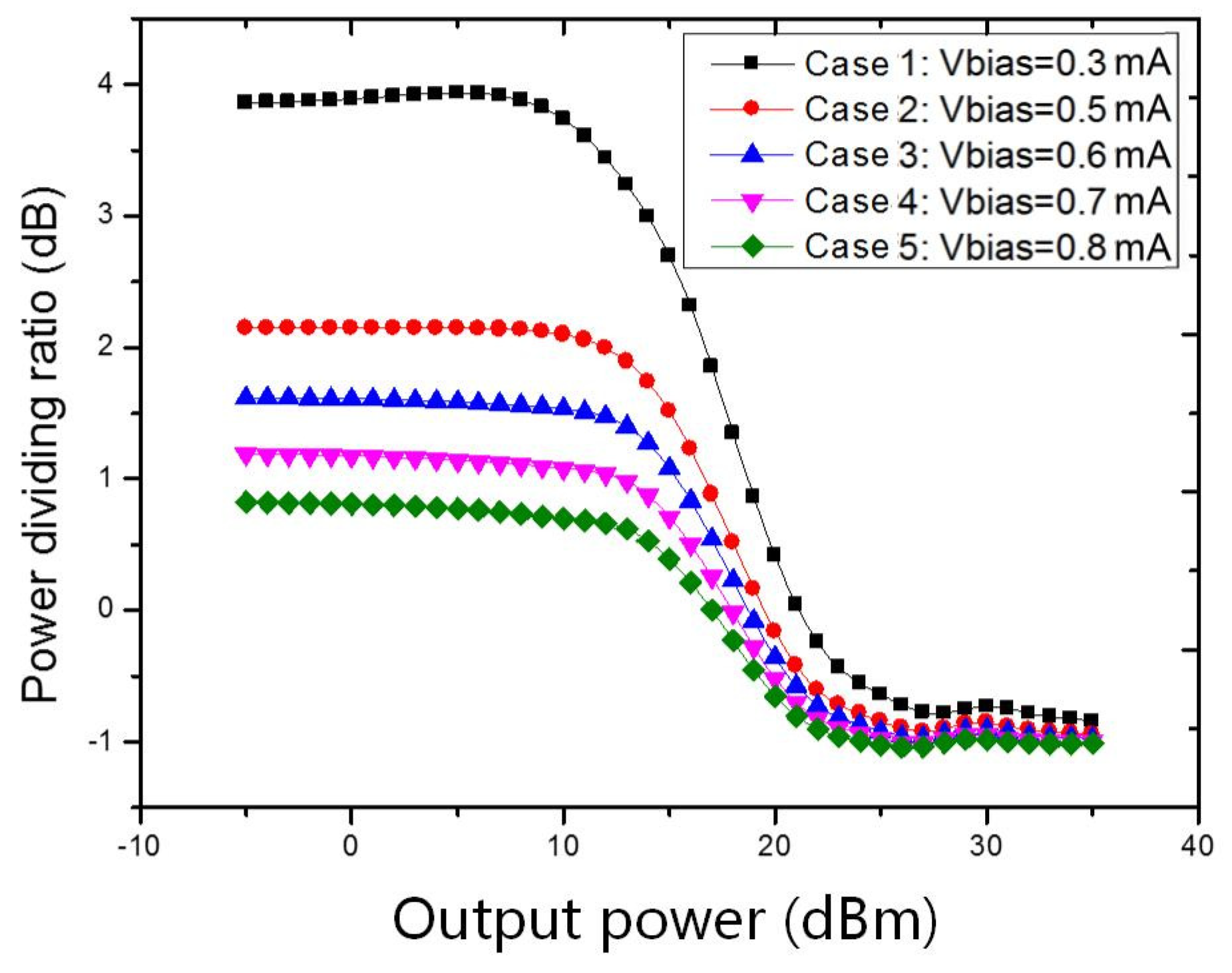
Adaptive Bias Control:
Implementing adaptive bias control strategies allows for real-time optimization of the amplifier’s performance based on the input signal characteristics [7]. By adjusting the bias points of the amplifier stages dynamically, the system can maintain an optimal balance between efficiency and linearity across varying operational conditions [8,9]. This is particularly critical in 5G applications, where the signal characteristics can change rapidly due to varying modulation schemes and channel conditions. Through the use of feedback mechanisms and digital signal processing, the amplifier can continuously monitor its performance and make necessary adjustments to the biasing, ensuring that it operates efficiently across its entire range, particularly in the back-off regions.
(3)
Three-Way Doherty Configuration:
The three-way Doherty configuration has emerged as a prominent technique for enhancing power amplifier efficiency at high output back-off levels, while introducing design trade-offs in linearity and bandwidth performance [17,18,19]. The three-way DPA configuration represents a significant advancement in efficiency performance for modern wireless systems, particularly in high PAPR applications like 4G/5G. By incorporating an additional peak amplifier branch compared to conventional two-way designs, this architecture creates three distinct efficiency peaks—typically at 0 dB, 6 dB, and 12 dB back-off points. This multi-stage load modulation enables the amplifier to maintain significantly higher efficiency across a wider power back-off range when processing complex modulated signals. However, these efficiency gains come with important trade-offs. The interaction between three amplifier paths introduces more pronounced nonlinearities, resulting in 4–6 dB worse inter-modulation distortion, requiring substantially more complex digital pre-distortion. Bandwidth performance also suffers due to phase matching challenges in the complex impedance inverter network. These characteristics make the three-way Doherty not suitable for 5G NR handset application.

2.3. Bandwidth Extension with Low Supply Voltage

(1)
Parallel-Plate Couplers:
Parallel-plate couplers represent a novel approach to achieving wideband power combining in Doherty amplifiers [10,11,12]. These couplers utilize planar configurations to achieve low phase variation and high bandwidth, addressing the limitations of traditional transmission line structures. The compact nature of parallel-plate designs also facilitates easier integration into RF front-end modules, which is essential for modern handset applications. The wideband characteristics of parallel-plate couplers enable the DPA to handle multiple frequency bands without significant performance degradation, making them particularly suitable for the diverse frequency allocations utilized in 5G technology.
(2)
Multi-Section Output Networks:
As shown in Figure 3, employing multi-section output networks is another effective strategy for extending the bandwidth of Doherty amplifiers. By cascading multiple quarter-wavelength sections or using coupled-line structures, designers can create output networks that maintain effective impedance matching across a wider frequency range [3,20]. By using this multi-section approach, the output impedance of carrier and peaking amplifier is transferred to R instead of 2R in saturation. As a result, the output power will be doubled. As shown in Figure 4, the benefits of enhanced bandwidth and performance make it a worthwhile investment in the context of achieving the operational requirements for 5G applications.
In conclusion, the key technology discussions surrounding Doherty power amplifiers for 5G applications highlight the innovations and strategies employed to overcome the inherent challenges in linearity, efficiency, and bandwidth. Through these advancements, DPAs can meet the stringent demands of modern communication systems, ensuring reliable and efficient performance in a rapidly evolving technological landscape [20,21,22].

3. Doherty Power Amplifier Circuit Design

The three-stage DPA architecture in [3] exemplifies the latest implementation, and the fundamental configuration of the linear DPA is depicted in Figure 5. Key innovations include:

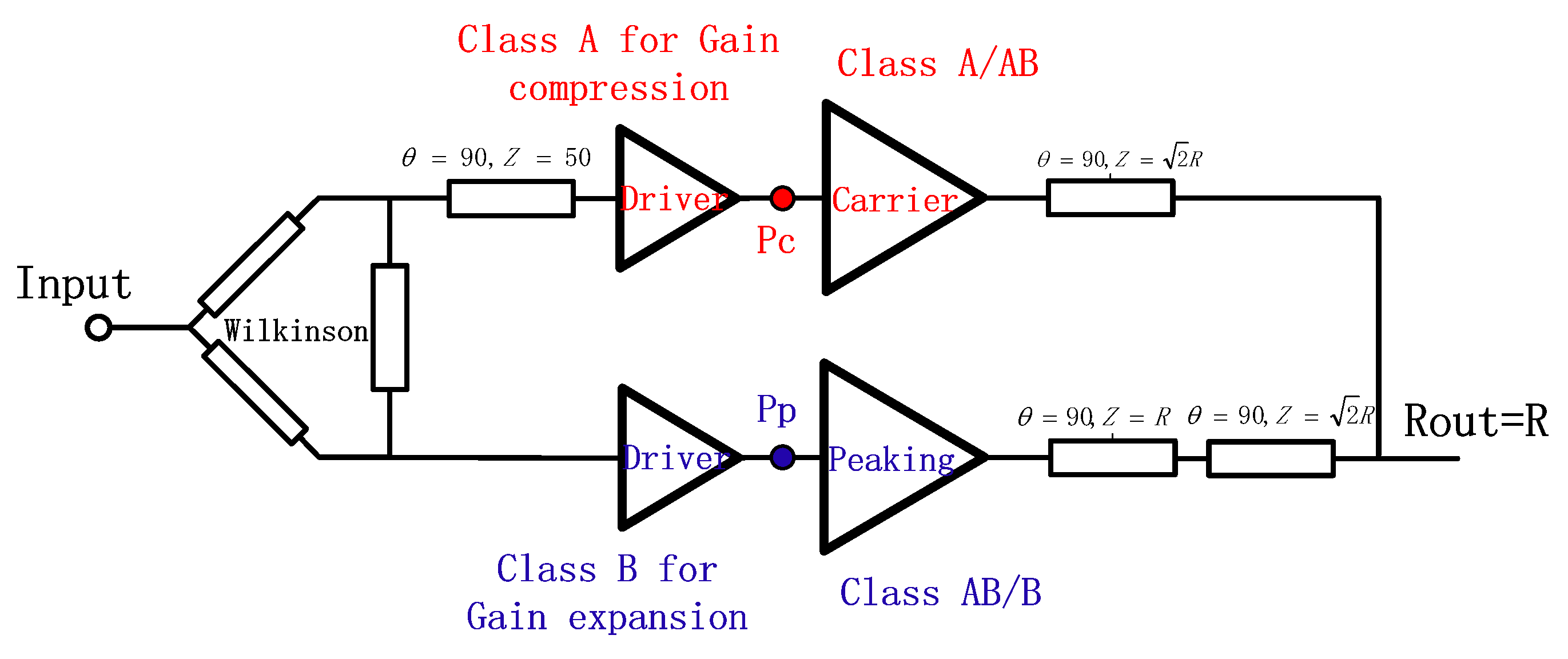
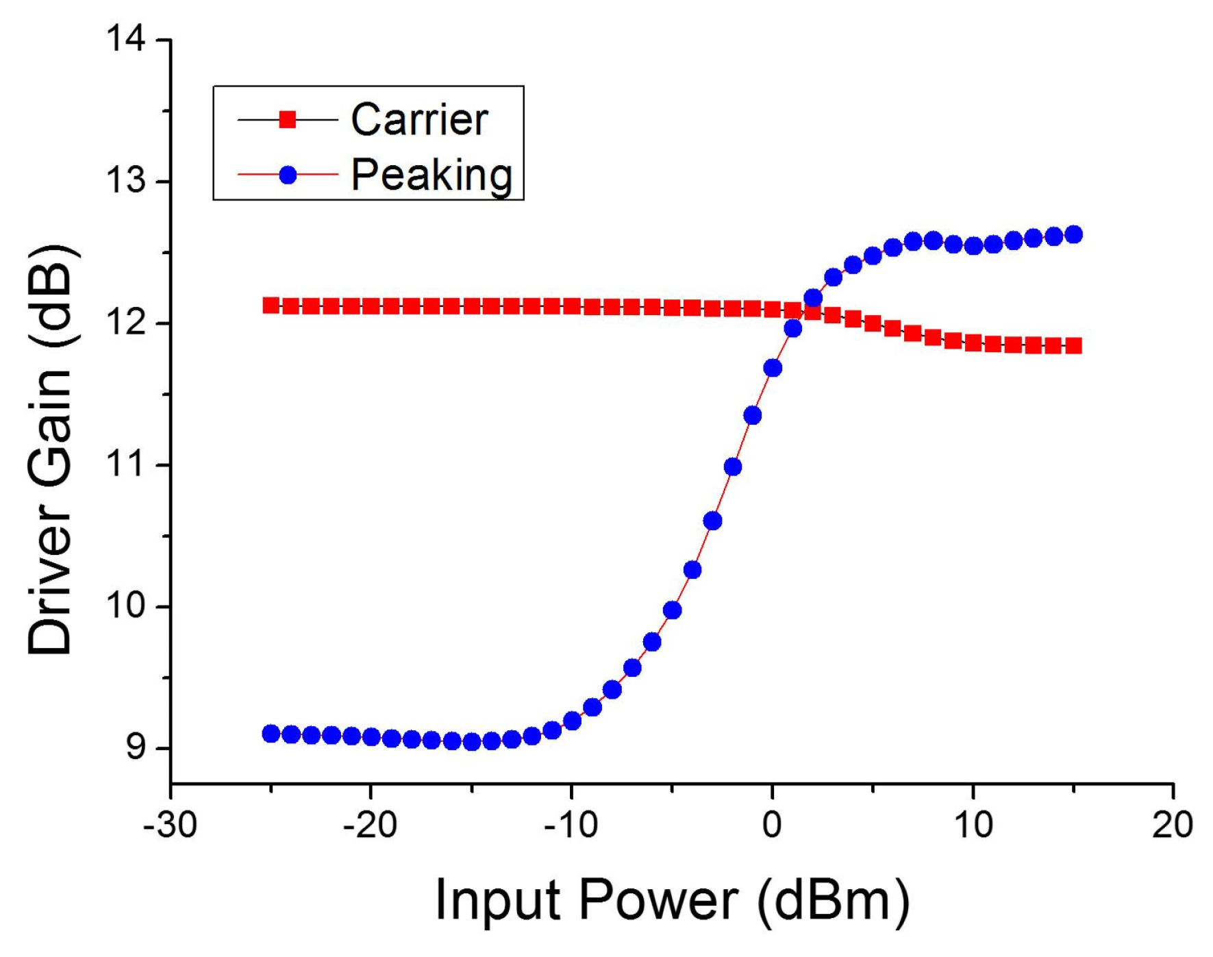
3.1. Tunable Power Allocation by Driver Amplifier

As shown in Figure 6, the driver stage biases are dynamically tuned to vary the power division ratio from 2 dB to 5 dB, optimizing the load modulation across the operating power range. This adaptive power division scheme, combined with the asymmetric carrier and peaking amplifier biases, enables a flatter AM–AM/AM–PM response and higher back-off efficiency. This technique is crucial for maintaining low ACLR performance under wide modulation bandwidths.

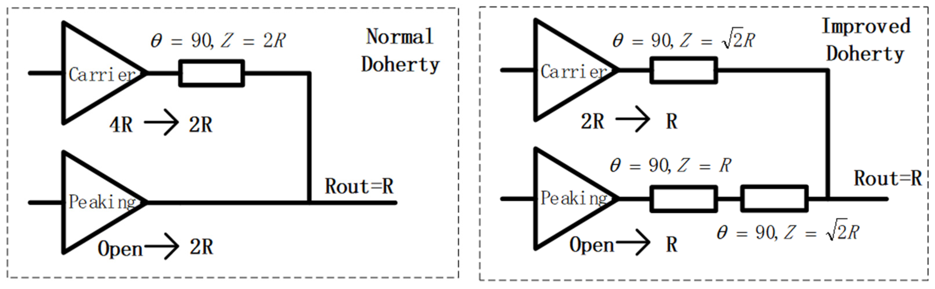
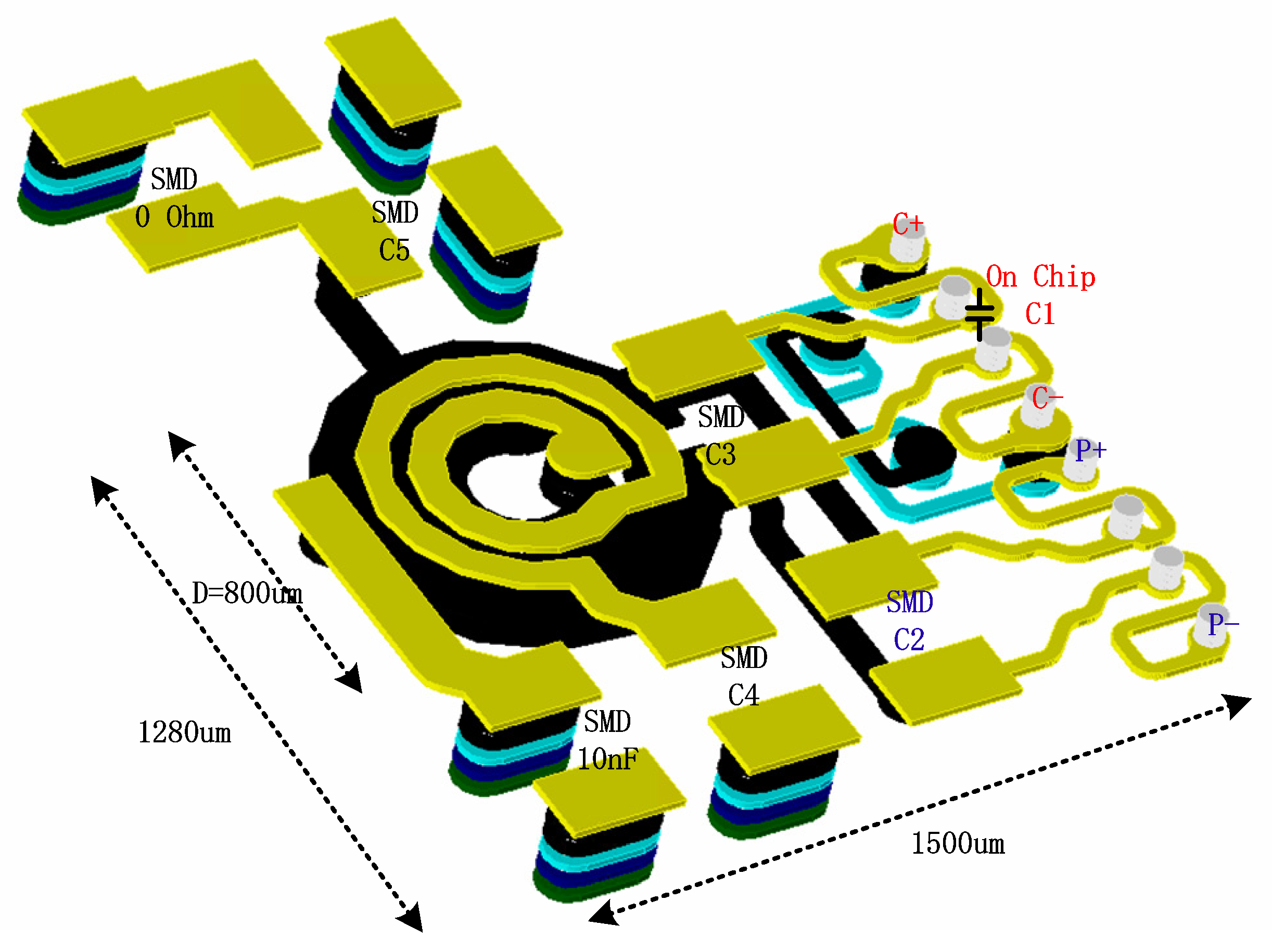
3.2. Output Network Design

The output network design of a Doherty amplifier is critical for optimizing performance, especially in terms of impedance matching. Effective impedance matching ensures maximum power transfer from the amplifier to the load, which is particularly important in high-frequency applications like 5G. One common approach is using a combination of quarter-wavelength transmission lines and lumped elements to create an impedance transformation network, as shown in Figure 7. The design can be tailored to provide optimal impedance at the operating frequency while also accommodating the varying load conditions that occur during operation. By using quarter-wavelength transmission lines network technique, the same output power can be achieved under low supply condition without decreasing the output impedance of transformer. Meanwhile, transformer-based power amplifiers offer the advantages of compact size, high impedance transformation ratio, and wide bandwidth, making them widely adopted in high-power, high-efficiency PA designs [23,24,25].
Figure 8 illustrates a three-dimensional representation of the LMN employing a six-layer laminated structure. The 1:4 turn ratio transformer was implemented using three uppermost metal layers, achieving an inductance ratio of 1:10 (Lp = 0.42 nH, Ls = 4.2 nH). This configuration features symmetrical narrow-turn windings in M1 and M3 layers electromagnetically coupled with a broader intermediate M2 layer to maximize coupling efficiency, all contained within an 800 μm diameter footprint. The laminate-exclusive Pi network inductors, fabricated using only M1 and M2 layers for optimal Q-factor, complement the design. Power supply Vcc2 connects through the transformer’s center tap with 10 nF surface-mount decoupling capacitors, requiring merely four external capacitors for simplified LMN implementation.
ANSYS HFSS 2024R1 simulations of the 3D electromagnetic model incorporating bump pillars demonstrated total losses of 0.3 dB in the carrier path, 0.6 dB in the peaking path, and 0.5 dB transformer loss across the operational bandwidth. This topology provides 0.1 dB higher loss in peaking path due to the two-segment Pi network. But it is worth if considering the other benefits. In addition, to extend the bandwidth, the quarter-wavelength transmission line can be equivalently replaced by multiple LC networks, but this will introduce significant loss. Therefore, the circuit design here needs to consider the trade-off between bandwidth and loss.

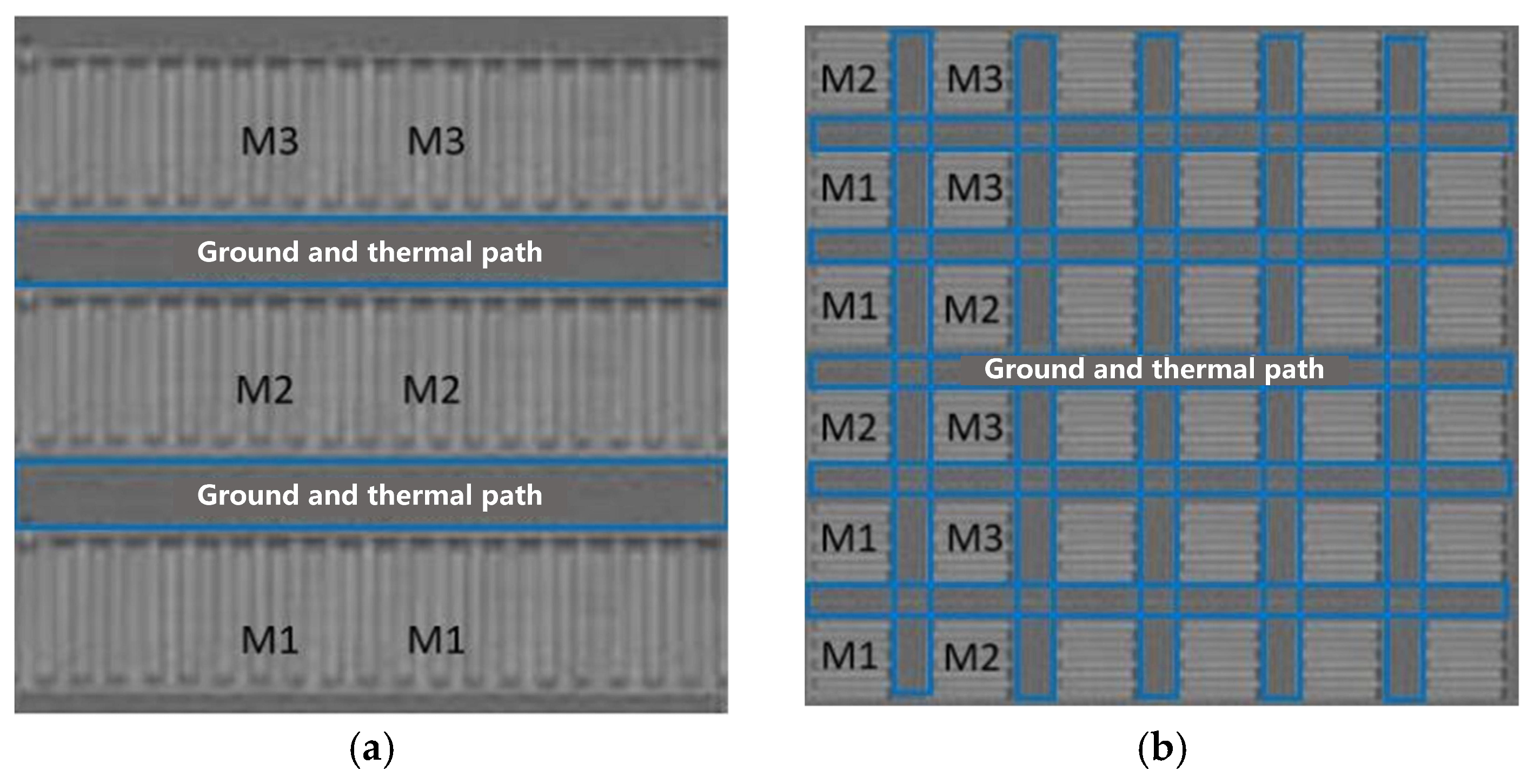
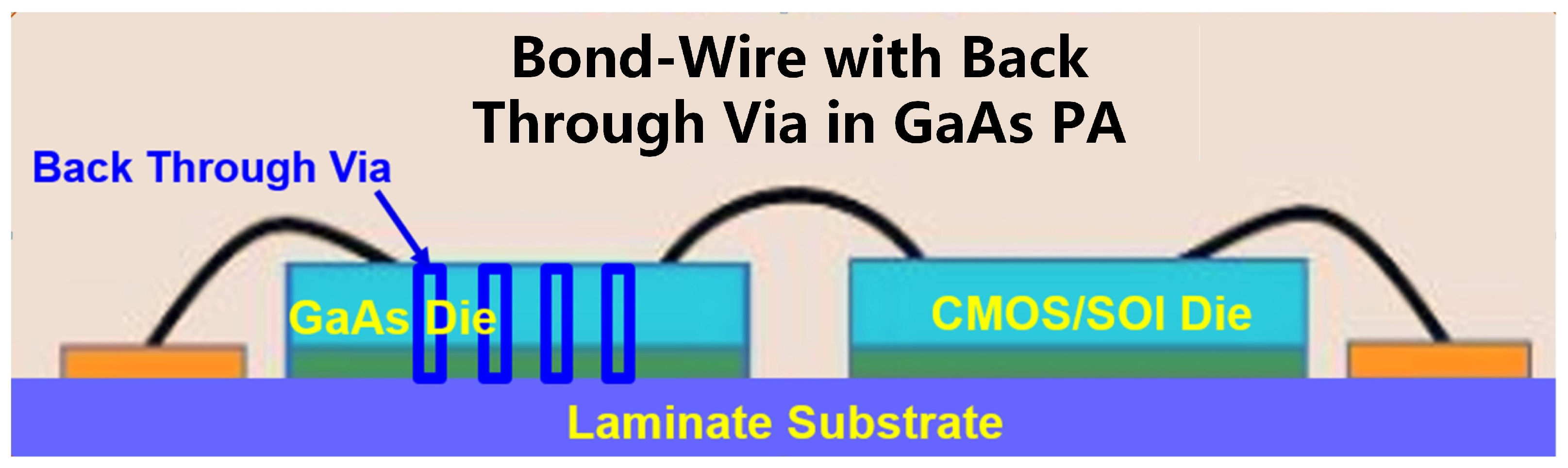
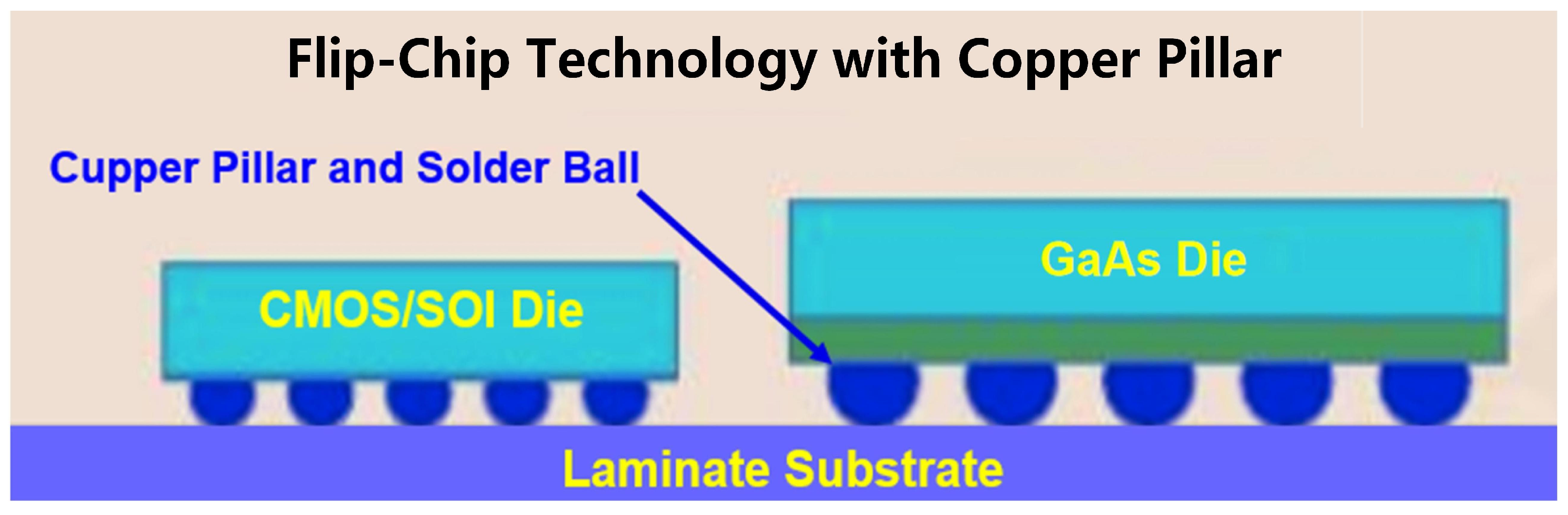
3.3. Thermal Management

(1) Chip layout–level thermal analysis:
Due to the large layout size of PA power cell core, the parasitic parameters including resistance, capacitance, and inductance between sub-cells affect the performance of the whole chip die greatly. Also, because of the high saturated power, thermal coupling between transistors brings a big thermal design challenge. In order to push the performance to the limit of transistor, the geometry of layout should be optimized to decrease the parasitic effect and thermal coupling.
Common state-of-art solutions to such thermal design challenges include increasing the size of thermal bars and improving the heat dissipation environment to avoid heat spot breakdown and adopting novel power devices [13]. In layout design, optimizing the cooling environment can be achieved by changing the spacing or length of fingers and constructing a strong ground thermal path to obtain a uniform temperature distribution of the power cells [14,15,16].
In this work, two kinds of different layout geometries in power cell are presented, as show in Figure 9a. The conventional layout shows the merits of easy connection and signal isolation between transistors, but it leads to the risk of heat spot in the layout, thus burning the transistors under certain conditions. The main concept of layout configuration in this study is the geometrical thermal isolation of power sub-cells. As illustrated in Figure 9b, the power sub-cells are divided into smaller sizes with strong ground surrounding. Although the connection of this layout structure is complex and brings more parasitic capacitance, it can be solved by careful layout and accurate parasitic extraction. As shown in Figure 10, this layout geometry shows an overwhelming advantage of average thermal distribution with lower working temperature. The thermal performance is simulated by heatwave software provide by Agilent Corporation. By distributing the power sub-cells, the maximum operating temperature of the power transistors is decreased by 25 °C when the PA is in saturated operation with a continuous wave signal.
(2) System-level thermal analysis:
Thermal analysis in package systems presents increased complexity, requiring consideration of thermal dissipation variations across different technologies and architectures, alongside reliability, cost, and manufacturing consistency factors. As illustrated in Figure 11 and Figure 12, two primary packaging technologies emerge: bond-wire and flip-chip configurations, with their thermal and characteristic comparisons detailed in Table 1. The flip-chip approach demonstrates distinct advantages, offering superior thermal dissipation performance and enhanced manufacturing consistency compared to traditional wire-bonding methods. Thermal performance is particularly important in high-power applications like 5G, where amplifiers can generate significant heat. Effective thermal management solutions, such as thermal vias and heat sinks, can be integrated within the packaging design to ensure reliable operation.

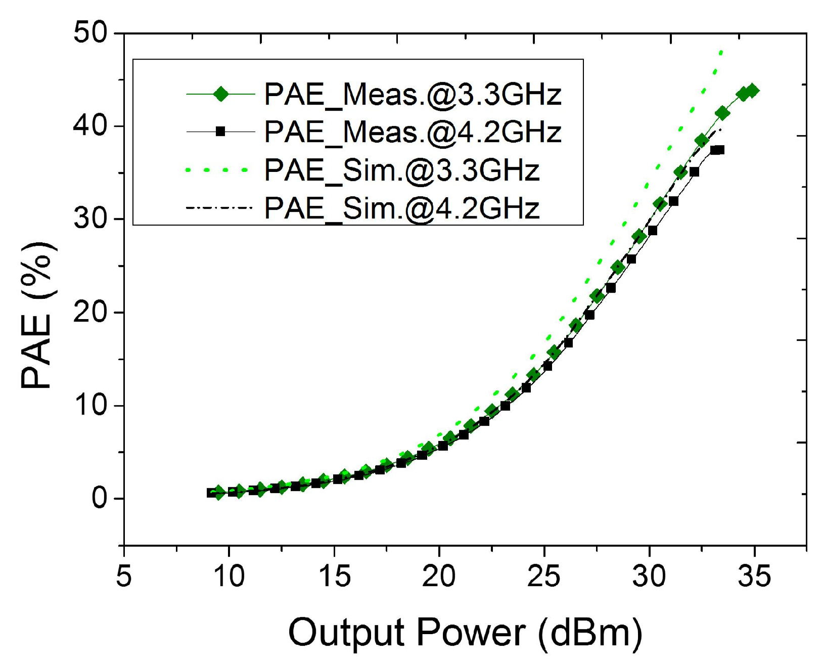
4. Implementation Results

The trend toward monolithic integration in RF front-end designs is driven by the need for compact and cost-effective solutions in 5G handsets. By integrating the DPA with other RF components, such as filters, switches, and low-noise amplifiers, manufacturers can significantly reduce the size of the overall module. Monolithic microwave integrated circuit (MMIC) technology allows for the fabrication of multiple components on a single chip, reducing inner-connect losses and improving reliability. This integration not only minimizes the physical footprint, but also enhances performance by reducing parasitic inductances and capacitances that can degrade signal integrity.
Figure 13 shows a recent photograph of the PA module [3]. The GaAs HBT PA chip, two CMOS controller chips, output transformer, and SMD components are mounted on a six-layer laminate substrate. The Doherty PA is fabricated in a GaAs HBT 2 μm two-layer metal flip-chip process with a chip area of 1.1 mm by 1.3 mm. The PA chip with output-matching circuits occupies an area of 1.3 mm by 2.5 mm on the laminate. To verify the PA module, an evaluation board is fabricated using FR-4 printed circuit board (PCB). By carefully considering the integration and packaging aspects, designers can create highly efficient and compact DPA solutions that meet the stringent requirements of 5G systems.
As shown in Figure 14, the PA module achieves a Psat of 34.8 dBm with 43% PAE at the N78 band. In the high frequency region of the N77 band, the PA module shows more than 33.4 dBm Psat with 38% PAE. The adjacent channel leakage ratio (ACLR) performance versus output power at different frequency bands is measured using a 5G NR–modulated FDD-DFTs-100MHz-QPSK signal. Figure 15a shows that this Doherty PA module achieves about 31 dBm Pout with −36 dBc ACLR at the N78 band from 3.3 to 3.75 GHz. As shown in Figure 15b, the maximum linear output power is about 30 dBm with −36 dBc ACLR1 at 4.0 and 4.2 GHz at the N77 band, respectively. At the N78 band, the proposed Doherty PA module also supports 25 dBm output power, while the EVM is less than 2%. By optimizing the bias voltage of driver amplifiers, the maximum linear output powers are 24.5 and 24 dBm (2% EVM) at 4.0 and 4.2 GHz at the N77 band, respectively.
Table 2 gives a summary of RF performances measured in this work. Compared with other works, this work shows obviously wider bandwidth, higher liner output power, and better efficiency with a smaller chip die and laminate module. To the best of the authors’ knowledge, this is the first broadband Doherty power amplifier for 5G NR handset applications with a low supply voltage of 3.4 V. The improvements in PAE, ACLR, and bandwidth demonstrate the effectiveness of the key innovations discussed in the previous sections. The PAE at 6 dB PBO increased by 5% to 10%, indicating a significant enhancement in back-off efficiency. The ACLR improvement of 3 dB showcases the advancement in linearity through IMD3 cancellation. Moreover, the fractional bandwidth expanded, thanks to the compact output combiner design and lumped-element impedance transformation.
Despite the increased circuit complexity, the chip area remains under 1.5 mm2 [4,10,25], highlighting the high level of integration achieved in recent DPA designs. The trade-off between size and performance has been carefully managed, demonstrating the maturity of the DPA technology for 5G handset front-end modules.

5. Conclusions

This comprehensive review of state-of-the-art Doherty power amplifiers for 5G handset applications has highlighted the recent advancements in linearity enhancement, back-off efficiency improvement, and broadband operation. Key innovations, including dynamic power division, IM3 cancellation, parallel-plate couplers, and compact output combiners, have enabled DPAs to achieve superior performance in terms of efficiency, linearity, and bandwidth compared to conventional designs. Furthermore, the study comprehensively investigated how optimized chip layout design and flip-chip system-level packaging implementation affect thermal dissipation and overall device performance. The trade-offs between chip area, output power, operational bandwidth, and thermal management were quantitatively investigated to guide the development of highly integrated 5G handset front-end modules.
The findings in this review provide a clear understanding of the current landscape and future directions in DPA technology for 5G NR applications. It is worth mentioning that, in addition to high Vcc operation using buck-boost DC-DC converters, low Vcc operation has been explored in the recent cellular system for low cost. This will make PA design more challenging. By addressing the critical challenges of linearity, back-off efficiency, and bandwidth, the DPA architectures presented here have demonstrated their potential to meet the stringent requirements of 5G handset PAs. The combination of advanced linearization techniques, efficient load modulation, and wideband impedance transformation has paved the way for highly integrated and energy-efficient 5G front-end solutions. As the 5G ecosystem continues to evolve, further research opportunities exist in exploring novel circuit topologies, device technologies, and system-level integration to push the boundaries of DPA performance. The review presented in this paper serves as a valuable resource for researchers, engineers, and industry professionals working on the development of cutting-edge linear 5G handset power amplifiers.

Author Contributions

Conceptualization, S.H. and H.C.; data correlation, S.H. and H.C.; writing—original draft preparation, S.H.; writing—review and editing, S.H. and H.C.; formal analysis, all authors; supervision, S.H. All authors have read and agreed to the published version of the manuscript.

Funding

This research received no external funding.

Institutional Review Board Statement

Not applicable.

Informed Consent Statement

Not applicable.

Data Availability Statement

Not applicable.

Acknowledgments

The author wish to acknowledge helpful discussions with Huan Chen.

Conflicts of Interest

Authors Shihai He and Huan Chen were employed by the company Beijing Onmicro Electronics Co., Ltd. The authors declare there is no conflict of interest for the manuscript.

References

  1. Kim, B.; Cho, Y. Design of linear Doherty power amplifier for handset application. In Proceedings of the 2016 IEEE MTT-S International Microwave Symposium (IMS), San Francisco, CA, USA, 22–27 May 2016; pp. 1–3. [Google Scholar]
  2. Cho, Y.; Kang, D.; Kim, J.; Moon, K.; Park, B.; Kim, B. Linear Doherty Power Amplifier with an Enhanced Back-Off Efficiency Mode for Handset Applications. IEEE Trans. Microw. Theory Tech. 2014, 62, 567–578. [Google Scholar] [CrossRef]
  3. Shihai, H.; Liang, J.; Linjian, X.; Meng, H.; Qian, Y. A High Efficiency and High Linearity GaAs HBT Doherty Power Amplifier for 5G NR 3.4V Application. In Proceedings of the 2024 IEEE/MTT-S International Microwave Symposium—IMS 2024, Washington, DC, USA, 16–21 June 2024; pp. 370–373. [Google Scholar] [CrossRef]
  4. Oh, H.; Choi, W.; Koo, H.; Shin, J.; Chen, Y.; Jeon, H.; Choi, Y.; Jung, H.; Hwang, J.; Yang, Y. 2.8–3.8 GHz Broadband InGaP/GaAs HBT Doherty Power Amplifier IC for 5G New Radio Handset. In Proceedings of the 2022 IEEE/MTT-S International Microwave Symposium—IMS 2022, Denver, CO, USA, 19–24 June 2022; pp. 849–852. [Google Scholar]
  5. Yu, H.; Sahlabadi, M.H.; Traore, E.; Eladwy, M.; Ma, H.; Boumaiza, S. 37–43 GHz Wide-Band Doherty Power Amplifier with Enhanced AM-PM Characteristic. In Proceedings of the 2023 IEEE/MTT-S International Microwave Symposium—IMS 2023, San Diego, CA, USA, 11–16 June 2023; pp. 935–938. [Google Scholar]
  6. Imai, S.; Okabe, H.; Tanaka, S. A Bandwidth-Optimized Transformer-Based Doherty Power Amplifier for 5G Power Class 2 Handset operation at 2.2 GHz–2.7 GHz. In Proceedings of the 2021 IEEE MTT-S International Microwave Symposium (IMS), Atlanta, GA, USA, 7–25 June 2021; pp. 791–794. [Google Scholar]
  7. He, S.; Peng, F.; Xu, L.; Meng, H.; Qian, Y. Compact High Efficiency and High Power Front-end Module for GSM/EDGE/TD-SCDMA/TD-LTE Applications in 0.13 um CMOS. In Proceedings of the 2018 IEEE Asian Solid-State Circuits Conference (A-SSCC), Tainan, Taiwan, 5–7 November 2018; pp. 289–292. [Google Scholar] [CrossRef]
  8. Uchida, Y.; He, S.; Yang, X.; Liu, Q.; Yoshimasu, T. 5-GHz band linear CMOS power amplifier IC with a novel integrated linearizer for WLAN applications. In Proceedings of the 2012 IEEE International Symposium on Radio-Frequency Integration Technology (RFIT), Singapore, 21–23 November 2012; pp. 240–242. [Google Scholar] [CrossRef]
  9. He, S.; Uchida, Y.; Yang, X.; Liu, Q.; Yoshimasu, T. 5.25 GHz linear CMOS power amplifier with a diode-connected NMOS bias circuit. In Proceedings of the 2012 International Conference on Microwave and Millimeter Wave Technology (ICMMT), Shenzhen, China, 5–8 May 2012; pp. 1–4. [Google Scholar] [CrossRef]
  10. Takenaka, K.; Noguchi, Y.; Takenouchi, Y.; Okabe, H.; Wada, T. Parallel Plate Coupler Based Doherty Power Amplifier Design for 5G NR Handset Applications. In Proceedings of the 2021 IEEE MTT-S International Microwave Symposium (IMS), Atlanta, GA, USA, 7–25 June 2021; pp. 523–526. [Google Scholar]
  11. Takenaka, K.; Noguchi, Y.; Arayashiki, S.; Wada, T. Multiband Doherty Power Amplifier Design for 5G NR Sub-6 GHz Handset Applications. In Proceedings of the 2022 Asia-Pacific Microwave Conference (APMC), Yokohama, Japan, 9 November–2 December 2022; pp. 749–751. [Google Scholar]
  12. Takenaka, K.; Sato, T.; Matsumoto, H.; Kawashima, M.; Nakajima, N. New compact Doherty power amplifier design for handset applications. In Proceedings of the 2017 IEEE Topical Conference on RF/Microwave Power Amplifiers for Radio and Wireless Applications (PAWR), Phoenix, AZ, USA, 15–18 January 2017; pp. 81–83. [Google Scholar]
  13. He, S.; Xu, L.; Meng, H. A Performance Study of Layout in 0.13 um CMOS Power Amplifier for 4G Mobile Front-End Module. In Proceedings of the 2024 IEEE International Symposium on Radio-Frequency Integration Technology (RFIT), Chengdu, China, 28–30 August 2024; pp. 1–3. [Google Scholar]
  14. Srinivasan, P.; Gonzalez, O.H.; Restrepo, O.D.; Lestage, J.; Syed, S.; Taylor, W.; Bandyopadhyay, A.; Gall, M.; Ludvik, S. Thermal Considerations on RF Reliability and Aging in SOI CMOS Based Power Amplifiers. In Proceedings of the 2024 IEEE International Reliability Physics Symposium (IRPS), Grapevine, TX, USA, 14–18 April 2024; pp. 1–6. [Google Scholar] [CrossRef]
  15. Alluri, S.; Jayamon, J.; Hanafi, B.; Asbeck, P. Simulation Technique for Thermal Resistance in CMOS-SOI Power Amplifier Integrated Circuits. In Proceedings of the 2020 IEEE Topical Conference on RF/Microwave Power Amplifiers for Radio and Wireless Applications (PAWR), San Antonio, TX, USA, 26–29 January 2020; pp. 9–11. [Google Scholar] [CrossRef]
  16. Choi, S.; Peake, G.M.; Keeler, G.A.; Geib, K.M.; Briggs, R.D.; Beechem, T.E.; Shaffer, R.A.; Clevenger, J.; Patrizi, G.A.; Klem, J.F.; et al. Thermal Design and Characterization of Heterogeneously Integrated InGaP/GaAs HBTs. IEEE Trans. Compon. Packag. Manuf. Technol. 2016, 6, 740–748. [Google Scholar] [CrossRef]
  17. Pelk, M.J.; Neo, W.C.E.; Gajadharsing, J.R.; Pengelly, R.S.; de Vreede, L.C.N. A High-Efficiency 100-W GaN Three-Way Doherty Amplifier for Base-Station Applications. IEEE Trans. Microw. Theory Tech. 2008, 56, 1582–1591. [Google Scholar] [CrossRef]
  18. Zhou, H.; Perez-Cisneros, J.-R.; Hesami, S.; Buisman, K.; Fager, C. A Generic Theory for Design of Efficient Three-Stage Doherty Power Amplifiers. IEEE Trans. Microw. Theory Tech. 2022, 70, 1242–1253. [Google Scholar] [CrossRef]
  19. Kim, I.; Moon, J.; Jee, S.; Kim, B. Optimized Design of a Highly Efficient Three-Stage Doherty PA Using Gate Adaptation. IEEE Trans. Microw. Theory Tech. 2010, 58, 2562–2574. [Google Scholar] [CrossRef]
  20. Musolff, C.; Kamper, M.; Abou-Chahine, Z.; Fischer, G. Linear and Efficient Doherty PA Revisited. IEEE Microw. Mag. 2014, 15, 73–79. [Google Scholar] [CrossRef]
  21. Cho, Y.; Kang, D.; Moon, K.; Jeong, D.; Kim, B. A Handy Dandy Doherty PA: A Linear Doherty Power Amplifier for Mobile Handset Application. IEEE Microw. Mag. 2017, 18, 110–124. [Google Scholar] [CrossRef]
  22. Courty, A.; Quindroit, C.; Bouny, J.-J.; Ferris, P.; Rochas, P.; Moronval, X. A 3.7–4.2GHz MMIC Doherty Power Amplifier Linearized over 500MHz Instantaneous Bandwidth. In Proceedings of the 2023 IEEE Topical Conference on RF/Microwave Power Amplifiers for Radio and Wireless Applications, Las Vegas, NV, USA, 22–25 January 2023; pp. 29–31. [Google Scholar] [CrossRef]
  23. Cho, Y.; Moon, K.; Park, B.; Kim, J.; Kim, B. Voltage-Combined CMOS Doherty Power Amplifier Based on Transformer. IEEE Trans. Microw. Theory Tech. 2016, 64, 3612–3622. [Google Scholar] [CrossRef]
  24. Park, H.C.; Kim, S.; Lee, J.; Jung, J.; Baek, S.; Kim, T.; Kang, D.; Minn, D.; Yang, S.G. Single Transformer-Based Compact Doherty Power Amplifiers for 5G RF Phased-Array ICs. IEEE J. Solid-State Circuits 2022, 57, 1267–1279. [Google Scholar] [CrossRef]
  25. Bo, S.F.; Ou, J.-H.; Peng, Y.J.; Xuan, K.; Xu, J.-X.; Zhang, X.Y. Broadband GaAs HBT Doherty Power Amplifier for 5G NR Mobile Handset. IEEE Trans. Circuits Syst. II Express Briefs 2024, 71, 527–531. [Google Scholar] [CrossRef]
Figure 1. Simulated IM3 and fundamental signal vs. input power: (a,b) at lower frequency; and (c,d) at higher frequency.
Chips 04 00020 g001aChips 04 00020 g001b
Figure 2. Simulated PDRs vs. input power with different bias currents.
Chips 04 00020 g002
Figure 3. Simplified output impedance transform diagram.
Chips 04 00020 g003
Figure 4. Load modulation: (a) simplified output impedance transform diagram; (b) simulation results.
Chips 04 00020 g004
Figure 5. Architecture diagram of the typical Doherty power amplifier module.
Chips 04 00020 g005
Figure 6. Simulated driver gain vs. input power.
Chips 04 00020 g006
Figure 7. Output matching circuit of the Doherty power amplifier.
Chips 04 00020 g007
Figure 8. The implementation of output matching circuits.
Chips 04 00020 g008
Figure 9. Comparison of different power cell layout geometries. (a) Conventional structure and (b) distribution structure.
Chips 04 00020 g009
Figure 10. Thermal simulation results of the power cells. (a) Conventional structure and (b) distribution structure.
Chips 04 00020 g010
Figure 11. Bond-wire technology in chips.
Chips 04 00020 g011
Figure 12. Flip-chip technology in chips.
Chips 04 00020 g012
Figure 13. Photograph of the implemented Doherty PA.
Chips 04 00020 g013
Figure 14. Measured PAE versus output power from 3.3 to 4.2 GHz using a CW signal.
Chips 04 00020 g014
Figure 15. Measured ACPR versus output power: (a) ACLR at the N78 band; (b) ACLR at the N77 band.
Chips 04 00020 g015
Table 1. Comparison of the bond-wire and flip-chip technologies.
Bond-Wire in GaAsFlip-Chip in GaAs
Advantages
1.
Thermal resistance
The GaAs substrate should be thinner for better heat dissipation. But to be thinner, it will be more fragile.
1.
Low cost and easy connection
No expensive gold layer, but normal copper bumps.
2.
High consistency of matching
All the inductors realized on laminate show better consistency.
3.
Low thermal resistance
Strong ground connection through numerous solid cupper pillars.
4.
Low parasitic inductance
Easy to achieve high performance.
Disadvantages
1.
High cost and high complexity
Golden bond wires connect with components on the laminate substrate through golden pads.
2.
Bad consistency of bond wires
The variation of height of bond wires may result in deviation of performance in massive production.
1.
Limited thermal cycling reliability
Flip-chip interconnects experience high thermal stress due to coefficient of thermal expansion (CTE) mismatch between the chip and substrate, potentially leading to solder joint fatigue failures.
Table 2. Comparison of the proposed PA with recently reported PA.
Ref.[10] 2021 IMS[4] 2022 IMS[21] 2023 TCSII[3] 2024 IMS
Supply Voltage (V)3.84.55 V3.4 V
Frequency (GHz)3.35–4.152.8–3.83.3–4.23.35–4.15
PA ProcessGaAs HBT (Flip-chip)GaAs HBT (Flip-chip)GaAs HBT M3 (Bond-wire)GaAs HBT M2 (Flip-chip)
PA Die Area (mm2)1.1 × 1.11.5 × 11.34 × 1.441.1 × 1.3
Module Area (mm2)3.5 × 2.5 *, Laminate2.1 × 1.8, Laminate1.69 × 3.85, Laminate1.3 × 2.5, Laminate
CW Psat (dBm)--3633.4–34.8
CW PAE (%) @Sat.-32.2–47.339–4438–43
CW Gain33–36 *31.9–38.325.8–27.226.2–28.1
NR Pout (dBm)27.826–27.83030–31
NR PAE (%) 35–4222–30.626.2–30.331–34
NR ACPR (dBc)−35−33−32.1−36
Using DPDYesNONONO
StructureSingle-end DohertyDifferential DohertyQuadrature + single-differential DohertyWilkinson + differential Doherty
*: Graphically estimated.
Disclaimer/Publisher’s Note: The statements, opinions and data contained in all publications are solely those of the individual author(s) and contributor(s) and not of MDPI and/or the editor(s). MDPI and/or the editor(s) disclaim responsibility for any injury to people or property resulting from any ideas, methods, instructions or products referred to in the content.

