Abstract
Modern computer applications have become highly data-intensive, giving rise to an increase in data traffic between the processor and memory units. Computing-in-Memory (CiM) has shown great promise as a solution to this aptly named von Neumann bottleneck problem by enabling computation within the memory unit and thus reducing data traffic. Many simulation tools in the literature have been proposed to enable the design space exploration (DSE) of these novel computer architectures as researchers are in need of these tools to test their designs prior to fabrication. This paper presents a collection of classical nonvolatile memory (NVM) and CiM simulation tools to showcase their capabilities, as presented in their respective analyses. We provide an in-depth overview of DSE, emerging NVM device technologies, and popular CiM architectures. We organize the simulation tools by design-level scopes with respect to their focus on the devices, circuits, architectures, systems/algorithms, and applications they support. We conclude this work by identifying the gaps within the simulation space.
1. Introduction
With the rise of Deep Neural Networks (DNNs) in recent years, there is a growing demand for high-speed architectures that can process large amounts of data quickly and efficiently [1,2,3]. Computer architects are tasked with providing as much computing power in as little space as possible to meet these demands. Complementary metal-oxide-semiconductor (CMOS) technologies have significantly evolved over the past few decades, enabling the creation of smaller devices that are employed in the development of high-performance computers.
However, traditional computer architectures remain processor-centric. Based on the von Neumann design, Central Processing Units (CPUs) require multiple clock cycles to load operands into registers, perform computations in the Arithmetic Logic Unit (ALU), and store the results back into memory. Although this approach was sufficient in the past—when data storage and processing were smaller in scale and consumed less power—it currently struggles to meet modern demands. As CMOS technology enables shrinking process nodes and nanoscopic transistors [4], data storage capacities have expanded dramatically, and efficient parallelization across numerous processing cores has become essential. The so-called von Neumann bottleneck restricts parallelization, forcing CPUs to stall computation to manage data transfers, resulting in significant latency and power consumption [5]. To address these growing challenges, researchers are exploring alternative architectural designs.
Computing-in-Memory (CiM), also known as Processing-In-Memory (PIM), is an emerging architectural paradigm that aims to solve the latency and energy consumption overheads associated with intensive data traffic between the memory and processor [5]. In contrast to separating data processing and storage, CiM enables computation within the memory unit. By providing the memory unit with a means of performing computation, a designer can exploit the parallel nature of the memory unit and perform bulk computations in situ, freeing up the CPU for other tasks. This reduces the total volume of data movement as there is less need to transfer data from the CPU and the memory.
The emergence of CiM has led to the proposal of several architectures that hasten a variety of calculations and operations. For example, RowClone [6] enables the copying and initialization of Dynamic Random Access Memory (DRAM) rows by exploiting the existing row buffer. Ambit [7] expands on RowClone by utilizing it to perform bit-wise AND, OR, and NOT operations on DRAM rows. LISA [8] accelerates data transfer by improving subarray connectivity. Pinatubo [9] exploits the resistive properties of emerging nonvolatile memory (NVM) technologies to accelerate bulk bit-wise operations. ISAAC [10] uses analog arithmetic to accelerate DNN and Convolutional Neural Network (CNN) calculations. RAELLA [11] accelerates DNN inference using resistive RAM (abbreviated as RRAM or ReRAM) crossbar arrays and low-resolution analog-to-digital converters (ADCs). FlexiPIM [12] proposes an NVM crossbar design to enhance operations used by DNNs. MAGIC [13] and IMPLY [14] enable Boolean logic evaluation in the crossbar by exploiting the properties of RRAM cells. MRIMA [15] accelerates bit-wise adding and convolving for CNN applications, and data encryption for use in the advanced encryption standard (AES) algorithm.
Although the research community has shown significant interest in this solution, as demonstrated by numerous design proposals, several roadblocks still prevent CiM from being adopted on a large scale. One of the major hurdles is the high cost associated with the fabrication and testing of CiM architectures. Given that many CiM designs utilize NVMs, the immaturity of these technologies also presents significant challenges. Furthermore, designers face a vast architectural design space that spans several levels of granularity, where the choices made at each level can affect the performance of the overall system. For example, the choice to use an NVM device over a classical memory device ultimately affects the circuit configuration options that are available for that device. As a result, CiM designs require extensive testing and validation before fabrication.
Previous surveys have provided analyses on CiM and memory simulators. Onur Mutlu et al. [5] provide a broad overview of CiM and cover details on popular architectures. Zhong Sun et al. [16] examine a large collection of CiM schemes at the circuit level. Ayaz Akram et al. [17] discuss simulation techniques and tools for standard designs but do not cover tools that are tailored toward CiM designs and NVM device technologies. Inseong Hwang et al. [18] provide a broad collection of simulation tools in their analysis but only briefly discuss three CiM simulation tools. Felix Staudigl et al. [19] improve on this by including an analysis of ten CiM simulation tools, but they only focus on tools with use cases related to neural network (NN) applications. None of these works consider the broad simulation space of CiM designs across many different applications.
This paper presents a collection of simulation tools [20,21,22,23,24,25,26,27,28,29,30,31,32,33,34,35,36] for NVM devices and CiM designs to showcase their capabilities and limitations. A total of twenty simulation tools are analyzed to evaluate the flexibility they offer designers in specifying and mapping their designs without requiring further modifications. We examine their capabilities across a vast design space and provide a comprehensive overview of the simulator environment as it currently stands. In this field, much more work is needed to grant circuit designers and architects the ability to create, test, and compare their designs quickly, fairly, and accurately.
The paper is organized as follows. Section 2 provides the background of the design process for CiM architectures, which includes the options of memory technology and peripheral circuits that designers can choose from. In Section 3, we discuss our methodology for showcasing CiM simulators and what designers are looking for in a robust simulator. In Section 4, we present several CiM simulators from the recent literature. In Section 5, we compare the capabilities and limitations of the selected CiM simulation frameworks. In Section 6, we discuss the future work needed in CiM simulation tools to encapsulate a wider variety of designs and use case scenarios.
2. Design Space Exploration (DSE)
The design of any accelerator architecture consists of building blocks at different hierarchical levels. Figure 1 summarizes the design components that make up each level. Each level presents a list of options for architects to consider in their designs, so there are many different possible architectures to choose from. Architects narrow down the choices by choosing a specific application, deciding which metrics to optimize (e.g., area, latency, power consumption, etc.), and limiting exploration to lower levels. The process of deciding which combination of algorithms, architectures, circuits, and devices best meets their chosen application is known as design space exploration (DSE).

Figure 1.
The design space levels for accelerator architectures. Architects have many options to consider for their designs at each of these levels.
The existing simulation tools for CiM and NVMs may prioritize one of these levels, or may span several levels simultaneously. These tools provide support for the simulation of specific device technologies, circuits, architectures, systems, and end-user applications. Simulators provide insight into the performance and overall quality of the design by measuring key metrics, and designers can choose which metrics they wish to optimize. Table 1 outlines the metrics of importance and which design levels focus on these metrics. We define the metrics as follows:

Table 1.
Design metric focus at each design level.
- Latency measures the system’s speed in producing an output after input signals change.
- Throughput is a measure of how much data are fully processed within a unit of time.
- Area refers to the physical space the system occupies.
- Power consumption is a measure of how much power the system needs to operate.
- Endurance measures how many cycles a device can be programmed before it becomes inoperable.
- Data retention refers to how long the system can maintain its memory state.
- CMOS Process Compatibility determines whether current fabrication processes can create these devices.
We examine the design choices for optimizations at each level in detail to illustrate the broad design space of CiM architectures.
2.1. Device Level
The device level consists of memory cell technologies that serve as the fundamental building blocks in many CiM designs. The selection of a memory cell technology drives the higher-level architectural decisions since the capabilities of the memory cell provide enhancements in some designs and limitations in others. The designer has to make a prediction on which technology will provide the desired performance metrics for their application while acknowledging the trade-offs required to utilize that technology.
In CiM, it is possible to construct designs that utilize classical memory technologies, such as static RAM (SRAM) [37], DRAM [38], and Flash [39]. Alternatively, some designs exploit NVM devices, such as RRAM [40,41], magnetoresistive RAM (MRAM) [42], phase change memory (PCM) [43], and ferroelectric field effect transistors (FeFETs) [44]. These emerging devices have properties that enable them to have different states. Should a designer choose to utilize NVM devices in their designs, they will need to consider the ratio between these states for each device. If this ratio is too small, such that sense amplifiers and other peripheral circuits cannot distinguish between states, then computation becomes infeasible.
It is possible to construct a memory cell capable of storing more than one bit in a multi-level cell (MLC) configuration. This is achieved by utilizing either a resistive memory capable of differentiating between multiple states or using two or more memory devices per cell. Thus, designers have several device options to choose from, where different devices can drastically affect performance metrics. Figure 2 describes the structure and operation of some of these NVM devices. We discuss these in detail as many CiM architectures exploit their properties.
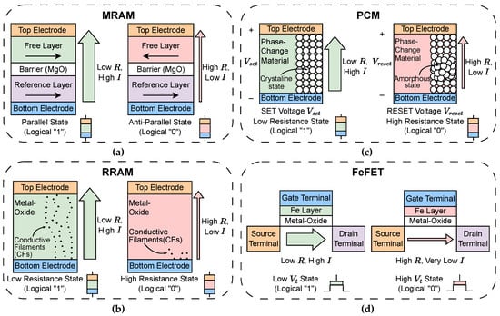
Figure 2.
Structure and operation of emerging nonvolatile memory (NVM) devices. Logical “0” is represented whenever the device has high resistance across terminals (light red), and logical “1” is represented when the device has low resistance across terminals (light green). The presented devices are (a) MRAM, (b) RRAM, (c) PCM, and (d) FeFET.
2.1.1. Magnetoresistive Random Access Memory (MRAM)
Fundamentally, the cell of an MRAM device (Figure 2a) consists of two magnetic layers that are separated by an insulating layer known as the “tunneling barrier” in a metal–insulator–metal (MIM) stack [42]. This stack as a whole is called a magnetic tunnel junction (MTJ). The bottom electrode is connected to the ferromagnetic reference layer, whose magnetic polarity remains fixed. The top electrode is connected to the ferromagnetic free layer (also known as the recording/storage layer), whose magnetic polarity can change. The width of the dielectric tunneling barrier plays a significant role in how the MTJ changes resistance, where a small width enables the MTJ to become a variable resistor, known as a memristor. In the parallel state, both the reference layer and the free layer are magnetically oriented in the same direction. Consequently, more electrons can tunnel through the barrier, resulting in high current I and low resistance R. In the antiparallel state, the reference layer and the free layer are magnetically oriented in opposite directions. As a result, fewer electrons can tunnel through the barrier, resulting in low current and high resistance.
To perform a write, the device employs a method that allows switching between parallel and antiparallel states. Each switching method provides classification for a family of MRAM cell technologies, such as toggle MRAM, spin–transfer torque MRAM (STT-MRAM), and spin–orbit torque MRAM (SOT-MRAM). To perform a read, current must be passed through the cell, and the resistance between the reference layer and the free layer must be evaluated. The most popular configuration to accomplish this tethers one select transistor between the top electrode and the reference layer of each cell, creating a 1T-1MTJ cell. When the transistor is enabled, it allows current to flow through the cell, which generates a readable resistance value.
MRAM technology shows much promise as an emerging NVM device since it consumes little power, has fast read and write operations, and is compatible with the CMOS process. However, the device is susceptible to resistance variation and can be difficult to downscale to ideal transistor sizes.
2.1.2. Resistive Random Access Memory (RRAM)
RRAM (Figure 2b) is constructed in a similar way to MRAM but instead measures resistance based on different interactions between its layers. This MIM device is constructed with two electrodes and a metal-oxide layer in between [40]. When voltage is applied across an RRAM cell, the generated electric field encourages the formation or destruction of conductive filaments (CFs) through the oxide layer, which changes the resistance between the electrodes. When the filaments are present, they form a “wire” through which electrons can easily flow. The cell would then be in a low-resistance state (LRS). When the filaments are destroyed, they do not bridge the electrodes, and electrons cannot pass through the oxide layer. The cell would be in a high-resistance state (HRS).
As with MRAM, the selection and width of the materials used to construct these cells play a crucial role in their performance. Thicker oxide layers require a higher programming voltage to be applied across the cell, while a thinner layer causes currents to leak through the cell [41]. Overall, the device has better scaling capabilities with respect to MRAM but suffers from high leakage currents that waste power [45]. Additionally, while RRAM is also compatible with CMOS processes, the set and reset voltages of each cell have significant variance. Consequently, cells that are fabricated together in the same array may have different read and write voltages.
2.1.3. Phase Change Memory (PCM)
As with the other resistance-based memories discussed, PCM (Figure 2c) uses another property of its materials to achieve high and low resistive states. A cell of PCM contains a phase change material, which can exist in either an amorphous (high resistance) state or a crystalline (low resistance) state [43]. The choice in phase change material within the cell will ultimately determine its set/reset time, its crystallization temperature (i.e., the lower temperature that causes the material to enter its crystalline state), and its melting temperature (i.e., the higher temperature that causes the material to enter its amorphous state).
By adjusting the voltage, the cell experiences temperature changes that allow it to be set and reset. At lower voltages, the state of the device does not change, so quick reads can be performed by measuring the resistance across the cell at low voltage. Resetting the cell’s value also occurs rather swiftly as the crystalline state melts rapidly when the cell reaches its melting temperature. Unfortunately, the set speed is much slower as it takes longer for the crystals to form at the crystalline temperature. Additionally, with the device’s functionality dependent on high temperature, it is difficult to fabricate and downscale PCM devices to ideal sizes.
2.1.4. Ferroelectric Field Effect Transistor (FeFET)
The FeFET device (Figure 2d) is built upon the classical metal-oxide-semiconductor field-effect transistor (MOSFET), which utilizes a three-terminal structure. In an MOSFET, the voltage applied at the gate terminal controls conduction between the source and drain terminals. The FeFET device includes an added ferroelectric oxide layer to the MOSFET stack [44]. This new layer adjusts the voltage threshold of the MOSFET, which is the required voltage needed to be applied at the gate terminal in order to enable conduction. When the voltage threshold is low, it becomes easier to enable the device with lower voltages. When the voltage threshold is high, a higher voltage at the gate is required to enable the device. Consequently, if a read voltage applied at the gate is chosen to be between the minimum and maximum values of the device, the low state would be conducting (representing logical “1”), while the high state would not be conducting (representing logical “0”).
Applying a strong voltage at the gate terminal (determined by the materials used to construct the device) results in a change in . To sense whether the device is in a high or low state, the current across the cell from the source terminal to the drain terminal is evaluated by peripheral circuitry. As a result, the total amount of power consumption required to operate the device is reduced in comparison to devices like RRAM. These devices have also been shown to exhibit high retention; however, challenges with endurance still remain [46].
2.2. Circuit Level
The circuit level consists of the collection of memory cells, supporting peripheral circuitry (e.g., ADCs, sense amplifiers (SAs), etc.), and interconnections between them, which together form a processing element (PE). The PE usually represents one complete computational array with controllers that drive the operations enabled by the circuit design. PEs are sometimes referred to as subarrays or by more specific names, depending on the hierarchy defined by the architecture and the circuit technology. There are many different CiM circuit designs, some of which utilize a mixture of NVM technology and standard transistors to form the cells of their arrays. An in-depth review of these strategies can be found in [16].
Many tools for architects are available that encapsulate simulation at the device level and circuit level. SPICE [47] and CACTI [48] are tools that have been utilized for years to model classical memory hierarchies and cache performance. To include the novel NVM devices and CiM PEs, researchers must either devise new device models and modify the simulator to support their circuit design [49], or construct new simulators entirely to meet their needs, which is the case with NVSim [20] and NVMain 2.0 [21].
2.2.1. Crossbar/Synaptic Array
A crossbar array, also known as a synaptic array, is a collection of cells arranged to form a grid of M rows and N columns. The rows are typically connected to a shared word-line (), enabling the ability to activate or deactivate cells in a row-wise manner [50]. Figure 3 describes the structures of various well-known CiM crossbar arrays. In Figure 3a, memory cells are composed of 1-resistor (1R), where s connect the top electrodes in rows and bit-lines (s) connect the bottom electrodes in columns. While this design is simple, it suffers from leakage current flowing from unselected cells [51]. To address this issue, 1-transistor–1-resistor (1T1R) and 2-transistor–2-resistor (2T2R) cells have been proposed [52,53]. In the 1T1R array (Figure 3b), the transistor acts as a selector to allow access to that cell while also mitigating any unwanted currents from leaking down the sense-lines (s). In the 2T2R array (Figure 3c), the two access transistors share the , and the second resistor—opposite in polarity to the first resistor—is tethered to a complementary bit-line, denoted . The 1FeFET crossbar array (Figure 3d) shares similarity to the 1T1R structure, with the exception that the nonvolatile element is intrinsic to the FeFET device itself.
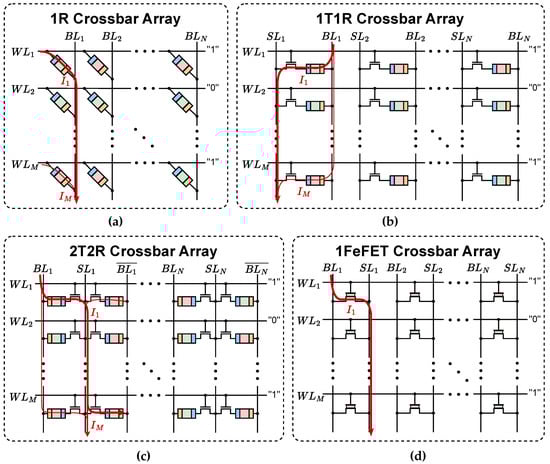
Figure 3.
The array structures of well-known CiM crossbars. Devices in light green are in a LRS while devices in light red are in a HRS. (a) A 1R crossbar array, where the voltage on the and the resistance of the device produce a current (dark red) along the , accumulating at the bottom to form a sum of products. (b) a 1T1R crossbar array, where a select transistor and an are added to provide more control over the selection of cells and to reduce leakage current. (c) a 2T2R crossbar array, where the select transistors share an and a complementary bit-line is added to enable complementary storage of bits. (d) A 1FeFET crossbar array, where the state of the device and the voltage of the determine whether or not current flows through it to the , representing another sum of products down the .
Particularly for memristive devices (i.e., those that can hold a continuous range of resistance values), these structures are capable of performing multiplication in the analog domain. By Ohm’s Law, the current across a resistor is a function of its resistance and the voltage applied to it, such that . By applying consistent voltages across s, the resistance of the cell ultimately determines the amount of current that flows through it. In 1R crossbars, current flows from the and accumulates at the bottom of the by Kirchhoff’s Current Law. In 1T1R crossbars, a voltage applied on the drives current from the to accumulate at the bottom of the . In 2T2R crossbars, the is driven by a higher voltage, and its complement is driven by a lower voltage, effectively creating a ”positive” and “negative” component of each cell, respectively. The states of the two resistors in each cell are complementary such that one is programmed to an HRS while the other is programmed to an LRS. In this manner, by sharing the , cells can add or subtract to the current accumulated at the bottom of the line. In 1FeFET crossbars, current flows from the and accumulates at the , where the acts to either enable or disable the whole row. In any case, a column line stores the sum of currents, achieving a multiply–accumulate (MAC) operation. To convert the result into the digital domain, an ADC is used as the current-sensing peripheral circuit to obtain a digital output; however, these circuits require a significant amount of power to operate.
An alternative use case for crossbar arrays is the evaluation of Boolean expressions. In this manner, the device is programmed to have high or low resistance to represent logical 0s and 1s, respectively. A Boolean AND operation between the cell’s stored value and the can be achieved by evaluating the current at the using an SA. If multiple rows are activated, multiple 2-input AND operations will undergo an m-input Boolean OR operation, where m represents the number of activated rows.
2.2.2. (Ternary) Content-Addressable Memory ((T)CAM) Array
A content-addressable memory (CAM) array is another grid of cells in an arrangement with a different scheme to enable parallel search operations. Each row in the array is considered as an entry consisting of N bits, and the array itself forms a table of M entries. An N-bit input, referred to as the search word, is split across N search-lines (s), which run along the columns of the array [54]. The value of each bit in the search word is compared with the bits of the stored words in the corresponding position. A match-line () connects rows of cells to an SA, followed by an encoder circuit. During evaluation, the s are all precharged before the search word is sent along the columns. If any bit in the stored word does not correspond with the bit in the search word, the array discharges the to ground, representing a mismatch case. Otherwise, the remains charged to represent a match case. The SA converts the analog signal to a digital signal, and the encoder converts the match case signal to an address corresponding to where the word is stored in the array.
A standard CAM limits the stored bits to logical 0 and 1 as the device is presumed to represent only two states. If the device can exhibit a continuous range of resistance values (such as the NVM devices), we can expand on the standard CAM array to introduce a third “don’t care” (X) state, where the stored bit can be either 0 or 1. These arrays are referred to as ternary CAM (TCAM) arrays. Since multiple s can return a match case, a priority encoder is utilized to return the address of the matched word with the highest address in the array. Figure 4 provides an example of an TCAM array.
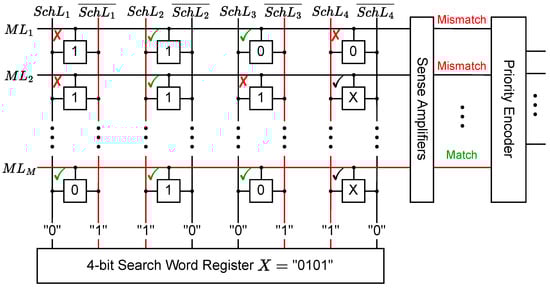
Figure 4.
Structure of an TCAM array. The search word X = “0101” is broadcast up the columns via the corresponding search-line and its complement . During evaluation, since there are bits in the top two rows that directly mismatch with the bits in the search word, match-lines discharge to ground. At , we have a match case and the line remains charged.
The operation of a CAM array is comparable to any operation that requires a search through a table of entries. The main advantage of the CAM structure is that it enables a parallel comparison of the search word with all entries within the array, providing significant speed-up to search operations. The literature has presented CAM implementations on Field-Programmable Logic Arrays (FPGAs) [55,56], and several works have explored the use of NVMs in CAM arrays [57,58,59].
2.3. Architecture Level
The architecture level encompasses the organization of PEs in a tiered hierarchy with supporting interconnect circuitry. Each tier consists of architectural ’blocks’, interconnects, and driving circuits that coordinate the flow of data to each block. An example of a generalized organization of architectural blocks is found in NVSim [20], although we note that other designs may use different naming conventions for their divisions. Figure 5 illustrates the convention used in NVSim. The smallest unit is the PE, denoted as a subarray. Collections of subarrays and driving circuits are organized into larger blocks called mats. Collections of mats are organized into banks, forming a three-tier hierarchy that can handle a collection of banks. For interconnections at the bank level, NVSim provides the option of H-tree or bus-like routing. Of course, architects are not limited to this exact convention: they have the freedom to add or remove levels as desired for their designs, following their own naming conventions to fit their needs.
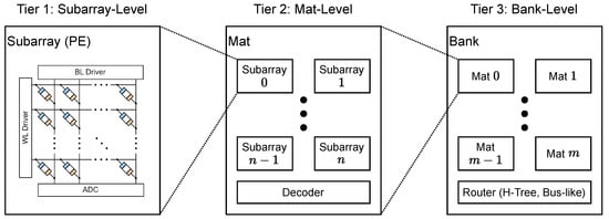
Figure 5.
Structure of architectural blocks in NVSim [20]. A PE (pictured here as a crossbar) would be denoted as a ‘subarray’. Groups of subarrays form mats, and groups of mats form banks.
At this stage, the hardware architecture begins to take form as the designer begins to consider how to connect PEs together and how to scale their overall design. By defining this organization, the designer can focus on how their architecture performs complex operations. RowClone [6] and Ambit [7] are excellent examples of this as they enable the bulk copying of data and bit-wise logical operations across entire rows, respectively. Additionally, ISAAC [10] and RAELLA [11] realize vector–matrix multiplication (VMM) by utilizing the MAC operation from crossbar arrays. Designers have freedom at this level to define how data are processed for their desired application.
It is here where most NVM simulators, such as NVSim and NVMain, reach their limit without modification to support higher levels of simulation. Most CiM simulators will utilize one of these tools to specify an architecture to simulate, which can prevent designers from utilizing that higher-level framework for their own designs without significant modification. For instance, the NeuroSim series of works [25,60,61,62] comprise higher-level engines that take advantage of the underlying NeuroSim framework by defining specific architectures for each high-level application.
2.4. System/Algorithm Level
The system/algorithm level serves as the mapping between the software/application and the hardware/architecture. Given an application and the hardware structure, this level considers the scheduling of operations such that they are executed optimally in the architecture. The decision of the instruction set architecture (ISA) and how it is compiled will ultimately determine how the application code is converted into a set of instructions, which can affect various performance metrics. Simulation at this level can be crucial in identifying algorithmic optimizations that can affect lower-level efficiency and thus enhance higher-level performance.
Several works describe frameworks focusing on this level. PIMSim [26] focuses on PIM instruction offloading to optimize instruction-level performance. PIMulator-NN [28] provides a means to map a DNN model to one of the predefined architectures. In many cases, architecture-level simulators may not provide a means for a designer to evaluate higher-level performance metrics.
2.5. Application Level
The application level represents the highest-level tasks that end users are interested in optimizing. These can include many high-level applications, such as NN acceleration, graph processing, Boolean expression evaluation, and so on. Different applications are better suited for different architectural configurations. For instance, NN acceleration heavily relies on efficient VMM, so architectures like ISAAC [10] and RAELLA [11] are very apt; however, they would not perform as well as MAGIC [13] or IMPLY [14] for Boolean expression evaluation.
Many CiM simulators focus on deriving application-level performance metrics running on predefined architectures. MNSIM 2.0 [31] and the NeuroSim works [25,60,61,62] are examples of this, where the focus has shifted from lower-level to higher-level simulation. Designers who wish to achieve this for other applications would need to start with a lower-level simulator and design interfaces for the algorithm and application levels.
3. Survey Methodology
Designers of hardware accelerators have many options to choose from and many decisions to make throughout the design space levels. Moreover, due to the expensive nature of the fabrication process, designers need an inexpensive means of testing their architectures to obtain the empirical key metrics needed to compare the performance of their design with others. Simulators have provided a solution for this problem, and many more are being added to the literature based on the needs of researchers.
We have collected three classical memory, five NVM, and twelve CiM simulators from the literature to survey. These simulators are well-established tools that have expanded on previous work in this field. For instance, the classical memory simulators CACTI [48], SPICE [47], and gem5 [63] have been used in the field for many years, have undergone several revisions, and have been validated against physical implementations of computer architectures. The NVM memory simulators NVSim [20], NVMain 2.0 [21], and NVMExplorer [22] are either built on top of the principles of the classical memory simulators or are expansions of them that still utilize their file formats. Several CiM simulators have been selected based on their ability to simulate different CiM architectures and NVM devices.
We compare the various capabilities of these simulators across several domains to assess the current simulation environment. Namely, this survey assesses the following:
- the design levels that each simulator explores;
- the NVM devices, and whether or not MLC configurations are supported;
- the circuit designs, including simulation of required peripheral circuitry;
- the architectural configuration options, including routing and more complex structures;
- the supported systems and algorithms, with consideration of their rigidity;
- the currently explored user-level applications.
4. CiM and NVM Simulators
The literature presents several CiM and NVM simulation tools that researchers can utilize to test their designs. Figure 6 illustrates the memory simulator landscape as a web. Traditional memory simulators such as CACTI [64], SPICE [47], and gem5 [63] have significantly influenced the design, development, and validation of NVM and CiM simulation tools. In this section, we thoroughly analyze all twenty simulation tools and explore their features in detail.
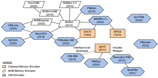
Figure 6.
The collection of simulators reviewed in this work, with their years of release. The edges connecting simulators represent usage or reference of the older work within the newer one. The presented simulator works are CACTI [48], SPICE [47], gem5 [63], NVSim [20], NVMain 2.0 [21], NVMExplorer [22], NVSim-CAM [23], Eva-CAM [24], NeuroSim [25], PIMSim [26], PiMulator [27], PIMulator-NN [28], Ramulator-PIM [29,65,66], MultiPIM [30], MNSIM 2.0 [31], Sim2PIM [32], CIM-SIM [33], PIMSys [34], MICSim [35], and CiMLoop [36].
4.1. Classical Memory Simulators
Here, we provide a brief history of three classical memory simulators (CACTI, SPICE, and gem5) and examine their evolution, noting their applications in CiM and NVM simulation.
4.1.1. CACTI [48,64,67,68]
Originally developed in 1993, CACTI [64] was designed as an analytical tool to estimate access time and cycle time for on-chip caches based on various architectural parameters. The model used in CACTI incorporates load-dependent transistor sizing, rectangular subarray stacking, and column-multiplexed bit-lines to approximate real cache behavior closely. CACTI integrates various cache components, including the tag array, comparators, and word-line drivers to estimate delays based on input parameters such as cache capacity, block size, associativity, technology generation, number of ports, and independent banks.
Over time, CACTI has undergone six major revisions, which expand its capabilities by adding power and area models for fully associative caches, embedded DRAM memories, and commodity DRAM memories. CACTI 4.0 [67] added leakage power modeling to address deep sub-micron trends. Subsequent versions, such as CACTI 6.0 [48], introduced models for Non-Uniform Cache Access (NUCA) and Uniform Cache Access (UCA) architectures, leveraging grid topologies and shared bus designs with low-swing differential wires for large caches [69]. Moreover, CACTI 7.0 [68] offers timing models for Input/Output (I/O) interfaces [70] and 3D die-stacked memories [71]. The tool supports technology nodes down to 16 nm and provides user-defined cache configurations. While older CACTI versions offer a rich design space for cache and DRAM systems, with further modifications they were capable of integrating NVM systems, as shown in [49]. However, the new cascaded channel architecture in [68] expanded CACTI’s applicability to modern memory architectures, enabling advanced DSE for hybrid DRAM/NVM systems.
4.1.2. SPICE [47]
SPICE is a device-level and circuit-level simulator that is widely used for quick prototyping and simulation of integrated circuits. It was first developed at the University of California, Berkeley by LW Nigel and DO Pederson in 1973 [47]. The simulator was stocked with models that represented diodes, MOSFETs, junction field-effect transistors (JFETs), and bipolar junction transistors (BJTs). The circuit simulation was originally written on a set of punch cards, known as a SPICE deck, and provided metrics for non-linear DC analysis, noise analysis, and transient analysis. With SPICE’s flexibility, designers could implement any analog or digital circuit as desired, up to the maximum supported memory of the computer running SPICE.
Since then, SPICE has been improved and expanded several times in the last fifty years. SPICE decks are now fully digital, and the models have become more sophisticated and more accurate. Today, there exist several SPICE simulation tools, each with varying capabilities, accuracies, and focuses [72]. Some examples include PSpice from Cadence Design Systems [73], HSPICE from Synopsys [74], LTspice from Analog Devices [75], and the open-source tool NGSPICE [76].
4.1.3. gem5 [63]
gem5 is a versatile and modular simulation framework widely used for modeling system-level and architecture-level designs. It supports two primary modes: full-system simulation, which enables the execution of complete operating systems and applications, and system-call emulation, which enables simulation of individual applications by emulating system calls. With support for multiple ISAs, including x86, ARM, and RISC-V, as well as a variety of CPU models, gem5 offers researchers significant flexibility in exploring many architectural configurations. Despite its extensive configurability, gem5 does not natively provide circuit-level or device-level simulation, such as detailed memory cell behavior or emerging NVM technologies. However, gem5 can often be integrated with other simulators to extend its capabilities. For instance, PIMSim [26] leverages gem5 for full-system simulation while providing detailed PIM modeling, allowing comprehensive evaluation of PIM architectures. gem5’s high fidelity can result in slower simulation speeds. Nonetheless, gem5 remains a valuable and widely adopted tool in computer architecture research due to its flexibility, extensibility, and strong community support.
4.2. NVM Simulators
The next five simulators have been specifically tailored to simulate NVM devices by defining their own device models and following the well-established principles of the classical memory simulators to maintain a high level of accuracy at the device level.
4.2.1. NVSim [20]
NVSim is a circuit-level modeling tool developed to estimate area, timing, dynamic energy, and leakage power for both volatile memory and NVM devices. It is built on principles inspired by CACTI [48] and offers flexibility to model emerging NVMs with evolving architectures. It allows users to define detailed memory organizations, including subarrays, mats, and banks, and supports customizable routing schemes, such as H-tree and bus-like connections. NVSim also provides multiple sensing schemes, including current-mode, voltage-mode, and voltage-divider sensing, enabling accurate modeling of read and write operations tailored to specific NVM properties.
The tool incorporates detailed parameters for memory cell design (including MOS-accessed and cross-point structures) and models peripheral circuitry, such as SAs and decoders. NVSim has been validated against industrial NVM prototypes, demonstrating its accuracy in predicting latency, energy, and area metrics, typically within a 30% error margin [20]. While NVSim provides a broad design space, it does not natively support specialized architectures such as CiM systems, and extending the tool for such designs requires significant modifications. For example, the base distribution does not include specialized peripheral circuitry required for CiM, such as ADCs and encoders, leaving designers responsible for creating models compatible with NVSim’s existing framework. Furthermore, designers must map their applications to the architecture using alternative methods as the tool does not provide this functionality. Despite these limitations, NVSim remains a reliable platform for early-stage exploration and optimization of NVM technologies.
4.2.2. NVMain 2.0 [21,77]
NVMain is a cycle-accurate simulator developed to model the architectural behavior of DRAM and emerging NVMs. In its initial release, NVMain [77] offered fundamental capabilities to simulate hybrid memory systems and address endurance challenges in NVM technologies. Although it does not perform circuit-level simulations like SPICE or similar tools, NVMain enables users to integrate energy and timing parameters obtained from tools such as NVSim [20] and CACTI [48]. NVMain faces limitations in flexibility, lacks support for advanced configurations such as MLCs, and does not address subarray-level parallelism or more complex hybrid memory setups. These gaps motivated the development of NVMain 2.0 [21], a more robust and extensible version that not only retained the core capabilities of its predecessor but also introduced significant enhancements to address the growing complexity of memory architectures.
NVMain 2.0 expanded its scope by supporting architecture-level modeling, offering a flexible memory hierarchy with subarrays as its basic building blocks and enabling advanced MLC simulations with precise energy and latency metrics. It featured a modular memory controller with a generalized address translator, allowing for easy customization and support of hybrid memory systems with hardware-based page migration. One of the major improvements allows for seamless integration with simulators such as gem5 [63]. New configurable hooks extended the functionality of NVMain to dynamically monitor, intercept, and modify memory requests at various levels of the hierarchy. Although NVMain 2.0 greatly enhances flexibility and accuracy, it remains constrained to architectural-level simulations, requiring further development for system- and application-level studies. Additionally, its lack of native support for CiM architectures limits its applicability in emerging domains without significant modifications.
4.2.3. NVMExplorer [22]
NVMExplorer is a device-, system-, and application-level framework for evaluating the performance of tasks on different NVMs and classical memory technologies using Pareto Frontier visualizations. This work establishes an extended version of NVSim that adds more types of NVM cells and supports MLCs. A user edits a configuration file to specify an experiment, where they can generate a set of configurations to test. At the device level, the NVM options include FeFET, RRAM, PCM, and STT-MRAM. The process node can also be configured and a user can create customized cell models to add to the existing library. At the system level, the user specifies the total number of reads and writes, the read and write frequency, and the size of the words in the arrays. At the application level, different memory traffic patterns are specified for different applications, such as graph processing, DNNs, and general-purpose computation.
Upon compilation, the user-defined cross-stack configuration is sent to an evaluation engine. The modified NVSim, built to support more NVM devices and MLCs, runs as the core of this engine, generating standard fixed-memory-array architectures for each selected technology, read/write characteristics, and application traffic. For each generated architecture, it performs a simulation and produces statistics on high-level area, performance, reliability, and power consumption. The framework also includes application-level fault injection modeling in the configuration options and provides related statistics. The results are collected in a comma-separated value (CSV) file, providing a comprehensive overview of the application-level performance metrics for each application.
4.2.4. NVSim-CAM [23]
NVSim-CAM is a device- and circuit-level simulation tool that specializes in TCAM arrays that utilize NVM devices. The simulator achieves this by modifying the backbone of NVSim to support the peripheral circuits needed for CAM operations. Due to the nature of different NVM cell designs, the tool provides a flexible interface to specify the ports of the cell, including transistor sizes, wire widths, voltage, and current values. Additionally, the means by which a cell is accessed also determines how the cell charges and discharges. The simulator specifies three access modes to account for several options. For peripheral circuitry, NVSim-CAM expands on NVSim’s options for SAs and provides fixed definitions for the accumulator and priority encoder circuits. Customized SA designs are supported by either providing an HSPICE file or by providing SA data from the literature. The simulator’s results have been validated with fabricated devices representing different NVM technologies and different access modes. The authors utilize their tool to perform DSE and propose a 3D vertical ReRAM TCAM design to demonstrate the flexibility of NVSim-CAM.
4.2.5. Eva-CAM [24]
Eva-CAM is a simulator that operates at the device, circuit, and architecture levels, building upon and extending the capabilities of NVSim-CAM. The tool supports three match types: exact match (EX-match), best match (BE-match), and threshold match (TH-match). By leveraging latency-sensing and voltage-sensing schemes, it models these match types based on the differing discharge rates of the , which depend on the number of cells matching the search word. Furthermore, the simulator includes support for modeling three-terminal NVM devices, enabling their configuration into a CAM array using the same simulation framework.
One of the largest accomplishments of Eva-CAM is the modeling of analog and multi-bit CAM arrays. If a device with variable resistance (such as RRAM, FeFET, or PCM) is used for the memory cell, it enables the cell to store a continuous interval of values. Analog and multi-bit CAM arrays exploit this in order to store and search for smaller ranges of values, each corresponding to a different state. The simulator provides an interface to specify the resistance values, the search voltages, and the write voltages for each desired state.
4.3. CiM Simulators
The final twelve simulators have been heavily tailored to specific architectures, algorithms, and applications. They cover a vast span of modern-day designs and use cases, all at different levels of simulation granularity.
4.3.1. NeuroSim [25,60,61,62]
NeuroSim is a circuit-level macro model designed to evaluate the performance of neuromorphic accelerators by estimating their area, latency, dynamic energy, and leakage power. It enables hierarchical exploration from the device level to the algorithm level, supporting early-stage design optimization of neuro-inspired architectures. Several versions of NeuroSim exist for use with multilayer perceptron (MLP) networks [62], 3D-stacked memories [61], and DNNs [60]. In the latter case, the simulator consists of a Python wrapper and the NeuroSim Core. The wrapper serves as the main interface, operating at the system- and application levels to establish the DNN structure, perform training, and collect inference accuracy metrics. It communicates with the NeuroSim Core—responsible for performing device-, circuit-, and architecture-level simulation—to turn the user configuration into a chip floor-plan and to map the weights to the hardware.
The simulator integrates device properties and NN topologies into its framework, allowing users to evaluate both circuit-level performance and learning accuracy. Inputs to NeuroSim include device parameters, transistor technology nodes, network topology, and array size. NeuroSim is built using methodologies from CACTI [48] for SRAM cache modeling, NVSim [20] for NVM performance estimation, and MNSIM [31] for circuit-level modeling of neuro-inspired architectures. These simulators provided frameworks for estimating area, latency, energy, and circuit-level performance, which NeuroSim extended to support hierarchical modeling and runtime learning accuracy in neuromorphic systems.
4.3.2. PIMSim [26]
PIMSim is a simulator built to study PIM architectures at different levels, from circuits to full systems. It combines multiple memory simulators, such as DRAMSim2 [78], HMCSim [79], and NVMain [21], to model a variety of memory types, including DRAM, Hybrid Memory Cube (HMC), and emerging NVM devices. PIMSim offers different simulation modes (such as fast, instrumentation-driven, and full-system), allowing researchers to balance simulation speed and accuracy based on their needs. The simulator supports PIM-specific instructions, coherence protocols, and dynamic workload partitioning, making it possible to explore how moving computations to the memory unit affects system performance. While its flexibility is a major strength, the setup can be complex, and its full-system simulations tend to be slower than hardware-based tools like PiMulator [27]. Even so, PIMSim is a highly adaptable tool for exploring custom PIM designs and evaluating their potential.
4.3.3. PiMulator [27]
PiMulator is an FPGA-based platform designed to prototype and evaluate PIM architectures with high fidelity and speed. It supports memory systems such as DDR4 and high-bandwidth memory (HBM) and models detailed components, namely subarrays, banks, bank groups, and rows, enabling advanced features like data transfers within banks or between subarrays. PiMulator operates at the circuit level, modeling fine-grained memory behaviors such as bank states and timing, and the architecture level, enabling researchers to implement and evaluate PIM logic and interconnect designs. Using System Verilog and the LiteX [80] framework, PiMulator allows researchers to emulate PIM architectures such as RowClone [6], Ambit [7], and LISA [8], which focus on bulk data copying and in-memory computation. Its FPGA acceleration delivers up to 28× faster performance than traditional software simulations, making it ideal for DSE. Although PiMulator excels at modeling volatile memory systems, it does not natively support NVMs without user extensions.
4.3.4. PIMulator-NN [28]
PIMulator-NN, a simulation framework for PIM-based NN accelerators, introduces a novel event-driven methodology that bridges architecture-level customization and circuit-level precision. The simulator employs an Event-Driven Simulation Core (EDSC), which organizes execution through discrete events and captures the precise behavior of hardware systems, including conflicts like bus or port contention. The simulation process begins with user-provided architecture description files, which detail modules, interconnections, and data-flows. These descriptions are parsed through a front-end interface that converts DNN models into executable flows, enabling hardware–software co-simulation. Back-end integration with tools like NeuroSim [25] facilitates accurate estimations of key parameters such as latency, energy, and area at the circuit level. This modular approach allows users to explore diverse PIM-based designs efficiently by defining architecture templates and execution flows.
Despite its robust capabilities, PIMulator-NN is not without limitations. It lacks an automated compiler for mapping DNN models to arbitrary architectures, necessitating manual intervention for custom designs. Additionally, the simulator does not account for control logic overhead or support comprehensive interconnect modeling beyond bus-based schemes. Nevertheless, its ability to generate detailed architectural metrics, such as power traces and execution latencies, surpasses traditional frameworks reliant on simplified performance models. These strengths make PIMulator-NN particularly suited for exploring trade-offs in architectural optimizations, although its current version remains constrained in addressing system-level complexities like network-on-chip (NoC) modeling and advanced pipeline strategies.
4.3.5. Ramulator-PIM [29,65,66]
Ramulator-PIM is a system- and application-level simulator that aims to compare the performance of an application on CPU and PIM cores. The work was introduced alongside the NAPEL framework [66] and is a combination of ZSim [81] and Ramulator [65]. First, for a given application, the PIM sections are separated into regions of interest within the application code. Then, the user sets up the configuration files and runs ZSim to generate memory trace files. A modified version of Ramulator, which uses a 3D-stacked HMC for the PIM cores, accepts these trace files and runs simulations based on user-defined Ramulator configuration settings. Ramulator can run either a CPU simulation or a PIM core simulation based on which is selected in the configuration file. It cannot run both types of simulations simultaneously.
4.3.6. MultiPIM [30]
MultiPIM is an architecture- and system-level simulator that focuses on the performance characteristics of multi-memory-stack PIM architectures. It is based on the principles found in simulators such as ZSim [81] and Ramulator-PIM [29,65,66]. The simulator consists of a front-end that handles instruction simulation and a back-end that handles memory access simulation. For instruction simulation, the front-end uses ZSim to take on the overhead of non-memory-related instructions and cache accesses. It is possible to replace ZSim with another simulator such as gem5 [63]. For memory access simulation, the principles of Ramulator are employed to handle packet routing in a user-defined memory network topology.
In MultiPIM, memory is organized into vaults (equipped with a cache, a translation lookaside buffer (TLB), and a page table walker (PTW)), which are further organized into memory stacks. This organization enables the simulation of core coherence, multi-threading, and virtual memory in PIM systems. The front-end separates CPU tasks and PIM tasks before handing them to a request dispatcher in the back-end. This dispatcher creates CPU and PIM packets to distribute to the CPU and a series of PIM cores. Users can edit configuration files to adjust the network topology and timing parameters, enabling a thorough analysis of NoC architectural designs.
4.3.7. MNSIM 2.0 [31]
MNSIM 2.0 is a behavior-level modeling tool designed to evaluate PIM architectures, focusing on performance and accuracy optimization for NN computations. It simulates an NN and measures accuracy while accounting for various architecture and device parameters, such as a hierarchical modeling structure, a unified memory array model for consistent evaluation of analog and digital PIM designs, and an interface for PIM-oriented NN training and quantization. MNSIM 2.0 integrates PIM-aware NN training and quantization techniques, such as mixed-precision quantization and energy-efficient weight regularization, to enhance energy efficiency and reduce latency. The simulator provides a fast evaluation framework by bypassing time-consuming circuit simulations during the iterative optimization phases. Validation against fabricated PIM macros demonstrates a low error rate (3.8–5.5%). MNSIM 2.0 focuses primarily on CNN-based applications, with limited support for other DNN algorithms, and its accuracy may be influenced by the granularity of modeled device noise and variations. Additionally, it does not yet include all potential circuit noise models or advanced algorithm mapping strategies.
4.3.8. Sim2PIM [32]
Sim2PIM is an algorithm- and application-level framework capable of simulating interactions between a host processor and a PIM design. The framework consists of two distinct phases, known as the offline instrumentation and the online execution. A static parser is used to implement offline instrumentation, where the host’s resources, such as its hardware performance counter (HPC), provide performance metrics and coordinate multi-threading prior to simulation. The online execution phase separates the PIM simulation from the system-level overhead, allocating physical hardware resources as efficiently as possible to maximize simulation speed. The tool establishes a PIM controller and backbone, a threading interface, and a PIM instruction buffer to achieve efficient coordination between the host application and PIM simulation while also maintaining their isolation.
A PIM simulator is used to execute the PIM instructions as dictated by the PIM controller. The remainder of the online execution system performs the measurement task by accounting for the HPC of the host system. In times where an overhead is necessary that does not pertain to the simulation (such as high-level multi-threading, the writing of instructions to the buffer, and other operations that must occur due to the needs of the physical hardware), the system pauses and resumes HPC monitoring accordingly to ensure accurate measuring of the PIM simulator’s performance in executing the application-level task. This PIM simulator can be any of the lower-level tools previously discussed as long as it adheres to the threading interface’s rules.
4.3.9. CIM-SIM [33]
CIM-SIM is an algorithm-level simulator that coordinates execution of a predefined ISA, named as a nano-instruction set, on crossbar-based Compute-in-Memory with Periphery (CIM-P) tiles. Each CIM-P tile consists of the following: registers for executing instructions such as Write Data (WD), Write Data Select (WDS), Row Select (RS), Column Select (CS), Do Array (DoA), and Do Read (DoR); a nano-controller that handles the incoming nano-instructions; and a calculator tile that houses a CiM crossbar kernel. In their provided example, the crossbar is equipped with the necessary peripheral circuitry (such as digital input modulators (DIMs) and ADCs) as well as some sample-and-hold circuitry to serve as a mediator between the crossbar output and the CIM-P tile readout. The CIM-P tiles also accept a set of Function Select (FS) signals to specify which operation to perform on the kernel.
The work provides example kernels for VMM and bulk bit-wise operations. In both instances, the CIM-P tile undergoes a four-stage process to produce a calculation. In the load phase, the crossbar is programmed using a series of WD and RS instructions. In the configuration phase, the FS signal chooses the desired operation and the WDS and CS instructions specify which rows and columns will take place in the operation. In the compute phase, the DoA instruction is passed to activate the DIMs, and data are written or computed by the array, with the result being routed to the sample-and-hold registers. Finally, in the read phase, the DR instruction passes the data to the ADCs, producing a digital output signal of the result. Other crossbar-based kernel operations can be implemented by writing instruction-set-level algorithms that follow the same flow.
4.3.10. PIMSys [34]
PIMSys is a system- and application-level simulator specifically designed to simulate the intricacies of Samsung’s PIM-HBM [38] design for NN applications. Primarily, this simulator focuses on the interactions between PIM-HBM and a host processor, which supports both normal and PIM modes of operation. To accurately model the memory system, the tool extends a version of DRAMSys [38] to include the architectural design of a processing unit, consisting of bank interfaces, register files, and floating-point units for addition and multiplication. In doing so, the tool models the functional behavior of PIM-HBM in line with the DRAM timing parameters specified by DRAMSys.
To model the interaction of the memory model with a host, gem5 is utilized to model the processor and its caches. This host generates memory requests based on a compiled binary, where these requests control the modes of operation for PIM-HBM. The authors developed a software library that allows users to write programs that control the processing units. To illustrate the speedup that PIM workloads experience under PIM-HBM, a comparison of vector addition, multiplication, and VMM is conducted between normal and PIM modes.
4.3.11. MICSim [35]
MICSim is a full-stack simulation tool that focuses on providing flexibility for a variety of mixed-signal (e.g., crossbar) CiM designs for CNN and Transformer applications. It extends on the capabilities of NeuroSim [25] by creating a Python interface, which establishes modules for each step of the NN models and interacts with popular NN frameworks and libraries such as PyTorch and HuggingFace Transformers. The tool separates the tasks of weight quantization with Quantizer/Dequantizer modules, digit composition with DigitDecomposer/DigitAssembler modules, and signal conversion with Digit2Cell/DAC/ADC modules. In this manner, users can tailor each module based on how their specific design handles each of these areas. In addition, this modularization reduces the non-ideal effects that mixed-signal designs have on the software’s performance.
For hardware evaluation, MICSim provides a Python wrapping of the circuit modules specified by NeuroSim, which enables researchers to specify their circuit designs in object-oriented Python code that adheres to the architectural model of NeuroSim. In addition, the tool utilizes a data-averaging mode to replace the memory-intensive and time-consuming trace-based mode of NeuroSim. This averaging mode computes the average ratio of non-zero elements in the set of input vectors and the average conductances (i.e., the reciprocal of resistances) of the cells in the subarray, then scales the calculation by the number of input vectors. The trade-off of simulation accuracy in favor of faster runtimes produces a to speedup in comparison to NeuroSim.
4.3.12. CiMLoop [36]
CiMLoop is a flexible modeling tool for NN applications. It utilizes a framework that combines the area and energy estimations of Accelergy [82] with the full-system analyses provided by Timeloop [83] and extends these tools to support CiM designs. A CiM design is specified with a YAML file consisting of a hierarchy of containers. Each container can be defined to consist of a combination of devices, circuits, and other containers. For example, one column of a crossbar array can be specified as a container of cells and an SA/ADC, and then instances of that container can be composed to form a larger container that represents the entire subarray. This allows for a flexible and simple means of specifying many different architectures.
For modeling individual devices and circuits, CiMLoop provides plug-ins for different models provided by other simulation tools, such as CACTI [68], NVMExplorer [22], and NeuroSim [25]. In doing so, this allows researchers to fairly evaluate models and designs across different works within the simulation space. To provide fast runtimes, the tool averages the energy calculation by component such that the average energy each component uses can be calculated in constant time. By parallelizing these calculations, energy metrics for entire architectures can be simulated in reasonable amounts of time.
5. Discussion and Comparison
Currently, for a new design to be simulated accurately, researchers must search the simulator space for one that best matches their use case. Then, after selecting a simulator, researchers need to create the modifications necessary to map their architecture to the simulator. In some cases, this task can be as simple as changing a few values in a configuration file; in other cases, it can be as difficult as altering or extending the existing code, where it may become necessary to write entirely new libraries. The latter case usually results in the creation of a new simulator (e.g., the extension for CAM arrays that NVSim-CAM [23] provides for NVSim [20]) to further enhance the DSE of a specific design for a specific application.
There are many simulators that have been proposed in the literature, but they are not all-encompassing. Each simulator is tailored to meet specific goals necessary for analyzing specific designs at their respective levels. While it may be possible to use one simulator to model all levels, it may become impractical due to long runtimes, limited resources, and programming complexity. We define the scope of a simulator to represent the primary design levels the simulator focuses on. Table 2 summarizes the design level scopes that the classical, NVM, and CiM simulators currently provide. NVMExplorer [22], NeuroSim [25], MNSIM 2.0 [31], MICSim [35], and CiMLoop [36] achieve a full cross-level scope.
Table 2.
Design level scopes of classical, NVM, and CiM simulators.
Additionally, the simulation space faces a trade-off challenge with respect to accuracy and runtime. To produce accurate results, more time is required to perform the necessary computations. Some simulators provide options for researchers to specify optimization targets and filter out designs that do not meet their performance criteria. PIMSim [26] offers different simulation modes that trade accuracy for runtime. NVSim [20] provides configuration options for optimization targets. MICSim [35] uses an averaging mode versus a trace-based mode, favoring faster runtimes over precise simulation metrics. CiMLoop [36] relies on a data-distribution-based model to avoid the runtime cost of running a DNN on top of modeling the full system. In general, simulators with a focus on devices and circuits lean more toward maintaining accuracy, while higher-level simulation tools trade off this level of accuracy to ensure simulation runtime remains feasible.
We discuss the state of the simulator environment based on what has been explored in the literature. With researchers seeking to obtain a view of their design’s performance across all design levels, we witness the need for a solution that spans the entire design space and provides flexibility to accommodate as many designs as possible.
5.1. Supported Devices
The promise shown by emerging NVM devices facilitates the need to explore different devices and understand their behavior and intrinsic characteristics. Many CiM works [9,10,11,12,13,14,15] utilize NVM devices as they enable new methods of computation that are not possible to perform on contemporary devices. The ideal simulator provides a means to test a suite of device technologies and compare them with each other across design metrics.
Table 3 provides details on the supported NVM devices of the simulators presented. Unsurprisingly, NVM simulators supply several models for different device technologies, so they provide an excellent means of obtaining device-level metrics. However, we observe that higher-level simulators restrict this configurability, even if they use an NVM simulator as a backbone. NeuroSim [25], PIMulator-NN [28], and MNSIM 2.0 [31] focus specifically on NN accelerator designs involving RRAM devices, with the first two drawing from the principles of NVSim [20] for their device modeling. If a researcher was interested in investigating a crossbar design with a different device for the same application, they would need to configure the memory simulator to model that device instead. This can result in changes that propagate up the design space levels, requiring further modification.
Table 3.
Configurable NVM devices and MLC support of memory simulators.
5.2. Supported Circuits
There are many possible ways that devices and peripheral circuits can be combined to form PEs. With many different memory array configurations and with new designs being proposed frequently, it can be challenging to locate a simulator that provides enough flexibility to easily specify a design. The ideal simulator not only provides a standard set of frequently used configurations but also a means of introducing new designs for arrays and peripheral circuits.
Table 4 presents the circuits that memory simulators can currently simulate without modification. With the cases of NVMExplorer [22], NVSim-CAM [23], and Eva-CAM [24], we observe restrictions in the circuit designs. Although NVMExplorer [22] is capable of simulating standard RAM arrays, and both NVSim-CAM [23] and Eva-CAM [24] are capable of simulating CAMs, the user does not explicitly have the option to configure the array in a flexible manner. Should a researcher find a need to alter the array organization to comply with their design, they would need to alter and potentially expand on the code to include any peripheral circuits that have not been provided. This can be time-consuming as the new code needs to fit well within the existing model to provide accurate metrics.
Table 4.
Modeled circuits within memory simulators.
5.3. Supported Architectures
Establishing the hierarchy of PEs, subarrays, banks, mats, and other architectural blocks is crucial for the scaling of a design. The means by which blocks communicate and coordinate greatly affects system- and application-level performance. Many designs incorporate different levels of block collections, may assign different names to each level, and may connect them all together differently. For instance, a three-tier architecture may organize PEs together into a subarray, then organize subarrays together into a bank using an H-tree interconnect for all the tiers; however, that naming convention may not hold for a four-tier architecture with PEs organized into subarrays, subarrays organized into mats, and then mats into banks using a bus-like interconnect. The ideal simulator would provide enough flexibility to construct an architecture of many tiers, where the user can specify the naming conventions they wish to use and how to connect blocks together.
Table 5 displays the architectural organizations that current simulators can support. Despite full customization, SPICE [47] at this level begins to slow down drastically, making it impractical for architecture-level analyses [31]. NVSim [20] provides the most flexibility, with options to organize PEs into a three-tier subarray–mat–bank structure. Many of the simulators in the literature focus on simulating a specific architecture, with little room for adjustment without significant modification to the source code at lower design levels. Consequently, it is difficult to compare different organizations of blocks without creating a new simulator.
Table 5.
Configurable architectural elements within memory simulators.
5.4. Supported Systems and Algorithms
Underneath all the high-level applications of computing systems are the algorithms that leverage the hardware they run on. An algorithm can only run as fast as the hardware allows, so it is crucial for researchers to understand which architectures are suitable to achieve a given task as efficiently as possible. The ideal simulator provides a way to study a set of architectures and measure their performance on system- and algorithm-level tasks.
Table 6 shows which systems and algorithms are supported by the memory simulator environment. We observe that a broad spectrum of simulators focus on VMM workloads as VMM is essential for DNN inference and training. PIMSim [26], PiMulator [27], Sim2PIM [32], and CIM-SIM [33] instead focus on mapping CiM ISAs onto current hardware as a means of efficiently collecting simulation data for CiM systems that work with CPUs. To perform similar analyses for different architectures and applications, researchers are left with the task of developing their own tools, either by adapting one of these tools or by starting with a lower-level simulator and building upward.
Table 6.
Configurable systems and algorithms of memory simulators.
5.5. Supported Applications
All computing architectures are designed with the purpose of fulfilling a specific goal or task as efficiently as possible. High-level applications ultimately need to meet the demands of the end user, and many of these applications require different kinds of workloads. The ideal simulator provides a way for architects to explore the applications for which their designs are best suited and to identify the presence of bottlenecks throughout all design levels.
Table 7 presents some of the high-level applications of memory simulators. This listing is not encompassing of all types of applications; many of the simulators tend toward focusing on NN applications and data-flow analysis. MNSIM 2.0 [31], Sim2PIM [32], and CIM-SIM [33] lean more towards the analysis of bulk bit-wise operations, but they are not as flexible when it comes to lower-level design choices. NVMExplorer [22] allows for the selection of a set of read/write traffic patterns within the memory unit; however, the researcher must obtain those patterns first, usually with the aid of a lower-level simulator separately.
Table 7.
Configurable applications of memory simulators.
6. Conclusions
In this paper, we have obtained an image of the NVM and CiM simulation landscape, which presents many opportunities for further research. We have seen that the DSE of CiM architectures is far from completion, and researchers are in need of tools to expand their search for effective designs. To conclude, we briefly summarize the gaps in the simulation space with respect to DSE.
- Standardization. Quantitative analyses on the accuracy and efficiency of these simulators present difficulty. Not only are they all designed with different focuses and applications in mind but they also utilize different foundational principles originating from CACTI [48], SPICE [47], and gem5 [63]. Architects are presented with many choices but not exactly reassurance on whether or not a given simulator can meet their needs. In some cases, it can be difficult to discern the capabilities and limitations of these tools. The establishment of a benchmark or standard would allow researchers to better organize these simulators and help them make the best decision on which tools to use.
- Flexibility. Simulators that achieve a full cross-level scope show a great deal of promise in providing a means of evaluating an architecture across all design levels. However, they are presently restrictive to the designs and analyses presented in their respective works. Enabling these works to accommodate more devices, circuits, architectures, systems, and applications can significantly enhance DSE.
- Time consumption. The design space is vast, with many different possibilities to explore. Architects need tools that are capable of searching this space within reasonable amounts of time. While a flexible simulator can provide as much freedom as the architect desires on lower design levels, such freedom is constrained by the amount of simulation time needed to perform higher-level analyses.
- Ease of use. Across each of the simulator works, there are different standards of documenting their tool’s usage. Some tools, such as NeuroSim [25], PiMulator [27], and MNSIM 2.0, [31] provide manuals within their source code that elaborate on details not covered in their published works; others may only provide their publication as their documentation. Establishing a practice of detailed code documentation and means of minimizing the required amount of code modification will allow architects to shift more of their focus to DSE.
Author Contributions
Conceptualization, J.T.M. and D.A.R.; data curation, J.T.M.; funding acquisition, D.A.R.; investigation, J.T.M., A.M.M.A., P.K., and S.H.M.; methodology, J.T.M.; project administration, J.T.M.; supervision, D.A.R.; validation, J.T.M. and D.A.R.; visualization, J.T.M.; writing—original draft, J.T.M., A.M.M.A., P.K., and S.H.M.; writing—review and editing, J.T.M. and D.A.R. All authors have read and agreed to the published version of the manuscript.
Funding
This material is based upon work supported by the National Science Foundation under Grant Number 2347019.
Acknowledgments
We would like to thank Hao Zheng for his guidance in the conceptualization of this paper.
Conflicts of Interest
The authors declare no conflicts of interest. Any opinions, findings, and conclusions or recommendations expressed in this material are those of the author(s) and do not necessarily reflect the views of the National Science Foundation.
Abbreviations
The following abbreviations are used in this manuscript and are sorted alphabetically:
| 1R | 1-Resistor |
| 1T1R | 1-Transistor–1-Resistor |
| 2T2R | 2-Transistor–2-Resistor |
| ADC | Analog-to-Digital Converter |
| AES | Advanced Encryption Standard |
| ALU | Arithmetic Logic Unit |
| BJT | Bipolar Junction Transistor |
| BL | Bit-Line |
| CF | Conductive Filament |
| CiM | Computing-in-Memory |
| CNN | Convolutional Neural Network |
| CMOS | Complementary Metal-Oxide Semiconductor |
| CPU | Central Processing Unit |
| DAC | Digital-to-Analog Converter |
| DIM | Digital Input Modulator |
| DNN | Deep Neural Network |
| DRAM | Dynamic Random Access Memory |
| DSE | Design Space Exploration |
| FeFET | Ferroelectric Field-Effect Transistor |
| FPGA | Field-Programmable Logic Array |
| HBM | High-Bandwidth Memory |
| HMC | Hybrid Memory Cube |
| HPC | Hardware Performance Counter |
| HRS | High-Resistance State |
| I/O | Input/Output |
| ISA | Instruction Set Architecture |
| JFET | Junction Field-Effect Transistor |
| LRS | Low-Resistance State |
| MAC | Multiply–Accumulate |
| MIM | Metal–Insulator–Metal |
| ML | Match-Line |
| MLC | Multi-Level Cell |
| MLP | Multilayer Perceptron |
| MOSFET | Metal-Oxide-Semiconductor Field-Effect Transistor |
| MRAM | Magnetoresistive Random Access Memory |
| MTJ | Magnetic Tunnel Junction |
| NN | Neural Network |
| NoC | Network on Chip |
| NUCA | Non-Uniform Cache Access |
| NVM | Nonvolatile Memory |
| PCM | Phase Change Memory |
| PE | Processing Element |
| PIM | Processing-In-Memory |
| PTW | Page Table Walker |
| RRAM/ReRAM | Resistive Random Access Memory |
| SA | Sense Amplifier |
| SL | Sense-Line |
| SchL | Search-Line |
| SOT-MRAM | Spin–Orbit Torque Magnetoresistive Random Access Memory |
| SRAM | Static Random Access Memory |
| STT-MRAM | Spin–Transfer Torque Magnetoresistive Random Access Memory |
| (T)CAM | (Ternary) Content-Addressable Memory |
| TLB | Translation Lookaside Buffer |
| UCA | Uniform Cache Access |
| VMM | Vector–Matrix Multiplication |
| WL | Word-Line |
References
- Chen, Y.; Xie, Y.; Song, L.; Chen, F.; Tang, T. A Survey of Accelerator Architectures for Deep Neural Networks. Engineering 2020, 6, 264–274. [Google Scholar] [CrossRef]
- Mittal, S. A survey on modeling and improving reliability of DNN algorithms and accelerators. J. Syst. Archit. 2020, 104, 101689. [Google Scholar] [CrossRef]
- Li, G.; Hari, S.K.S.; Sullivan, M.; Tsai, T.; Pattabiraman, K.; Emer, J.; Keckler, S.W. Understanding error propagation in deep learning neural network (DNN) accelerators and applications. In Proceedings of the International Conference for High Performance Computing, Networking, Storage and Analysis, New York, NY, USA, 12–17 November 2017. SC ’17. [Google Scholar] [CrossRef]
- Radamson, H.H.; Zhu, H.; Wu, Z.; He, X.; Lin, H.; Liu, J.; Xiang, J.; Kong, Z.; Xiong, W.; Li, J.; et al. State of the Art and Future Perspectives in Advanced CMOS Technology. Nanomaterials 2020, 10, 1555. [Google Scholar] [CrossRef]
- Mutlu, O.; Ghose, S.; Gómez-Luna, J.; Ausavarungnirun, R. A Modern Primer on Processing in Memory. In Emerging Computing: From Devices to Systems: Looking Beyond Moore and Von Neumann; Springer: Singapore, 2023; pp. 171–243. [Google Scholar] [CrossRef]
- Seshadri, V.; Kim, Y.; Fallin, C.; Lee, D.; Ausavarungnirun, R.; Pekhimenko, G.; Luo, Y.; Mutlu, O.; Gibbons, P.B.; Kozuch, M.A.; et al. RowClone: Fast and energy-efficient in-DRAM bulk data copy and initialization. In Proceedings of the 2013 46th Annual IEEE/ACM International Symposium on Microarchitecture (MICRO), Davis, CA, USA, 7–11 December 2013; pp. 185–197. [Google Scholar]
- Seshadri, V.; Lee, D.; Mullins, T.; Hassan, H.; Boroumand, A.; Kim, J.; Kozuch, M.A.; Mutlu, O.; Gibbons, P.B.; Mowry, T.C. Ambit: In-memory accelerator for bulk bitwise operations using commodity DRAM technology. In Proceedings of the 50th Annual IEEE/ACM International Symposium on Microarchitecture, New York, NY, USA, 14–18 October 2017; MICRO-50 ’17. pp. 273–287. [Google Scholar] [CrossRef]
- Chang, K.K.; Nair, P.J.; Lee, D.; Ghose, S.; Qureshi, M.K.; Mutlu, O. Low-Cost Inter-Linked Subarrays (LISA): Enabling fast inter-subarray data movement in DRAM. In Proceedings of the 2016 IEEE International Symposium on High Performance Computer Architecture (HPCA), Barcelona, Spain, 12–16 March 2016; pp. 568–580. [Google Scholar] [CrossRef]
- Li, S.; Xu, C.; Zou, Q.; Zhao, J.; Lu, Y.; Xie, Y. Pinatubo: A processing-in-memory architecture for bulk bitwise operations in emerging non-volatile memories. In Proceedings of the 53rd Annual Design Automation Conference, New York, NY, USA, 5–9 June 2016. DAC ’16. [Google Scholar] [CrossRef]
- Shafiee, A.; Nag, A.; Muralimanohar, N.; Balasubramonian, R.; Strachan, J.P.; Hu, M.; Williams, R.S.; Srikumar, V. ISAAC: A convolutional neural network accelerator with in-situ analog arithmetic in crossbars. In Proceedings of the 43rd International Symposium on Computer Architecture, Seoul, Republic of Korea, 18–22 June 2016; IEEE Press: Piscatway, NJ, USA, 2016. ISCA ’16. pp. 14–26. [Google Scholar] [CrossRef]
- Andrulis, T.; Emer, J.S.; Sze, V. RAELLA: Reforming the Arithmetic for Efficient, Low-Resolution, and Low-Loss Analog PIM: No Retraining Required! In Proceedings of the 50th Annual International Symposium on Computer Architecture, Orlando, FL, USA, 17–21 June 2023; ACM: New York, NY, USA, 2023. ISCA ’23. [Google Scholar] [CrossRef]
- Long, Y.; Lee, E.; Kim, D.; Mukhopadhyay, S. Flex-PIM: A Ferroelectric FET based Vector Matrix Multiplication Engine with Dynamical Bitwidth and Floating Point Precision. In Proceedings of the 2020 International Joint Conference on Neural Networks (IJCNN), Glasgow, UK, 19–25 July 2020; pp. 1–8. [Google Scholar] [CrossRef]
- Kvatinsky, S.; Belousov, D.; Liman, S.; Satat, G.; Wald, N.; Friedman, E.G.; Kolodny, A.; Weiser, U.C. MAGIC—Memristor-Aided Logic. IEEE Trans. Circuits Syst. Ii Express Briefs 2014, 61, 895–899. [Google Scholar] [CrossRef]
- Kvatinsky, S.; Satat, G.; Wald, N.; Friedman, E.G.; Kolodny, A.; Weiser, U.C. Memristor-Based Material Implication (IMPLY) Logic: Design Principles and Methodologies. IEEE Trans. Very Large Scale Integr. (VLSI) Syst. 2014, 22, 2054–2066. [Google Scholar] [CrossRef]
- Angizi, S.; He, Z.; Awad, A.; Fan, D. MRIMA: An MRAM-Based In-Memory Accelerator. IEEE Trans. Comput. Aided Des. Integr. Circuits Syst. 2020, 39, 1123–1136. [Google Scholar] [CrossRef]
- Sun, Z.; Kvatinsky, S.; Si, X.; Mehonic, A.; Cai, Y.; Huang, R. A full spectrum of computing-in-memory technologies. Nat. Electron. 2023, 6, 823–835. [Google Scholar] [CrossRef]
- Akram, A.; Sawalha, L. A Survey of Computer Architecture Simulation Techniques and Tools. IEEE Access 2019, 7, 78120–78145. [Google Scholar] [CrossRef]
- Hwang, I.; Lee, J.; Kang, H.; Lee, G.; Kim, H. Survey of CPU and memory simulators in computer architecture: A comprehensive analysis including compiler integration and emerging technology applications. Simul. Model. Pract. Theory 2025, 138, 103032. [Google Scholar] [CrossRef]
- Staudigl, F.; Merchant, F.; Leupers, R. A Survey of Neuromorphic Computing-in-Memory: Architectures, Simulators, and Security. IEEE Des. Test 2022, 39, 90–99. [Google Scholar] [CrossRef]
- Dong, X.; Xu, C.; Xie, Y.; Jouppi, N.P. NVSim: A Circuit-Level Performance, Energy, and Area Model for Emerging Nonvolatile Memory. IEEE Trans. Comput. Aided Des. Integr. Circuits Syst. 2012, 31, 994–1007. [Google Scholar] [CrossRef]
- Poremba, M.; Zhang, T.; Xie, Y. NVMain 2.0: A User-Friendly Memory Simulator to Model (Non-)Volatile Memory Systems. IEEE Comput. Archit. Lett. 2015, 14, 140–143. [Google Scholar] [CrossRef]
- Pentecost, L.; Hankin, A.; Donato, M.; Hempstead, M.; Wei, G.Y.; Brooks, D. NVMExplorer: A Framework for Cross-Stack Comparisons of Embedded Non-Volatile Memories. In Proceedings of the 2022 IEEE International Symposium on High-Performance Computer Architecture (HPCA), Seoul, Republic of Korea, 2–6 April 2022; pp. 938–956. [Google Scholar] [CrossRef]
- Li, S.; Liu, L.; Gu, P.; Xu, C.; Xie, Y. NVSim-CAM: A circuit-level simulator for emerging nonvolatile memory based Content-Addressable Memory. In Proceedings of the 2016 IEEE/ACM International Conference on Computer-Aided Design (ICCAD), Austin, TX, USA, 7–10 December 2016; pp. 1–7. [Google Scholar] [CrossRef]
- Liu, L.; Sharifi, M.M.; Rajaei, R.; Kazemi, A.; Ni, K.; Yin, X.; Niemier, M.; Hu, X.S. Eva-CAM: A Circuit/Architecture-Level Evaluation Tool for General Content Addressable Memories. In Proceedings of the 2022 Design, Automation & Test in Europe Conference & Exhibition (DATE), Antwerp, Belgium, 14–23 March 2022; pp. 1173–1176. [Google Scholar] [CrossRef]
- Chen, P.Y.; Peng, X.; Yu, S. NeuroSim: A Circuit-Level Macro Model for Benchmarking Neuro-Inspired Architectures in Online Learning. IEEE Trans. Comput.-Aided Des. Integr. Circuits Syst. 2018, 37, 3067–3080. [Google Scholar] [CrossRef]
- Xu, S.; Chen, X.; Wang, Y.; Han, Y.; Qian, X.; Li, X. PIMSim: A Flexible and Detailed Processing-in-Memory Simulator. IEEE Comput. Archit. Lett. 2019, 18, 6–9. [Google Scholar] [CrossRef]
- Mosanu, S.; Sakib, M.N.; Tracy, T.; Cukurtas, E.; Ahmed, A.; Ivanov, P.; Khan, S.; Skadron, K.; Stan, M. PiMulator: A Fast and Flexible Processing-in-Memory Emulation Platform. In Proceedings of the 2022 Design, Automation & Test in Europe Conference & Exhibition (DATE), Antwerp, Belgium, 14–23 March 2022; pp. 1473–1478. [Google Scholar] [CrossRef]
- Zheng, Q.; Li, X.; Guan, Y.; Wang, Z.; Cai, Y.; Chen, Y.; Sun, G.; Huang, R. PIMulator-NN: An Event-Driven, Cross-Level Simulation Framework for Processing-In-Memory-Based Neural Network Accelerators. IEEE Trans. Comput. Aided Des. Integr. Circuits Syst. 2022, 41, 5464–5475. [Google Scholar] [CrossRef]
- Gómez-Luna, J.; Oliveira, G. ZSim+Ramulator—A Processing-in-Memory Simulation Framework. 2019. Available online: https://github.com/CMU-SAFARI/ramulator-pim (accessed on 23 November 2024).
- Yu, C.; Liu, S.; Khan, S. MultiPIM: A Detailed and Configurable Multi-Stack Processing-In-Memory Simulator. IEEE Comput. Archit. Lett. 2021, 20, 54–57. [Google Scholar] [CrossRef]
- Zhu, Z.; Sun, H.; Xie, T.; Zhu, Y.; Dai, G.; Xia, L.; Niu, D.; Chen, X.; Hu, X.S.; Cao, Y.; et al. MNSIM 2.0: A Behavior-Level Modeling Tool for Processing-In-Memory Architectures. IEEE Trans. Comput.-Aided Des. Integr. Circuits Syst. 2023, 42, 4112–4125. [Google Scholar] [CrossRef]
- Forlin, B.E.; Santos, P.C.; Becker, A.E.; Alves, M.A.; Carro, L. Sim2PIM: A complete simulation framework for Processing-in-Memory. J. Syst. Archit. 2022, 128, 102528. [Google Scholar] [CrossRef]
- BanaGozar, A.; Vadivel, K.; Stuijk, S.; Corporaal, H.; Wong, S.; Lebdeh, M.A.; Yu, J.; Hamdioui, S. CIM-SIM: Computation In Memory SIMuIator. In Proceedings of the 22nd International Workshop on Software and Compilers for Embedded Systems, New York, NY, USA, 27–28 May 2019; SCOPES ’19. pp. 1–4. [Google Scholar] [CrossRef]
- Christ, D.; Steiner, L.; Jung, M.; Wehn, N. PIMSys: A Virtual Prototype for Processing in Memory. In Proceedings of the 10th International Symposium on Memory Systems, MEMSYS, Washington, DC, USA, 30 September–2 October 2024; Volume 2024. [Google Scholar]
- Wang, C.; Chen, Z.; Huang, S. MICSim: A Modular Simulator for Mixed-signal Compute-in-Memory based AI Accelerator. In Proceedings of the 30th Asia and South Pacific Design Automation Conference, New York, NY, USA, 20–23 January 2025; ASPDAC ’25. pp. 541–547. [Google Scholar] [CrossRef]
- Andrulis, T.; Emer, J.S.; Sze, V. CiMLoop: A Flexible, Accurate, and Fast Compute-In-Memory Modeling Tool. In Proceedings of the 2024 IEEE International Symposium on Performance Analysis of Systems and Software (ISPASS), Indianapolis, IN, USA, 5–7 May 2024; pp. 10–23. [Google Scholar] [CrossRef]
- Chung, K.Y.; Kim, H.; An, Y.; Seong, K.; Shin, D.h.; Baek, K.H.; Shim, Y. 8T-SRAM based Process-In-Memory (PIM) System with Current Mirror for accurate MAC operation. IEEE Access 2024, 12, 24254–24261. [Google Scholar] [CrossRef]
- Lee, S.; Kang, S.h.; Lee, J.; Kim, H.; Lee, E.; Seo, S.; Yoon, H.; Lee, S.; Lim, K.; Shin, H.; et al. Hardware Architecture and Software Stack for PIM Based on Commercial DRAM Technology: Industrial Product. In Proceedings of the 2021 ACM/IEEE 48th Annual International Symposium on Computer Architecture (ISCA), Valencia, Spain, 14–18 June 2021; pp. 43–56. [Google Scholar] [CrossRef]
- Lee, H.; Kim, M.; Min, D.; Kim, J.; Back, J.; Yoo, H.; Lee, J.H.; Kim, J. 3D-FPIM: An Extreme Energy-Efficient DNN Acceleration System Using 3D NAND Flash-Based In-Situ PIM Unit. In Proceedings of the 2022 55th IEEE/ACM International Symposium on Microarchitecture (MICRO), Chicago, IL, USA, 1–5 October 2022; pp. 1359–1376. [Google Scholar] [CrossRef]
- Li, H.; Wu, T.F.; Mitra, S.; Wong, H.S.P. Resistive RAM-Centric Computing: Design and Modeling Methodology. IEEE Trans. Circuits Syst. Regul. Pap. 2017, 64, 2263–2273. [Google Scholar] [CrossRef]
- Wang, H.; Yan, X. Overview of Resistive Random Access Memory (RRAM): Materials, Filament Mechanisms, Performance Optimization, and Prospects. Phys. Status Solidi (Rrl) Rapid Res. Lett. 2019, 13, 1900073. [Google Scholar] [CrossRef]
- Apalkov, D.; Dieny, B.; Slaughter, J.M. Magnetoresistive Random Access Memory. Proc. IEEE 2016, 104, 1796–1830. [Google Scholar] [CrossRef]
- Burr, G.W.; Breitwisch, M.J.; Franceschini, M.; Garetto, D.; Gopalakrishnan, K.; Jackson, B.; Kurdi, B.; Lam, C.; Lastras, L.A.; Padilla, A.; et al. Phase change memory technology. J. Vac. Sci. Technol. B 2010, 28, 223–262. [Google Scholar] [CrossRef]
- Reis, D.; Niemier, M.; Hu, X.S. Computing in memory with FeFETs. In Proceedings of the International Symposium on Low Power Electronics and Design, New York, NY, USA, 23–25 July 2018. ISLPED ’18. [Google Scholar] [CrossRef]
- Zahoor, F.; Azni Zulkifli, T.Z.; Khanday, F.A. Resistive Random Access Memory (RRAM): An Overview of Materials, Switching Mechanism, Performance, Multilevel Cell (mlc) Storage, Modeling, and Applications. Nanoscale Res. Lett. 2020, 15, 90. [Google Scholar] [CrossRef] [PubMed]
- Ma, T.; Gong, N. Retention and Endurance of FeFET Memory Cells. In Proceedings of the 2019 IEEE 11th International Memory Workshop (IMW), Monterey, CA, USA, 12–15 May 2019; pp. 1–4. [Google Scholar] [CrossRef]
- Nagel, L.W.; Pederson, D. SPICE (Simulation Program with Integrated Circuit Emphasis); Technical Report UCB/ERL M382; EECS Department, University of California: Berkeley, CA, USA, 1973. [Google Scholar]
- Muralimanohar, N.; Balasubramonian, R.; Jouppi, N.P. CACTI 6.0: A tool to model large caches. HP Lab. 2009, 27, 28. [Google Scholar]
- Arcaro, S.; Di Carlo, S.; Indaco, M.; Pala, D.; Prinetto, P.; Vatajelu, E.I. Integration of STT-MRAM model into CACTI simulator. In Proceedings of the 2014 9th International Design and Test Symposium (IDT), Santorini, Greece, 6–8 May 2014; pp. 67–72. [Google Scholar] [CrossRef]
- Yu, S.; Chen, P.Y.; Cao, Y.; Xia, L.; Wang, Y.; Wu, H. Scaling-up resistive synaptic arrays for neuro-inspired architecture: Challenges and prospect. In Proceedings of the 2015 IEEE International Electron Devices Meeting (IEDM), Online, 7–9 December 2015; pp. 17.3.1–17.3.4. [Google Scholar] [CrossRef]
- Li, H.; Wang, S.; Zhang, X.; Wang, W.; Yang, R.; Sun, Z.; Feng, W.; Lin, P.; Wang, Z.; Sun, L.; et al. Memristive Crossbar Arrays for Storage and Computing Applications. Adv. Intell. Syst. 2021, 3, 2100017. Available online: http://arxiv.org/abs/https://advanced.onlinelibrary.wiley.com/doi/pdf/10.1002/aisy.202100017 (accessed on 25 March 2025). [CrossRef]
- Chang, M.F.; Wu, J.J.; Chien, T.F.; Liu, Y.C.; Yang, T.C.; Shen, W.C.; King, Y.C.; Lin, C.J.; Lin, K.F.; Chih, Y.D.; et al. 19.4 embedded 1Mb ReRAM in 28nm CMOS with 0.27-to-1V read using swing-sample-and-couple sense amplifier and self-boost-write-termination scheme. In Proceedings of the 2014 IEEE International Solid-State Circuits Conference Digest of Technical Papers (ISSCC), San Francisco, CA, USA, 9–13 January 2014; pp. 332–333. [Google Scholar] [CrossRef]
- Wang, L.; Ye, W.; Dou, C.; Si, X.; Xu, X.; Liu, J.; Shang, D.; Gao, J.; Zhang, F.; Liu, Y.; et al. Efficient and Robust Nonvolatile Computing-In-Memory Based on Voltage Division in 2T2R RRAM With Input-Dependent Sensing Control. IEEE Trans. Circuits Syst. Ii Express Briefs 2021, 68, 1640–1644. [Google Scholar] [CrossRef]
- Pagiamtzis, K.; Sheikholeslami, A. Content-addressable memory (CAM) circuits and architectures: A tutorial and survey. IEEE J. Solid-State Circuits 2006, 41, 712–727. [Google Scholar] [CrossRef]
- Irfan, M.; Sanka, A.I.; Ullah, Z.; Cheung, R.C. Reconfigurable content-addressable memory (CAM) on FPGAs: A tutorial and survey. Future Gener. Comput. Syst. 2022, 128, 451–465. [Google Scholar] [CrossRef]
- Sasao, T.; Butler, J. Implementation of Multiple-Valued CAM Functions by LUT Cascades. In Proceedings of the 36th International Symposium on Multiple-Valued Logic (ISMVL’06), Online, 17–20 May 2006; p. 11. [Google Scholar] [CrossRef]
- Bayram, I.; Chen, Y. NV-TCAM: Alternative designs with NVM devices. Integration 2018, 62, 114–122. [Google Scholar] [CrossRef]
- Zheng, L.; Shin, S.; Lloyd, S.; Gokhale, M.; Kim, K.; Kang, S.M. RRAM-based TCAMs for pattern search. In Proceedings of the 2016 IEEE International Symposium on Circuits and Systems (ISCAS), Montreal, QC, Canada, 22–25 May 2016; pp. 1382–1385. [Google Scholar] [CrossRef]
- Bekdache, O.; Eddine, H.N.; Al Tawil, M.; Kanj, R.; Fouda, M.E.; Eltawil, A.M. Scalable Complementary FeFET CAM Design. In Proceedings of the 2023 IEEE International Symposium on Circuits and Systems (ISCAS), Monterey, CA, USA, 21–25 May 2023; pp. 1–5. [Google Scholar] [CrossRef]
- Peng, X.; Huang, S.; Jiang, H.; Lu, A.; Yu, S. DNN+NeuroSim V2.0: An End-to-End Benchmarking Framework for Compute-in-Memory Accelerators for On-Chip Training. IEEE Trans. Comput.-Aided Des. Integr. Circuits Syst. 2021, 40, 2306–2319. [Google Scholar] [CrossRef]
- Peng, X.; Chakraborty, W.; Kaul, A.; Shim, W.; Bakir, M.S.; Datta, S.; Yu, S. Benchmarking Monolithic 3D Integration for Compute-in-Memory Accelerators: Overcoming ADC Bottlenecks and Maintaining Scalability to 7nm or Beyond. In Proceedings of the 2020 IEEE International Electron Devices Meeting (IEDM), San Francisco, CA, USA, 12–18 December 2020; pp. 30.4.1–30.4.4. [Google Scholar] [CrossRef]
- Luo, Y.; Peng, X.; Yu, S. MLP+NeuroSimV3.0: Improving On-chip Learning Performance with Device to Algorithm Optimizations. In Proceedings of the International Conference on Neuromorphic Systems, New York, NY, USA, 27–29 July 2019. ICONS ’19. [Google Scholar] [CrossRef]
- Lowe-Power, J.; Ahmad, A.M.; Akram, A.; Alian, M.; Amslinger, R.; Andreozzi, M.; Armejach, A.; Asmussen, N.; Beckmann, B.; Bharadwaj, S.; et al. The gem5 Simulator: Version 20.0+. arXiv 2020, arXiv:cs.AR/2007.03152. [Google Scholar]
- Wilton, S.; Jouppi, N. CACTI: An enhanced cache access and cycle time model. IEEE J. Solid State Circuits 1996, 31, 677–688. [Google Scholar] [CrossRef]
- Kim, Y.; Yang, W.; Mutlu, O. Ramulator: A Fast and Extensible DRAM Simulator. IEEE Comput. Archit. Lett. 2016, 15, 45–49. [Google Scholar] [CrossRef]
- Singh, G.; Gómez-Luna, J.; Mariani, G.; Oliveira, G.F.; Corda, S.; Stuijk, S.; Mutlu, O.; Corporaal, H. NAPEL: Near-Memory Computing Application Performance Prediction via Ensemble Learning. In Proceedings of the 56th Annual Design Automation Conference 2019, New York, NY, USA, 2–6 June 2019. DAC ’19. [Google Scholar] [CrossRef]
- Tarjan, D.; Thoziyoor, S.; Jouppi, N.P. CACTI 4.0; Technical Report; HP Laboratories: Palo Alto, CA, USA, 2006. [Google Scholar]
- Balasubramonian, R.; Kahng, A.B.; Muralimanohar, N.; Shafiee, A.; Srinivas, V. CACTI 7: New tools for interconnect exploration in innovative off-chip memories. ACM Trans. Archit. Code Optim. (TACO) 2017, 14, 1–25. [Google Scholar] [CrossRef]
- Muralimanohar, N.; Balasubramonian, R.; Jouppi, N. Optimizing NUCA Organizations and Wiring Alternatives for Large Caches with CACTI 6.0. In Proceedings of the 40th Annual IEEE/ACM International Symposium on Microarchitecture (MICRO 2007), Chicago, IL, USA, 1–5 December 2007; pp. 3–14. [Google Scholar] [CrossRef]
- Jouppi, N.P.; Kahng, A.B.; Muralimanohar, N.; Srinivas, V. CACTI-IO: CACTI with off-chip power-area-timing models. In Proceedings of the 2012 IEEE/ACM International Conference on Computer-Aided Design (ICCAD), San Jose, CA, USA, 5–8 November 2012; pp. 294–301. [Google Scholar]
- Chen, K.; Li, S.; Muralimanohar, N.; Ahn, J.H.; Brockman, J.B.; Jouppi, N.P. CACTI-3DD: Architecture-level modeling for 3D die-stacked DRAM main memory. In Proceedings of the 2012 Design, Automation & Test in Europe Conference & Exhibition (DATE), Dresden, Germany, 12–16 March 2012; pp. 33–38. [Google Scholar] [CrossRef]
- Pratap, R.; Agarwal, V.; Singh, R.K. Review of various available spice simulators. In Proceedings of the 2014 International Conference on Power, Control and Embedded Systems (ICPCES), Allahabad, India, 26–28 December 2014; pp. 1–6. [Google Scholar] [CrossRef]
- Cadence Design Systems. PSPICE User Guide. 2019. Available online: https://resources.pcb.cadence.com/i/1180526-pspice-user-guide/0? (accessed on 25 November 2024).
- Synopsys. PrimeSim HSPICE. 2024. Available online: https://www.synopsys.com/implementation-and-signoff/ams-simulation/primesim-hspice.html (accessed on 25 November 2024).
- Analog Devices. LTSpice. 2024. Available online: https://www.analog.com/en/resources/design-tools-and-calculators/ltspice-simulator.html (accessed on 25 November 2024).
- Vogt, H.; Atkinson, G.; Nenzi, P. Ngspice User Manual Version 43. 2024. Available online: https://ngspice.sourceforge.io/docs/ngspice-43-manual.pdf (accessed on 25 November 2024).
- Poremba, M.; Xie, Y. Nvmain: An architectural-level main memory simulator for emerging non-volatile memories. In Proceedings of the 2012 IEEE Computer Society Annual Symposium on VLSI, Maui, HI, USA, 23–25 April 2012; IEEE: Piscataway, NJ, USA, 2012; pp. 392–397. [Google Scholar]
- Rosenfeld, P.; Cooper-Balis, E.; Jacob, B. DRAMSim2: A Cycle Accurate Memory System Simulator. IEEE Comput. Archit. Lett. 2011, 10, 16–19. [Google Scholar] [CrossRef]
- Leidel, J.D.; Chen, Y. HMC-Sim-2.0: A Simulation Platform for Exploring Custom Memory Cube Operations. In Proceedings of the 2016 IEEE International Parallel and Distributed Processing Symposium Workshops (IPDPSW), Chicago, IL, USA, 23–25 May 2016; pp. 621–630. [Google Scholar] [CrossRef]
- Kermarrec, F.; Bourdeauducq, S.; Le Lann, J.C.; Badier, H. LiteX: An open-source SoC builder and library based on Migen Python DSL. In Proceedings of the Workshop on Open Source Design Automation (OSDA), Florence, Italy, 29 March 2019. [Google Scholar] [CrossRef]
- Sanchez, D.; Kozyrakis, C. ZSim: Fast and accurate microarchitectural simulation of thousand-core systems. SIGARCH Comput. Archit. News 2013, 41, 475–486. [Google Scholar] [CrossRef]
- Wu, Y.N.; Emer, J.S.; Sze, V. Accelergy: An Architecture-Level Energy Estimation Methodology for Accelerator Designs. In Proceedings of the 2019 IEEE/ACM International Conference on Computer-Aided Design (ICCAD), Westminster, CO, USA, 4–7 November 2019; pp. 1–8. [Google Scholar] [CrossRef]
- Parashar, A.; Raina, P.; Shao, Y.S.; Chen, Y.H.; Ying, V.A.; Mukkara, A.; Venkatesan, R.; Khailany, B.; Keckler, S.W.; Emer, J. Timeloop: A Systematic Approach to DNN Accelerator Evaluation. In Proceedings of the 2019 IEEE International Symposium on Performance Analysis of Systems and Software (ISPASS), Madison, WI, USA, 24–26 March 2019; pp. 304–315. [Google Scholar] [CrossRef]
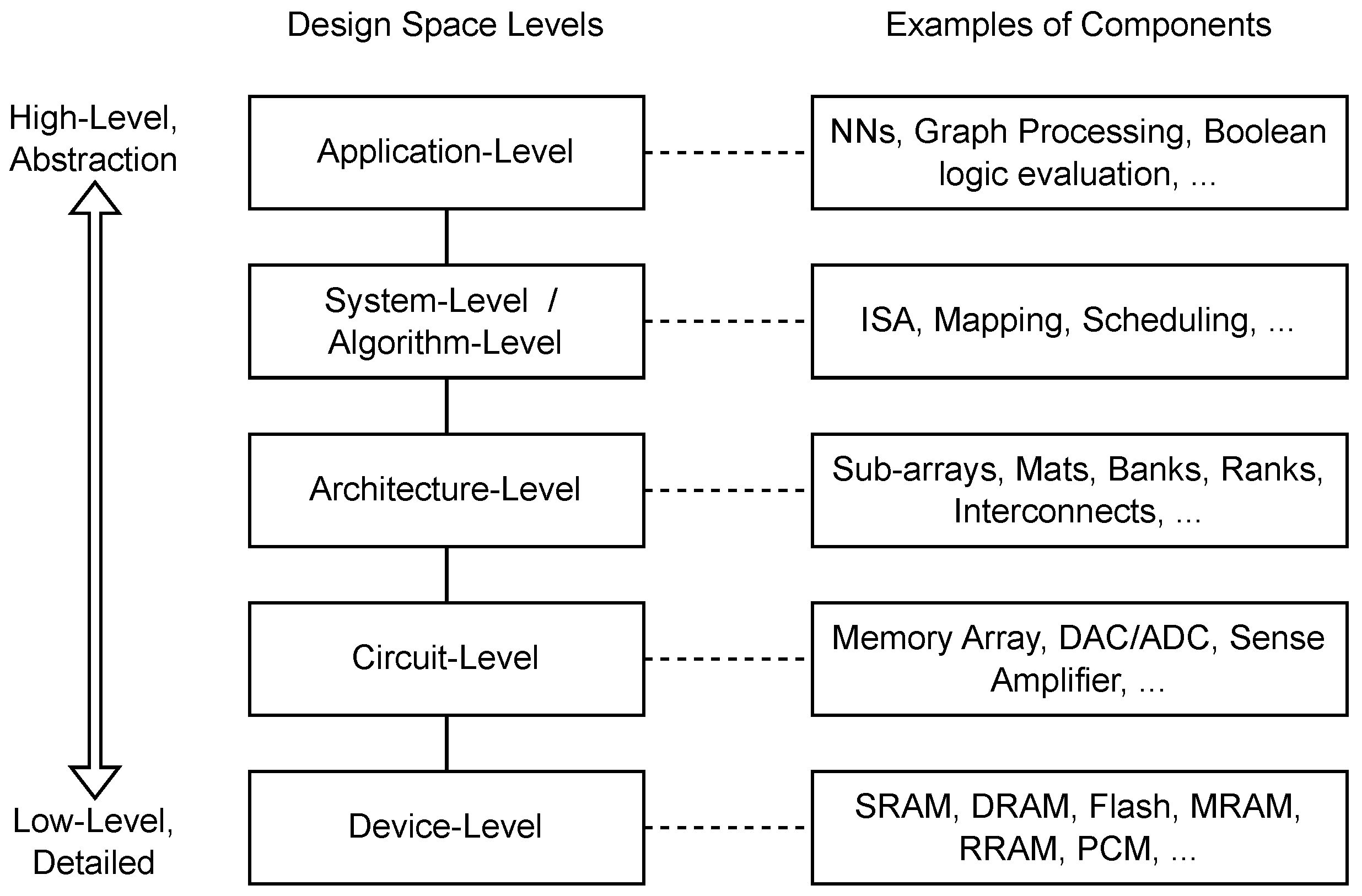

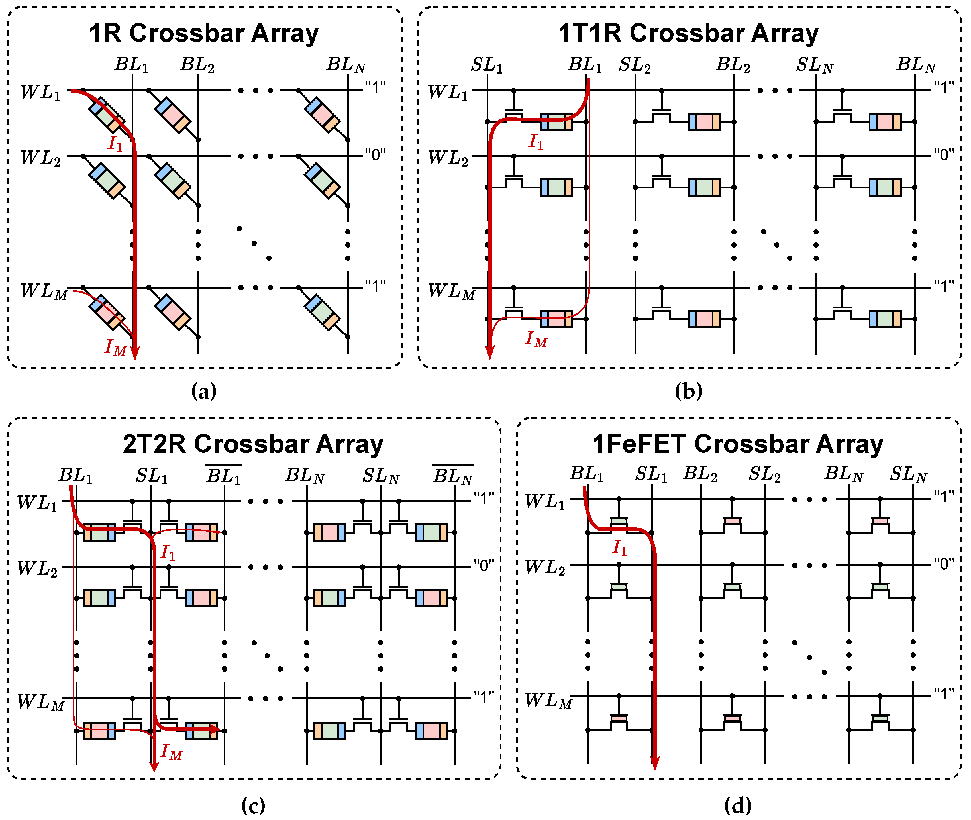

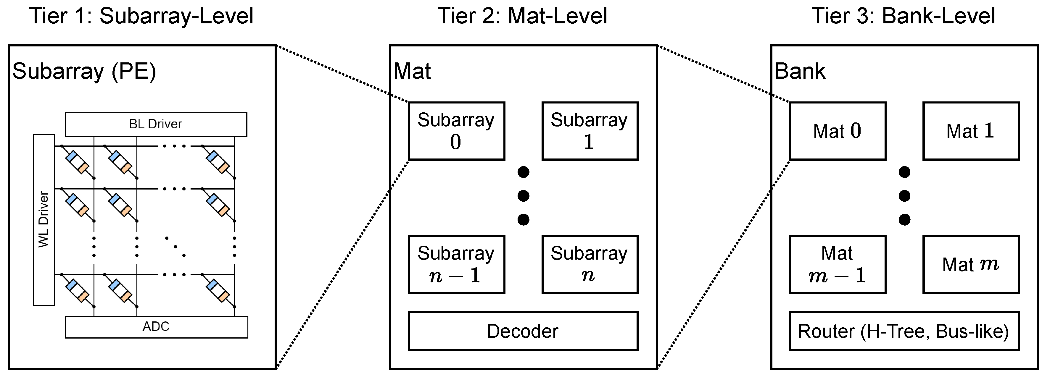

Disclaimer/Publisher’s Note: The statements, opinions and data contained in all publications are solely those of the individual author(s) and contributor(s) and not of MDPI and/or the editor(s). MDPI and/or the editor(s) disclaim responsibility for any injury to people or property resulting from any ideas, methods, instructions or products referred to in the content. |
© 2025 by the authors. Licensee MDPI, Basel, Switzerland. This article is an open access article distributed under the terms and conditions of the Creative Commons Attribution (CC BY) license (https://creativecommons.org/licenses/by/4.0/).